Note : Les descriptions sont présentées dans la langue officielle dans laquelle elles ont été soumises.
I
CA 02828227 2013-09-26
74769-703E
1
DELAY LOCK LOOPS FOR WIRELESS COMMUNICATION SYSTEMS
Divisional Application
This application is a divisional of Canadian Patent Application No. 2,776,873
filed
May 10, 2012 which is a divisional of National Phase Parent Application No.
2,435,440 filed
January 17, 2002.
BACKGROUND
Field
[1001] The present invention relates generally to data communication,
and more
specifically to delay lock loops (DLL) for use in wireless communication
systems.
Background
[1002] In a wireless communication system, an RF modulated signal
from a transmitter
may reach a receiver via a number of propagation paths (e.g., a line-of-sight
path and/or reflected
paths). The characteristics of the propagation paths typically vary over time
due to a number of
factors such as fading and multipath. To provide diversity against deleterious
path effects and
improve performance, multiple antennas may be used to receive the transmitted
signal. If the
propagation paths between the transmit antenna and the multiple receive
antennas are linearly
independent to at least an extent, then the likelihood of correctly receiving
a data transmission
increases with the use of additional receive antennas.
[1003] In a multipath environment, the signal received on each
antenna may include a
number of instances of the transmitted signal. If multiple receive antennas
are used to provide
receive diversity, then each propagation path results in a signal instance
appearing at each of the
multiple receive antennas. If these antennas are located within close
proximity to one another,
then the multiple signal instances received on these antennas for any given
propagation path will
be closely aligned in time but may have different (and possibly wide ranging)
amplitudes and
phases depending on the specific channel gains for the receive antennas.
[1004] At the receiver, each received signal is conditioned and
digitized to provide a
respective stream of data samples. A rake receiver may then be used to process
one or
CA 02828227 2013-09-26
WO 02/071647 PCT/US02/01793
2
more signal instances in each received signal. Improved performance may be
achieved
if the various signal instances in the multiple received signals can be
processed and
combined in a manner such that more of the signal energy is collected for a
given data
transmission.
=
[1005] One key challenge to achieving high performance is to
properly sample each
signal instance at the specific time instances associated with the highest
signal-to-noise-
and-interference ratio (SINR). If receive diversity is not used (i.e., only
one receive
antenna is employed), then a delay lock loop may be used to adjust the sample
timing
for each signal instance such that the received signal is effectively sampled
(or
resampled) at or near the optimum time instances. However, when receive
diversity is
used, certain challenges are encountered in deriving the proper sample timing
for the
multiple signal instances received on multiple antennas for each propagation
path.
[1006] Moreover, additional challenges are encountered in
deriving the proper
sample timing for certain operating conditions. For a communication system
designed
to operate at low SINRs, such as an IS-95 CDMA system, the SINR of a signal
instance
is not quite as sensitive to errors or jitter in the sample timing. However,
for a system
designed to operate at high SINRs, such as an IS-856 CDMA system, errors or
jitter in
the sample timing may result in more noticeable degradation in the signal
instance's
SINR, which may then degrade performance.
[1007] There is therefore a need in the art for techniques to
provide proper sample
timing for receive diversity and/or high SINR operating environments.
SUMMARY
[1008] Techniques are provided herein to derive the sample
timing to be used for
multiple signal instances received on multiple antennas for a given
propagation path
when receive diversity is employed at the receiver. In one receive diversity
delay lock
loop (DLL) scheme, a DLL is maintained for each propagation path, and each DLL
tracks the timing of the best signal instance for the assigned propagation
path. The best
signal instance may be the one achieving the highest signal-to-noise-and-
interference
ratio (SINR) among the multiple signal instances received for the propagation
path. In
another receive diversity DLL scheme, a DLL is maintained for each propagation
path,
and each DLL tracks the average timing of multiple signal instances for the
assigned
propagation path. The average timing for a given propagation path may be
derived by
(1) deriving an error metric indicative of the error in the sampling timing
for each signal
CA 02828227 2013-09-26 =
74769-703E
=
3
instance, (2) weighting the error metrics for the multiple signal instances,
(3) combining
the weighted error metrics for each loop update period to derive a composite
error
metric, and (4) updating a loop filter for the DLL with the composite error
metric. For
both DLL schemes, the sample timing for the multiple signal instances for each
propagation path is derived by the DLL maintained for the propagation path.
These and
other DLL schemes are described in further detail below.
[1009] Techniques are also provided herein to provide sample timing
having
reduced jitter for high SINR operating environments. The SINR of a received
signal
instance may be estimated for a number of different time offsets, with each
time offset
corresponding to a different sample timing for the signal instance. The loop
filter for
= the DLL maintained for the signal instance May initially be updated in
the normal
manner based on an error metric derived for the signal instance. If a change
(e.g., of
one or more chipx8 time units) in the time Offset to be used for the sample
timing is
= detected, then the SINE. for the new time offset is compared to the SINR
for the prior
time offset. The new time offset is. then used for the sample timing if the
SINR for the
new time offset is better (e.g., by y dB) than the SINR = for the prior time
offset.
= Otherwise, if the SINR for the new time offset is not better, then the
prior time offset is
=
retained and used for the sample timing. Again, various details of these
techniques are =
= described below.
[1010] Various aspects and embodiments of the invention are
described in further
detail below. The invention further provides methods, program codes, digital
signal
=
processors (DSPs), receiver units, terminals, base stations, systems, and
other
apparatuses and elements that implement various aspects, embodiments, and
features of
the invention, as described in further detail below.
=
=
=
=
CA 02828227 2013-09-26
74769-703E
3a
According to one aspect of the present ,invention, there is provided a method
for deriving sample timing for a received signal instance at a receiver unit
in a wireless
communication system, comprising: estimating a signal quality of the signal
instance;
determining a current operating mode for a delay lock loop used to provide the
sample timing
for the signal instance, wherein the delay lock loop is operable in one of a
plurality of
operating modes at any given moment; and switching to a new operating mode for
the delay
lock loop if the estimated signal quality surpasses a threshold associated
with the new
operating mode.
According to another aspect of the present invention, there is provided a
digital
processor comprising: at least one pilot processor operative to estimate a
signal quality of a
received signal instance and to derive an error metric indicative of an error
in the sample
timing for the signal instance; a loop filter operative to accumulate the
error metric derived for
the signal instance; and a control unit operative to determine a current
operating mode for a
delay lock loop implemented in part by the loop filter and used to provide the
sample timing
for the signal instance, wherein the delay lock loop is operable in one of a
plurality of
operating modes at any given moment, and wherein the control unit is further
operative to
switch to a new operating mode for the delay lock loop if the estimated signal
quality
surpasses a threshold associated with the new operating mode.
BRIEF DESCRIPTION OF THE DRAWINGS
[1011] The features, nature, and advantages of the present invention will
become more
apparent from the detailed description set forth below when taken in
conjunction with the
drawings in which like reference characters identify correspondingly
throughout and wherein:
[1012] FIG. 1 is a block diagram of an embodiment of a receiver unit
capable of
implementing various aspects and embodiments of the invention;
[1013] FIG. 2 is a diagram of a transmission (or slot) format defined by IS-
856 for the
forward link;
CA 02828227 2013-09-26
WO 02/071647 PCT/US02/01793
4
[1014] FIG. 3
graphically illustrates .an emb9diment of the resampling performed on
the data samples to achieve higher time resolution;
[1015] FIG.
4A is a block diagram of an embodiment of a DSP that includes a
number of pilot processors, each with a loop filter for tracking the timing of
the signal
instance assigned to the pilot processor;
[1016] FIG.
4B is a block diagram of an embodiment of a DSP that includes a
number of pilot processors and a single loop filter for tracking the timing of
all signal
instances of a given propagation path;
[1017] FIG.
4C is a block diagram of an embodiment of a DSP that includes a
master pilot processor and two slave pilot processors used to reduce sample
timing
jitter;
[1018] FIGS.
5A and 5B are block diagrams of an embodiment of a first-order loop
= filter and a second-order loop filter, respectively, for a delay lock
loop;
[1019] FIGS.
5C and 5D are block diagrams of two embodiments of a first-order
loop filter that may be used to track the average timing of multiple signal
instances for a
given propagation path;
[1020] FIGS.
6A and 6B are flow diagrams of two embodiments of a process for
deriving sample timing for a given propagation path based on the timing of the
best
signal instance;
[1021] FIG.
6C is flow diagram of an embodiment of a process for deriving sample
timing for a given propagation path based on the average timing of the signal
instances;
and
[1022] FIG.
6D is a flow diagram of an embodiment of a process for deriving
sample timing with reduced jitter for a received signal instance.
DETAILED DESCRIPTION
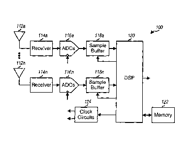
[1023] FIG. 1
is a block diagram of an embodiment of a receiver unit 100 capable of
implementing various aspects and embodiments of the invention. Receiver unit
100
may be implemented within a terminal (e.g., a cellular phone) or a base
station. A
terminal may also be referred to as a mobile station, a remote terminal, an
access
terminal, or some other terminology, and a base station may also be referred
to as an
access point, 'UTRAN, or some other terminology. Receiver unit 100 may also be
used
in various wireless communication systems such as, for example, 1S-95,
cdma2000, IS-
856, and W-CDMA systems. For clarity, various aspects and embodiments are
CA 02828227 2013-09-26
74769-703E
described below for the forward link in an IS-856 system, which is described
in
Document 3GPP2 C.S0024 version 2.0, entitled "cdma2000 High Rate Packet Data
Air Interface Specification", published October 2000.
[1024] In FIG. 1, one or more RF modulated signals transmitted
from one or more
transmitters (e.g., base stations) are received by each of a number of (N)
antennas 112a
through 112n. In general, N can be any integer one or greater (i.e., N 1) and
is equal
to two or more (i.e., N 2) if receive diversity is employed. The received
signal from
each antenna 112 is provided to a respective receiver 114. Each receiver 114
amplifies
a respective received signal with one or more low noise amplifier (LNA)
stages, filters
the amplified RF signal to remove noise and /spurious signals, and quadrature
downconverts the filtered RF signal to provide an inphase (I) and a quadrature
(Q)
. baseband component for the received signal.
[1025] The I and Q baseband components from each receiver 114
are then digitized
by a respective pair of analog-to-digital converters (ADCs) 116 to provide a
stream of
(complex) I and Q samples. In a specific embodiment, .ADCs 116. provide I and
Q
samples at twice the chip rate (i.e., chipx2), with the chip rate being 1.2288
Mcps for
some CDMA systems. The pair of I and Q samples for each chipx2 sample period
is
referred to herein as an ADC sample or a data sample. The stream of ADC
samples
from each pair of ADCs 116 is provided to a respective sample buffer 118 and
stored.
[1026] = A digital signal processor (DSP) 120 receives the ADC samples stored
in
sample buffers 118a through 1.18n and further processes the samples. DSP 120
may
= perform a number of functions such as filtering, resampling,
demodulation, decoding,
and so on. DSP 120 may also implement various control loops used to provide
the
proper sample timing for each received signal, as described in further detail
below. A
memory 122 may be used to provide storage for data and/or codes used by DSP
120.
[1027] Clock circuits 124 provide the clock signals used by
various elements of
= receiver unit 100. For example, clock circuits 124 may be designed to
provide the local
oscillator (LO) signals for receivers 114a through 114n, and the sampling
clocks for
ADCs 116a through 116n. The frequency and/or phase of these various clock
signals
may be adjusted by one or more loop controls from DSP 120.
[1928] FIG. 2 is a diagram of a transmission (or slot) format
defined by IS-856 for
the forward link. Each active slot is divided into two half-slots, with each
half-slot
including two data partitions 212 separated by a pilot burst 214. Data
partitions 212
may be used to transmit user-specific data and signaling, and pilot bursts 214
may be
CA 02828227 2013-09-26
=
=
WO 02/071647 PCT/US02/01793
6
used to transmit a pilot. The left hag-slot includes data partitions 212a and
212b
separated by pilot burst 214a, and the right half-slot includes data
partitions 212c and
212d separated by pilot burst 214b. For IS-856, each pilot burst 214 comprises
96 chips
of all-zero data.
[1029] The left half-slot further includes two signaling bursts
216a and 216b placed
on both sides of pilot burst 214a, and the right half-slot further includes
signaling bursts
216c and 216d placed on both sides of pilot burst 214b. These signaling bursts
216 are
used to implement a MAC channel that is used to transmit reverse power control
(RPC)
information and other information. The RPC information directs the terminals
to adjust
their transmit power either up or down to achieve the desired signal quality
at the
receiving base station.
[1030] Each idle slot is also divided into two half-slots, and
each half-slot also
. includes one pilot burst 214 of the same width (e.g., 96 chips)
and located in the same
position in the half-slot as in the active slot. Two signaling bursts 216
(each of 64 chips
= in duration) are positioned on both sides of each pilot burst 214. The
signaling bursts
provide a transition period between no transmission and pilot transmission and
between
pilot transmission and no transmission. The transition period allows the pilot
reference
to reach or be near its steady state value for the duration of the (e.g., 96-
chip) pilot
burst. The pilot bursts for the idle slot are intended to be essentially
indistinguishable
from the pilot bursts for the active slot.
[1031] FIG. 3 graphically illustrates an embodiment of the
resampling performed on
the ADC samples to achieve higher time resolution. The received signal from a
particular antenna is typically oversampled at an initial sample rate that is
multiple (e.g.,
2, 4, or 8) times the chip rate to provide higher time resolution. The ADC
samples may
then be decimated down to twice the chip rate (i.e., chipx2) and stored to
sample buffer
118. Storing chipx2 samples instead of higher rate (e.g., chipx8) samples
reduces the
buffer requirement.
[1032] To demodulate a particular signal instance in the
received signal, the ADC
samples are retrieved from the sample buffer and resampled to obtain
interpolated
samples at possibly the same sample rate (e.g., chipx2) but at a specific time
offset
corresponding to the arrival time of the signal instance at the receiver unit.
This time
offset is an approximation of the "optimum" sample timing that provides the
highest
signal-to-noise-and-interference ratio (SINR) for the signal instance. A delay
lock loop
(DLL) may be maintained for each signal instance being processed to provide
the
CA 02828227 2013-09-26
WO 02/071647 PCI7US02/01793
7
proper time offset for that signal instance. ,By using resampling, multiple
signal
instances with different arrival times in the received signal may be processed
by
resampling the same sequence of ADC samples at the specific time offsets
determined
for these signal instances.
[1033] As shown in FIG. 3, the received signal is effectively sampled at
chipx2 and
the ADC samples (which are represented by the solid circles) are stored to the
sample
buffer. For the specific signal instance shown in FIG. 3, the optimum sampling
time
instances occur at to, t1, t2, t3, ta, and so on. The ADC sample timing may
not be locked
to the optimum sample timing for a given signal instance, as shown in FIG. 3.
[1034] In a specific implementation, the resampling is performed at chipx8
time
resolution (i.e., TJ8, where Tc is one chip period). In this case, with linear
interpolation, each pair of chipx2 ADC samples may be resampled at three other
= possible discrete time instances, which are represented by the square
boxes between the
solid circles. The difference between the ADC sampling time instances and the
optimum sampling time instances for the signal instance is denoted as tdjff in
FIG. 3.
However, this value is quantized to chipx8 time resolution and results in a
time offset of
tadj = The resampling is then performed based on the time offset, tadj , to
provide the
interpolated samples for the signal instance, which are represented by the
shaded square
boxes.
[1035] FIG. 4A is a block diagram of an embodiment of a DSP 120a that may
be
used to process the pilots in N received signals from N antennas. As shown in
FIG. 1,
the ADC samples for each received signal are provided to a respective sample
buffer
118 and stored. N sample buffers may thus be used to store the ADC samples for
N
different received signals from N antennas. The ADC samples from each sample
buffer
may thereafter be retrieved and provided to one or more pilot processors 410,
with each
pilot processor being assigned to process a specific signal instance. Each
pilot
processor processes the pilot for its assigned signal instance to recover the
timing and
other information (e.g., the S1NR) for that signal instance, as described
below.
[1036] As noted above, each propagation path results in a signal instance
appearing
in each of the N received signals. For a given propagation path, N pilot
processors 410a
through 410n may thus be assigned to process the N signal instances in N
different
received signals corresponding to the propagation path. For simplicity, FIG.
4A shows
the pilot processors assigned to process the signal instances for one
propagation path.
CA 02828227 2013-09-26
WO 02/071647 PCT/US02/01793
8
[1037] FIG. 4A also shows a specific embodiment of pilot processor 410.
Within
each pilot processor 410, the ADC samples are provided to an interpolator 420
and
resampled (as illustrated in FIG. 3) to provide interpolated samples for the
signal
instance being processed. The resampling is performed based on a timing
control
provided by a timing generator 432. This timing control indicates the specific
time
offset, tadi , to be used for resampling the ADC samples, and is provided with
a
particular time resolution (e.g., chipx8 or TA resolution). For each chip
period,
interpolator 420 provides an "early" interpolated sample to a despread and
integrate and
dump (I & D) element 422a, a "late" interpolated sample to a despread I & D
element
422b, and an "on-time" interpolated sample to a despread I & D element 422c.
The
early, late, and on-time samples have the timing relationship shown in FIG. 3
and are
separated by Tc/2, although some other time differences beside Tc/2 may also
be used -
and are within the scope of the invention.
[10381 A PN generator 434 also provides to each despread I & D element 422
a PN
sequence having a specific PN state (or PN phase) corresponding to the arrival
time of
the signal instance being processed. This PN state may be determined by a
searcher in
its search for strong signal instances in the received signal and is provided
to PN
generator 434. Each despread I & D element 422 then despreads its received
interpolated samples with the PN sequence to provide despread samples, and
further
decovers the despread samples with the channelization code used for the pilot.
For
many CDMA systems, the channelization code for the pilot is a sequence of
zeros (e.g.,
Walsh code zero), in which case the decovering may be omitted. For the pilot
structure
shown in FIG. 2, each despread I & D element 422 further accumulates (i.e.,
integrates)
the despread samples over a 96-chip period for each pilot burst to provide a
pilot sample
for the pilot burst (i.e., one pilot sample for each half-slot).
[1039] The pilot samples from despread I & D elements 422a and 422b are
provided
to magnitude squarers 424a and 424b, respectively. Each magnitude squarer 424
computes the energy of each pilot sample (which is a complex value denoted as
+ jPQ ), as follows:
E p = PQ2 . Eq (1)
CA 02828227 2013-09-26
WO 02/071647 PCT/US02/01793
9
Magnitude squarer 424a provides the pilot energy, Ep, early derived based on
the early
samples, and magnitude squarer 424b provides the pilot energy, Ep,late derived
based
on the late samples. For each half-slot, a summer 426 subtracts the late pilot
sample
energy, Epoate , from the early pilot sample energy, Ep,eady, and provides the
difference
(i.e., EP, ly ¨ EP, late ) to a loop filter 430.
[1040] Despread I & D elements 422a and 422b, magnitude squarers 424a and
424b, and summer 426 collectively form an early/late discriminator (or
early/late
detector) that is commonly used to estimate the instantaneous error in the
sample
timing. Other types of discriminator may also be used for a delay lock loop,
and this is
within the scope of the invention.
[1041] Loop filter 430 is part of a delay lock loop (DLL) implemented for
the signal
instance being processed. The output from summer 426 is an error metric, EM,
derived
based on early/late pilot energies and is indicative of the instantaneous
error, At, in the
sample timing for the signal instance. This error metric is filtered by loop
filter 430 to
provide a loop output indicative of the (fine-grain) error, tdiff , between
the ADC
. sampling time instances and the optimum sampling time instances for this
signal
instance. Timing generator 432 then receives and quantizes the loop output to
provide
the (coarse-grain) time offset, tadi , to be used for resampling the ADC
samples. Timing
generator 432 then provides to interpolator 420 the timing control indicative
of the time
offset, tadi , and further provides to sample buffer 118 an address indicative
of the
specific ADC samples to be retrieved from the sample buffer.
[1042] The on-time pilot samples from despread I & D element 422c are
provided
to a pilot filter 436 and filtered based on a particular lowpass filter
response to provide a
filtered pilot. The filtered pilot is then provided to a controller 440 and
may further be
processed to provide an estimate of the pilot S1NR. In much of the following
description, the pilot S1NR is used as an estimate of the signal quality of
the signal
instance. However, other metrics may also be used to estimate the signal
quality of the
signal instance, and this is within the scope of the invention. Despread I & D
element
422c and pilot filter 436 are parts of a signal quality estimator used to
estimate the 51NR
of a signal instance.
[1043] FIG. 4B is a block diagram of an embodiment of a DSP 120b wherein a
single loop filter is provided for the delay lock loop for all N signal
instances of a given
CA 02828227 2013-09-26
WO 02/071647 PCT/US02/01793
propagation path. Similar to the embodiment shown in FIG. 4A, one pilot
processor
411 may be used to process each signal instance received for the propagation
path, and
N pilot processors may thus be used for N signal instances received on N
antennas for
the propagation path. However, each pilot processor 411 does not include a
loop filter
or a timing generator to individually track the timing of its assigned signal
instance.
Instead, one loop filter 430 and one timing generator 432 are used to track
(1) the timing
of the best signal instance, (2) the average timing of all N signal instances,
(3) the
average timing of a subset of the N signal instances, or (4) some other
timing. Timing
generator 432 then provides the timing controls for interpolators 420 for all
N pilot
processors 411 and the addresses for all N sample buffers 118.
[1044] FIG. 5A is a block diagram of an embodiment of a first-order loop
filter
430a for a delay lock loop. Loop filter 430a may be used for loop filter 430
in FIG. 4A,
and includes a single accumulator implemented with a register 512 and a summer
514.
The loop filter input (which is the error metric, EM, from summer 426) is
initially
scaled with a scaling factor, cl, by a multiplier 516, and the scaled value is
then
accumulated by the accumulator. The output from the accumulator comprises the
loop
output, LFout, which is provided to timing generator 432a. The loop output is
indicative of the fine-grain timing difference, tdiff, , between the ADC and
optimum
sampling time instances, and may have any number of bits of resolution. In an
embodiment, the loop output is quantized to chipx8 time resolution by a
quantizer 532
within timing generator 432a to provide the timing control (which is
indicative of the
coarse-grain time offset, tadj ) for interpolator 420.
[1045] FIG. 5B is a block diagram of an embodiment of a second-order loop
filter
430b for a delay lock loop. Loop filter 430b may also be used for loop filter
430 in
FIG. 4A, but includes two accumulators. The first accumulator is implemented
with a
register 512a and a summer 514a, and the second accumulator is implemented
with a
register 512b and a summer 514b. The loop filter input is scaled with a
scaling factor,
ci, by a multiplier 516a, and also scaled with a scaling factor, co, by a
multiplier 516b.
The scaled value from multiplier 516a is accumulated by the first accumulator.
The
output from the first accumulator and the scaled value from multiplier 516b
are summed
by a summer 518, and the summed value is further accumulated by the second
accumulator. The output from the second accumulator comprises the loop output,
t
CA 02828227 2013-09-26
74769-703E
11.
LFout, which is provided to timing generator 432b. The first and second
accumulators
may each have any number of bits of resolution.
[1046] In general, each loop filter may be viewed as comprising a
"loop
accumulator" for accumulating the instantaneous timing errors estimated by the
error
metric, EM. For the first-order loop filter 430a, the loop accumulator
comprises a
single accumulator. And for the second-order loop filter 4301), the loop
accumulator
comprises the first and second accumulators.
[1047] The performance of a delay lock loop with an early-late
discriminator (such
as that shown in FIG. 4A) and with a first or second-order loop filter is
described in
various references available in the art. One such reference is a book by Ai
Viterbi,
entitled "Principles of Spread Spectrum Multiple Access Communications," rd
McGraw Hill, 1977.
=
Diversity DLL
[1048] As noted above, when receive diversity is employed, N signal
instances are
received on N antennas for each propagation path. If the receive antennas are
located in
close proximity to one another, then these signal instances will be closely
aped in
time. However, for a given propagation path, each receive antenna may be
associated
with different fading and multipath effects. Thus, these N signal instances
may be
associated with different (possibly wide ranging) amplitudes and phases.
[1049] Various schemes are provided herein to derive the "proper"
sample timing
for each propagation path when receive diversity is employed. Some of these
schemes
are described below.
[1050] In a first diversity DLL scheme, a DLL is maintained for
each propagation
path, and each DLL is operated to track the timing of the "best" signal
instance for the
assigned propagation path. For each propagation path, the sample timing for
the
remaining signal instances are "slaved" to the sample timing of the best
signal instance.
= The best signal instance may be defined as the one with the best signal
quality (i.e., the
highest SINIR) or the strongest signal strength. The SINR of a particular
signal instance
may be estimated based on the SINR of the pilot, which may in turn. be
estimated based
on the pilot samples from despread I & D element 422c or the filtered pilot
from pilot
filter 436.
[1051] The first DLL scheme may be implemented using the pilot
processor design
shown in FIG. 4A whereby one loop filter 430 is included in each pilot
processor 410.
CA 02828227 2013-09-26
WO 02/071647 PCT/US02/01793
12
Each loop filter is initially updated based on the error metric, EM, derived
for the
assigned signal instance. The loop filter value for the best signal instance
is then
provided to the loop filters for the other signal instances, as described in
further detail
below.
[1052] FIG. 6A is a flow diagram of an embodiment of a process 600 for
deriving
the sample timing for a given propagation path based on the timing of the best
signal
instance. For this embodiment, one loop filter is assigned to each of the N
signal
instances for the propagation path being processed (step 612). Each loop
filter is
initially operated as if receive diversity is not employed, and thus updates
its loop
accumulator based on the error metric, EM, derived from the early/late pilot
energies for
the assigned signal instance, as described above for FIG. 4A (step 614). The
SINR of
each signal instance is also estimated (e.g., based on the pilot samples or
the filtered
pilot) (step 616).
[1053] After the N loop filters have been updated based on their respective
error
metrics derived from their respective sequences of ADC samples, the SINRs of
all N
signal instances are compared (e.g., by controller 440) (step 618). The signal
instance
with the best SINR is then identified as the best signal instance, and the
loop filter value
for this signal instance is then retrieved (step 620). The loop filter value
is denoted as
Lfout in FIG. 4A and comprises the value(s) for register(s) 512 used to
implement the
loop accumulator. The loop filter value for the best signal instance (denoted
as LFoutx
in FIG. 4A) is then provided to the loop filters for the other (N-1) signal
instances and
loaded onto register(s) 512 of these loop filters (step 622). The process may
be repeated
each time a new error metric is derived, which may be every half-slot for the
pilot
structure shown in FIG. 2.
[1054] The first DLL scheme may also be implemented using the pilot
processor
design shown in FIG. 4B whereby one loop filter 430 is provided for N pilot
processors
411. The loop filter is then updated based on the error metric, EM, derived
for the best
signal instance.
[1055] FIG. 5C is a block diagram of an embodiment of a first-order loop
filter
430x that may be used to track the timing of the best signal instance for a
given
multipath. Loop filter 430x may be used for loop filter 430 in FIG. 4B and
includes a
single accumulator implemented with register 512 and summer 514. The error
metrics,
EM1 through EMn, from N pilot processors 411 assigned to the N signal
instances for
the propagation path are provided to a multiplexer 520. Each error metric,
EMi, is
I
CA 02828227 2013-09-26
WO 02/071647 PCMS02/01793
13
derived by a respective pilot processor 411 based on a respective sequence of
ADC
samples for the assigned signal instance. Multiplexer 520 also receives a
control signal,
Select, indicative of the best signal instance, selects the error metric, EMx,
for the best
signal instance, and provides the selected error metric, EMx, to multiplier
516. Register
512, summer 514, and multiplier 516 implement the first-order loop filter, as
described
above.
[1056] FIG. 6B is a flow diagram of another embodiment of a process 630 for
deriving the sample timing for a given propagation path based on the timing of
the best
signal instance. For this embodiment, the design shown in FIGS. 4B and SC may
be
used whereby one loop filter is maintained for all N signal instances of the
propagation
= path being processed.
[1057] For each loop update period (e.g., each half-slot), the pilot
processor for each
signal instance derives the error metric, EMI, from the early/late pilot
energies for the
assigned signal instance in the manner described above (step 632). The SINR of
each
signal instance is also estimated (step 634). The SINRs of all N signal
instances are
then compared (e.g., by controller 440) (step 636). The signal instance with
the best
S1NR is then identified as the best signal instance, and the error metric,
EMx, for this
signal instance is selected (step 638). The selected error metric, EMx, for
the best signal
instance is then provided to the loop filter and used to update the loop
accumulator (step
640). The process may be repeated for each loop update period.
[1058] For the first DLL scheme, the timing of the best signal instance is
used for
the remaining signal instances. This scheme may provide improved performance
if
there is a large disparity in the SINRs of the N signal instances for a given
propagation
path, which may be the case in a multipath environment whereby signals may add
constructively at one antenna and destructively at another antenna. As each of
the
signal instances received on the N antennas individually fades in and out, the
timing of
the best signal instance is retained and used for any new signal instance that
becomes
better.
[1059] In a second diversity DLL scheme, one DLL is maintained for each
propagation path, and each DLL is operated to track the average timing of a
set of signal
instances for the assigned propagation path. This set may include all N signal
instances
or a subset of the N signal instances for the assigned propagation path. The
second
DLL scheme may be implemented using DSP 120b shown in FIG. 4B whereby one loop
filter is maintained for all N signal instances of a given propagation path,
with the loop
,
CA 02828227 2013-09-26
WO 02/071647 PCT/US02/01793
14
filter being updated based on the error metrics derived for the selected
signal instances.
The second DLL scheme may provide improved sample timing by using the error
metrics from multiple signal instances instead of just the best signal
instance.
[1060] FIG. 5D is a block diagram of an embodiment of a first-order loop
filter
430y that may be used to track the average timing of a set of selected signal
instances
for a given multipath. Loop filter 430y may be used for loop filter 430 in
FIG. 4B and
includes a single accumulator implemented with register 512 and summer 514.
The
error metrics, EM1 through EMn, from N pilot processors 411 assigned to the N
signal
instances for this propagation path are provided to N multipliers 522a through
522n
within loop filter 430y. Each error metric, EMi, is derived by a respective
pilot
processor 411 based on a respective sequence of ADC samples for the assigned
signal
instance.
[1061] Each multiplier 522 scales the received error metric, EMi, with a
respective
weight, wi, and provides the scaled error metric to a summer 524. Summer 524
then
sums the scaled error metrics for all N signal instances and provides the
composite error
metric, EMt, to multiplier 516. Register 512, summer 514, and multiplier 516
implement the first-order loop filter, as described above.
[1062] Various schemes may be used to weigh the N error metrics for all N
signal
instances to derive the composite error metric, EMt. In a first weighting
scheme, the N
error metrics are weighted by the signal quality of the signal instances
(i.e., w cc SINRi
for the i-th signal instance, where i e {1, ..., N)). The composite error
metric may then
be expressed as:
EMt = Ewi = EMi . Eq (2)
i.1
This weighting scheme results in the delay lock loop tracking more of the
timing of the
better signal instances.
[1063] In a second weighting scheme, the error metrics for the N signal
instances
are linearly combined (i.e., the same weight for all signal instances, or wi
=1.0 ), as
follows:
EMt = EEMi . Eq (3)
r
CA 02828227 2013-09-26
= 74769-703E
The second weighting scheme may provide improved performance in certain
operating
scenarios, such as if the S1NRs of the N signal instances are within a
particular range.
[1064] For all weighting schemes, the signal instances having
poor SINRs may be
totally excluded from the error metric combining. This may be achieved by
comparing the
5 SINR of each signal instance against a threshold SINR, and setting the
weight and/or the error
metric for the signal instance to zero (e.g., w = 0.0) if its SINR is below
the threshold SINR.
[1065] FIG. 6C is a flow diagram of an embodiment of a process
650 for deriving the
sample timing for a given propagation path based on the average timing of the
selected signal
instances. For this embodiment, the design shown in FIGS. 4B and 5C may be
used whereby
10 one loop filter is maintained for all N signal instances of the
propagation path being
processed.
[1066] For each loop update period (e.g., each half-slot), the
pilot processor for each
signal instance derives the error metric, EMi, from the early/late pilot
energies for the
assigned signal instance in the manner described above (step 652). The SINR of
each signal
15 instance is also estimated and may be used to derive a weight for the
signal instance (step
654). The error metrics for the selected signal instances are weighted by
their respective
weights (step 656), and the weighted error metrics are combined to derive the
composite error
metric, EMt, for the current loop update period (step 658). The composite
error metric, EMt,
is then provided to the loop filter and used to update the loop accumulator
(step 660). The
process may be repeated for each loop update period.
[1067] In a third diversity DLL scheme, one DLL is maintained
for each signal
instance being processed, and each DLL is operated to track the individual
timing of the
assigned signal instance. This may be achieved by operating one loop filter
for each signal
instance, with each loop filter being operated independently and updated based
solely on the
error metric derived for its assigned signal instance. This DLL scheme may be
implemented
using the pilot processor design shown in FIG. 4A whereby one loop filter 430
is included in
each pilot processor 410 and is used to track the timing of the assigned
signal instance.
CA 02828227 2013-09-26
= 74769-703E
15a
However, the register(s) within each loop filter are not loaded with the loop
filter value from
another loop filter, as in the case for the first DLL scheme.
[1068] The third scheme may provide improved performance in
certain operating
scenarios, such as if there is a larger difference in the timing of the N
signal instances
,
CA 02828227 2013-09-26
WO 02/071647 PCT/US02/01793
16
for a given propagation path. In this case, tracking the individual timing of
each signal
instance, instead of tracking the timing of the best signal instance or
tracking the
average timing of all N signal instances, may provide improved performance.
[1069] In a fourth diversity DLL scheme, a number of different loop modes
are
supported. Each loop mode may correspond to a respective DLL scheme described
above (e.g., the first and second loop modes may correspond to the first and
second
DLL schemes). The specific loop mode to use for tracking the timing of the N
signal
instances for a given propagation path may be dependent on the SINRs of these
signal
instances. For example, the timing of the best signal instance may be used for
all signal
instances (i.e., the first DLL scheme) if the SINR of the best signal instance
exceeds the
S1NRs of all other signal instances by a particular amount (e.g., 4 d13). And
if the above
condition is not true, then the average timing of all N (or just the selected)
signal
instances for the propagation path may be used if the S11NRs for these signal
instances
fall within a particular window (e.g., 6 dB).
[1070] Other DLL schemes may also be used for receive diversity, and this
is within
the scope of the invention.
DLL for Signals with high SINR
=
[1071] Some communication systems are designed to support high data rates
for
packet data and/or other services. One such communication system is the IS-856
system, which supports data rates ranging from 38.4 Kbps to 2.4576 Mbps on the
forward link. Increasingly higher data rates require correspondingly higher
SINR to
achieve the target packet error rate (PER).
[1072] For a system designed to operate at high SlNRs, such as the IS-856
system,
errors or jitter in the sample timing may result in noticeable degradation in
the signal
SINR, which may then degrade demodulation and decoding performance. The timing
errors or jitter may be exacerbated if the fine-grain timing difference, tdiff
, between the
ADC and optimum sampling time instances, as determined by the loop filter, is
subsequently quantized to a coarse (e.g., chipx8) time resolution to obtain
the time
offset, tadj , used for resampling. In fact, it can be shown that quantization
of the
resample timing is one of the main reasons for DLL jitter, and the resulting
performance
degradation.
i
CA 02828227 2013-09-26
WO 02/071647 PCT/US02/01793
17
[1073] Referring back to FIG. 3, the optimum sampling time instances may
fall
between the possible discrete resample time instances, which may be derived
based on a
chipx8 clock in the example shown in FIG. 3. In this case, the resampling is
performed
at the chipx8 time instances closest to the optimum sampling time instances.
[1074] If the loop filter for a particular delay lock loop is driven solely
by the error
metric from the early/late discriminator, then the loop filter may dither one
or more
chipx8 periods in steady state. When the SINR. of the received signal is high,
the SINR
of the demodulated symbols derived from the interpolated samples (i.e., the
demodulated SINR) is sensitive to jitter in the sample timing caused by the
dithering. In
particular, the jitter in the sample timing leads to an increased variance in
the
demodulated SINR, which then results in a larger difference between the mean
S1NR
and the 2% worst-case SINR. At higher data rates, the degraded demodulated
SINR
may result in a higher packet error rate. The system throughput may then be
degraded
due to (1) retransmission of the error packets, and (2) an increase in the
back-off for the
rate control. Thus, improved performance may be achieved if the sample timing
jitter is
reduced at high signal S1NRs.
[1075] In an embodiment, a delay lock loop may be designed to support
multiple
operating modes, including a normal mode and an enhanced mode. If receive
diversity
is employed, then the enhanced mode may be entered, for example, if the SINR
of any
one of the N signal instances exceeds a particular threshold (e.g., 6 dB). In
the
enhanced mode, various techniques may be used to monitor the jitter of the
loop filter
and to adjust the sample timing only if it would result in better SlNR for the
signal
instance.
[1076] The policy used to determine whether or not the DLL operates in the
enhanced mode can be generalized. For example, the DLL may transition from the
normal mode to the enhanced mode if the SINR exceeds a first threshold, -Lis,
While in
the enhanced mode, the DLL would transition back to the normal mode only if
the
SINR drops below a (usually lower) second threshold, Tfait, (i.e., Zan <
Trise), and would
remain in the enhanced mode otherwise. With this scheme, the transitions
between the
DLL operating modes are governed by SINR hysterisis, which prevents frequent
toggling from one mode to another. Hysterisis may similarly be applied if more
than
two operating modes are used for the DLL.
[10771 FIG. 4C is a block diagram of an embodiment of a DSP 120c that may be
used to reduce sample timing jitter for a received signal with high SINR. DSP
120c
CA 02828227 2013-09-26
74769-703E
18
may be used to implement one embodiment of the enhanced mode for the delay
lock loop. In
this embodiment, two "slave" pilot processors 412a and 412b are assigned to a
signal instance
that achieves high SNR. These slave pilot processors are used in conjunction
with a "master"
pilot processor 413 also assigned to process the signal instance. The master
finger processor
may be implemented with pilot processor 410 or 411, depending on the specific
design of
DSP 120c.
[1078] Slave pilot processors 412a and 412b are used to process the
ADC samples to
determine the pilot SINR at two time offsets that are different from the time
offset associated
with the master pilot processor. In an embodiment, slave pilot processors 412a
and 412b are
assigned offsets of +1 chipx8 period and ¨1 chipx8 period, respectively. Each
slave pilot
processor 412 receives a respective "modified" time offset, tadj,s, for the
signal instance, which
may be obtained by adding or subtracting one chipx8 unit to or from the
"nominal" time
offset, tadj, derived for the signal instance by the master pilot processor.
The modified time
offsets provided to slave pilot processors 412a and 412b may thus be derived
as tadi,si= tadj-1
and tadj,s2= tadj+1, respectively.
[1079] Within each slave pilot processor 412, interpolator 420
resamples the ADC
samples based on the modified time offset, tadis = Despread I & D element 422
then (1)
despreads the interpolated samples with the PN sequence (the same PN sequence
is provided
to the master and slave pilot processors assigned to process a given signal
instance), (2)
accumulates the despread samples over each pilot burst, and (3) provides a
pilot sample for
the pilot burst based on the interpolated samples at the modified time offset.
The pilot
samples from despread I & D element 422 are then filtered by pilot filter 436
to provide a
filtered pilot for the modified time offset. The filtered pilots from slave
pilot processors 412a
and 412b are provided to controller 440 and may further be processed to
provide an estimate
of the pilot SINRs for the modified time offsets of t
-adj,s1 and tadj,s2. Slave pilot processors 412a
and 412b are thus used to determine the pilot SINRs at 1 chipx8 unit from
the time offset,
tadj, determined by the master pilot processor.
CA 02828227 2013-09-26
74769-703E
19
[1080] FIG. 6D is a flow diagram of a specific, embodiment of a
process 670 for
deriving sample timing with reduced jitter for a received signal instance.
Initially, a
determination is made whether or not the pilot SINR for the signal instance is
greater than a
particular threshold (step 672). If the answer is no, then the process returns
to step 672.
Otherwise, if the pilot SINR is greater than the threshold, then the delay
lock loop enters the
enhanced mode and two slave pilot processors are assigned to the signal
instance (step 674).
The modified time offsets for these slave pilot processors are then
determined, and the pilot
SINRs of the slave pilot processors are also initialized (step 676). Because
measurement
noise could cause the pilot SINR of a slave pilot processor to be momentarily
larger than that
of the master pilot processor, which may possibly lead to DLL jitter, the
pilot SINRs of the
slave pilot processors may be set equal to the pilot SINR of the master pilot
processor minus a
particular amount.
[1081] The loop filter of the master pilot processor is updated for
each loop update
period (e.g., every half-slot) based on the error metric derived by the
early/late discriminator
of the master pilot processor (step 682). The output of the loop filter is
monitored for jitter. If
the loop filter output implies retention of the current time offset, tadj,
(step 684), then no
additional processing is required and the process returns to step 682.
Otherwise, if the loop
filter output implies a change in the time offset, tadj, to a new value that
is either +1 or ¨1
chipx8 unit away from the prior value (step 684), then the slave pilot
processor corresponding
to the new time offset is identified (step 686). The pilot SINR of the master
pilot processor is
then compared against the pilot SINR of the identified slave pilot processor,
which was
previously assigned with the new time offset (step 688).
[1082] If the pilot SINR of the identified slave pilot processor is
deemed to be better
than the pilot SINR of the master pilot processor (step 692), then the sample
timing for the
signal instance is allowed to be updated in the normal manner. In an
embodiment, the new
time offset is deemed to be better if the pilot SINR of the identified slave
pilot processor is
greater than the pilot SINR of the master pilot processor by a particular
delta amount (e.g., by
y dB). This delta amount is used to provide hysteresis so that the "better"
time offset is not
continually toggled between two offset values and to provide some level of
immunity to
,
CA 02828227 2013-09-26
74769-703E
19a
measurement noise. New modified time offsets are then determined for the slave
pilot
processors based on the new nominal time offset (step 694). The pilot SINRs of
the slave
pilot processors are also initialized to reflect their assignments with the
new modified time
offsets.
[1083] Otherwise, if the new time offset is deemed to not be better (e.g.,
does not
provide the requisite amount of improvement in the pilot SINR) (step 692),
then the sample
timing for the signal instance is not allowed to be updated. The former loop
CA 02828227 2013-09-26
WO 02/071647 PCT/US02/01793
filter value is retained (e.g., by reversing the prior update to the loop
filter) and the time
offset, tadj , is left unchanged (step 696). The process then returns to step
682 where the
loop filter is updated at the next loop update period.
[1084] In FIG. 6D,
the DLL enters the enhanced mode if the pilot SINR exceeds the
threshold. In another embodiment, the DLL is operated in the enhanced mode
based on
some other criterion (e.g., if higher data rates are used for data
transmission). The DLL
may also be operated in the normal mode during timing acquisition and
thereafter
switched to the enhanced mode during tracking.
[1085] The
enhanced mode described above may be used whether or not receive
diversity is employed. If receive diversity is employed, then the SINR of the
propagation path (i.e., the path SINR) may be used to determine whether or not
to enter
= the enhanced mode. The path S1NR refers to the SINR of the combined
output of all N
pilot processors assigned to the N signal instances for the propagation path.
Alternatively, the SINR of the best signal instance may also be used to
determine
whether or not to enter the enhanced mode.
[1086] In the
above description, a specific design for the DLL is used whereby each
received signal is sampled based on a sampling clock having an arbitrary
timing phase
(i.e., with respect to the optimum sampling time). Resampling is then
performed to
obtain interpolated samples at the "optimum" sampling time instances, which
are
determined by the delay lock loop for the signal instance being processed.
[1087] In another
DLL design, the phase of the sampling clock is adjusted by the
delay lock loop for a selected signal instance in the received signal (e.g.,
the strongest
signal instance). For this DLL design, the selected signal instance would then
be
sampled at or near its optimum sampling time, and resampling would not be
needed for
this signal instance. This DLL design can reduce the amount of jitter in the
sample
timing for the selected signal instance, which may improve the SINR of the
demodulated data. Resampling may be used for the other signal instances in the
received signal.
[1088] Any one of
the diversity DLL schemes described above may also be used in
conjunction with this alternative DLL design. For example, the sampling clocks
for all
N received signals may be adjusted based on the optimum sample timing for the
best
signal instance from among all signal instances in the N received signals
(i.e., the first
diversity DLL scheme). Resampling is then not needed for the N signal
instances
CA 02828227 2013-09-26
WO 02/071647 PCT/US02/01793
21
corresponding to the propagation path with the best signal instance. The
sampling
clocks may also be adjusted based on the average sample timing of the N signal
instances for the propagation path with the best signal instance (i.e., the
second diversity
DLL scheme). The sampling clock for each received signal may also be
individually
adjusted based on the sample timing for the best signal instance on that
received signal
(i.e., the third diversity DLL scheme).
[1089] The delay lock.loops and timing recovery techniques described herein
may
be implemented by various means. For example, a delay lock loop may be
implemented
in hardware, software, or a combination thereof. For a hardware
implementation, the
elements used to implement one or more delay lock loops may be implemented
within
one or more application specific integrated circuits (ASICs), digital signal
processors
(DSPs), digital signal processing devices (DSPDs), programmable logic devices
(PLDs), field programmable gate arrays (FPGAs), processors, controllers, micro-
controllers, microprocessors, other electronic units designed to perform the
functions
described herein, or a combination thereof. A DSP may also be designed with
the
capability to implement multiple pilot processors in parallel or in a time
division-
multiplexed (TDM) manner.
[1090] For a software implementation, all or portions of the delay lock
loops and/or
certain timing recovery techniques may be implemented with modules (e.g.,
procedures,
functions, and so on) that perform the functions described herein. The
software codes
may be stored in a memory unit (e.g., memory 122 in FIG. 1) and executed by a
processor (e.g., DSP 120). The memory unit may be implemented within the
processor
or external to the processor, in which case it can be communicatively coupled
to the
processor via various means as is known in the art.
[1091] The delay lock loops may also be implemented with a combination of
hardware and software. For example, hardware may be used to derive the error
metrics
and generate the timing controls, and software may be used to implement the
loop
filters.
[1092] Headings are included herein for reference and to aid in locating
certain
sections. These headings are not intended to limit the scope of the concepts
described
therein under, and these concepts may have applicability in other sections
throughout
the entire specification.
[1093] The previous description of the disclosed embodiments is provided to
enable
any person skilled in the art to make or use the present invention. Various
I I
CA 02828227 2013-09-26
= 74769-703E
22
modifications to these embodiments will be readily apparent to those skilled
in the art, and the
generic principles defined herein may be applied to other embodiments without
departing
from the scope of the invention. Thus, the present invention is not intended
to be limited to
the embodiments shown herein but is to be accorded the widest scope consistent
with the
principles and novel features disclosed herein.