Note : Les descriptions sont présentées dans la langue officielle dans laquelle elles ont été soumises.
LIGHT EMITTING DEVICE
[0oot] This application claims priority to Japanese Patent Application No.
2012-252211,
filed on November 16, 2012.
BACKGROUND OF THE INVENTION
1. Field of the Invention
[0002] The present invention relates to a light emitting device which includes
a substrate
member and at least one light emitting element.
2. Description of the Related Art
[0003] There has been proposed a light emitting device which includes light
emitting
elements arranged on a flexible substrate member (see JP2005-322937A). The
light emitting
device described in JP2005-322937A can be rolled up during the transportation,
and also can
be cut in a desired size for use.
SUMMARY OF THE INVENTION
[0004] However, in the light emitting device described in JP 2005-322937A,
there is a
problem in that, for example, when the light emitting device is bent,
concentration of stress is
tend to be experienced between the light emitting elements and the substrate
member. The
present invention is devised in the light of such circumstances, and it is
hence an object
thereof to provide a light emitting device in which stress experienced between
a light emitting
element and a substrate member can be reduced.
[00051 A light emitting device according to an aspect of the present invention
includes a
substrate member and at least one light emitting element. The substrate member
includes a
flexible base member, a plurality of wiring portions, and a groove portion.
The flexible base
member has a side extending in a first direction along a longitudinal
direction and a side
extending in a second direction different from the first direction. The wiring
portions are
disposed on the base member. The groove portion is defined between adjacent
ones of the
wiring portions spaced apart from each other. At least one light emitting
element is disposed
on the substrate member and connected to the wiring portions. The groove
portion includes a
first groove portion extending in a direction that forms a slanted angle with
respect to the first
direction, a second groove portion spaced apart from the first groove portion
and extending in
a direction that forms a slanted angle with respect to the first direction,
and a third groove
portion interconnected with the first groove portion and the second groove
portion. The at
least one light emitting element is disposed over the third groove portion.
1
CA 2833466 2018-11-15
CA 02833466 2013-11-15
[0006] According to the present invention, a light emitting device can be
provided
which can prevent stress experienced between at least one light emitting
element and a
substrate member.
BRIEF DESCRIPTION OF DRAWINGS
[0007] FIG. 1 is a plan view of a light emitting device.
[0008] FIG. 2 is an enlarged plan view in the vicinity of a sealing member
shown in
FIG. I.
[0009] FIG. 3 is a cross sectional view taken along line A-A of FIG. 2.
[0010] FIG. 4 is a partially enlarged view of FIG. I.
[0011] FIG. 5 is a plan view of a light emitting device.
[0012] FIG. 6 is an enlarged plan view of a wiring portion.
DETAILED DESCRIPTION OF EMBODIMENTS
[0013] Next, embodiments of the invention will be described with reference to
the
drawings. In the description of the drawings below, the same or similar
components
are denoted by the same or similar reference symbols. However, it should be
noted
that the drawings are drawn schematically, and the dimensional ratios and the
like of the
components may differ from the actual ratios. Accordingly, the specific
dimension
and the like should be determined in consideration of the description below.
In
addition, the drawings may also include the components that have different
dimensional
relations and ratios among one another.
Structure of Light Emitting Device 100
[0014] A structure of a light emitting device 100 according to an embodiment
will be
described with reference to the drawings. FIG. 1 is a plan view showing a
structure of
a light emitting device 100. FIG. 2 shows an enlarged plan view of a sealing
member
20. FIG. 3 is a cross sectional view taken along line A-A of FIG. 2.
[0015] The light emitting device 100 includes a substrate member 10, three
sealing
members 20, and three light emitting elements 30. The light emitting device
100 is
flexible, so that it can be stored rolled-up on a reel etc., and can be
installed along a
curved surface.
1. Structure of Substrate Member 10
[0016] The substrate member 10 is a flexible elongated member. The first
direction
corresponds to the longitudinal direction of the substrate member 10 and the
second
direction which is substantially perpendicular to the first direction
corresponds to the
lateral direction of the substrate member 10. The ratio of the lengths of the
substrate
member 10 in the longitudinal direction and the lateral direction can be
appropriately
selected, and for example, a ratio of 6:1, 30:1, or 100:1 can be employed. The
length
2
CA 02833466 2013-11-15
of the substrate member 10 in the first direction can be, for example, 1150
mm, and the
length of the substrate member 10 in the second direction can be, for example,
15 mm.
The substrate member 10 includes a flexible base member 11, two wiring
portions 12,
two terminal portions 13, three groove portions 14, and a reflection layer 15.
[00171 The base member 11 can be made of a flexible insulating material. For
such
a material, an insulating resin such as polyethylene terephthalate and
polyimide can be
preferably used but is not limited thereto. For example, the base member 11
may be
made of a strip of copper foil or aluminum foil which is covered with an
insulating resin.
The base member 11 can have a thickness of about 10 gm to about 100 gm, for
example.
The material of the base member 11 can be appropriately selected in view of
the type of
mounting of the light emitting elements 30, the reflectance, and adhesion with
other
members, etc. For example, in the case where a solder is used for mounting the
light
emitting elements 30, a polyimide which has a high heat-resisting property is
preferably
used, and in the case where the reflection layer 15 is not disposed on the
base member
11, a material which has a high optical reflectance (for example a white color
material)
is preferably used to obtain a light emitting device having a good light
extraction
efficiency.
10018] In the case where the base member 11 is made solely of a resin, the
resistance
to bending of the substrate member 10 decreases significantly, and thus, the
effects of
the present invention can be exhibited effectively.
[0019] The two wiring portions 12 are arranged on a main surface of the base
member
11. The two wiring portions 12 are arranged between the two terminal
portions 13.
The two wiring portions 12 are placed along the first direction. The two
wiring
portions 12 are arranged spaced apart from each other. With this
configuration, the
groove portion 14 to be described below is defined between the two wiring
portions 12.
The wiring portions 12 as described above are made of a thin metal film such
as a
copper foil or an aluminum foil, for example. The wiring portions 12 have a
thickness
which does not impair the flexibility of the substrate member 10 and a
thickness of 8
iun to 150 pcm is preferable. The wiring portions 12 are preferably arranged
on the
base member 11 respectively with a largest possible area. Widening the surface
area
of the wiring portions 12 allows for increased heat dissipation from the
wiring portions
12. The comers of the wiring portions 12 in a plan view are preferably
rounded for
improving the adhesion (anti-detachment feature) of the wiring portions, which
can
enhance the reliability. The comers are preferably rounded with a radius of
100 gm or
more.
3
CA 02833466 2013-11-15
[0020] The two terminal portions 13 can be arranged on the main surface of the
base
member 11. The two terminal portions 13 can be arranged along the first
direction at
both sides of the two wiring portions 12. Each terminal portion 13 is arranged
spaced
apart from the corresponding wiring portion 12. With this configuration, the
groove
portion 14 is formed in between the terminal portion 13 and the corresponding
wiring
portion 12. An external wiring 13a can be connected to each terminal portion
13.
The external wirings 13a may be connected to corresponding portions of known
connectors disposed on the substrate member 10.
[0021] Three groove portions 14 are formed on the base member 11, as the
groove
portions 14 being defined between the adjacent two wiring portions 12 and
between the
wiring portions 12 and the corresponding terminal portions 13 respectively. As
shown
in FIG. 1, the groove portion 14 as a whole extends generally at a slanted
angle to the
first direction and the second direction. The center portion in the second
direction of
the groove portion 14 is bent in a crank-shape as shown in FIG. 1. The width
of the
groove portion 14 (that is, the interval between the two wiring portions 12,
and the
interval between the wiring portion 12 and the corresponding terminal portion
13) can
be, for example, about 0.05 mm to about 5 mm. The detailed configuration of
the
groove portions 14 will be described below.
[0022] The reflection layer 15 can be used to cover the exposed surfaces of
the base
member 11, two wiring portions 12 and two terminal portions 13. The reflection
layer
15 may also cover the inner surfaces of the groove portions 14. Thus, the
reflection
layer 15 can cover approximately the entire upper surface of the substrate
member 10
except for the openings 15S to be described below. Such a reflection layer 15
is made
of a material which can reflect the emitted light (including the wavelength-
converted
light by a wavelength converting member) from the light emitting elements 30.
For
such a material, an insulating white ink which is a so-called white resist
made of a
silicone resin containing titanium oxide is preferably used but is not limited
thereto.
[0023] Also, the reflection layer 15 is formed with three openings 15S to
dispose
three light emitting elements respectively. FIG. 2 and FIG. 3 show one of the
openings 15S formed over the two wiring portions 12. As shown in FIG. 2 and
FIG. 3,
in the opening 15S, the two wiring portions 12 are exposed. Meanwhile, in the
opening 15S formed over the wiring portion 12 and the terminal portion 13, the
wiring
portion 12 and the terminal portion 13 are exposed.
[0024] The openings 15S can be formed in an appropriate shape such as a
circular
shape or a quadrangular shape adapted to surround the light emitting elements
30 in
plan view, respectively. After the light emitting elements 30 are mounted, the
4
CA 02833466 2013-11-15
openings 15S are preferably covered with an underfill material 106, a sealing
member
20, and/or other appropriate light-reflection member. With this arrangement,
the
portion around the light emitting elements 30 can be protected. At this time,
the use of
a material having a higher optical reflectance than that of the substrate
member 10 and
the wiring portion 12 which are exposed in the opening 15S for the covering
can
improve the light extraction efficiency of the light emitting device.
[0025] Also, the openings 15S can be smaller than the shape in a plan view of
the
light emitting elements 30, with the reflection layer 15 disposed extending
below the
light emitting elements 30. The reflection layer 15 may be disposed to
surround the
bonding member of each light emitting element so that the opening is not
substantially
formed. In this case, the light extraction efficiency can be enhanced without
using an
underfill etc., which is to be described below.
2. Structure of Sealing Member 20
[0026] The three sealing members 20 may be arranged on the substrate member
10.
The three sealing members 20 are disposed so as to enclose the three openings
15S
formed in the reflection layer 15. The three sealing members 20 are placed
along the
first direction. The three sealing members 20 seals the three light emitting
elements 30
respectively. The sealing member 20 is, as shown in FIG. 3, formed in an
approximately hemispherical shape with the light emitting element 30 at the
center, but
is not limited thereto, an appropriate shape such as a rectangular
parallelepiped shape, a
semicircular column shape, etc., can be employed.
[0027] Such sealing members 20 are made up of a light transmissive resin (for
example, an epoxy resin, a urea resin, a silicone resin and the like). The
sealing
members 20 may contain a light diffusing material (barium sulfate, titanium
oxide,
aluminum oxide, silicon oxide, etc.).
[0028] The material of the sealing members 20 is not limited to a resin
material as
described above, and a light-transmissive material such as glass may be
employed.
[0029] The sealing members 20 preferably contains a wavelength converting
member
which can absorb emission from the light emitting elements 30 and emits light
of
different wavelength. With this arrangement, a light emitting device to emit
light of a
desired color can be obtained. Examples of such a wavelength converting member
include an oxide-based fluorescent material, a sulfide-based fluorescent
material, and a
nitride-based fluorescent material. It is preferable that, particularly with
the use of a
gallium nitride based light emitting element to emit blue light as the light
emitting
elements 30, a fluorescent material to absorb blue light, such as a YAG-based
fluorescent material or a LAG-based fluorescent material to emit yellow to
green light, a
CA 02833466 2013-11-15
SiAlON-based fluorescent material to emit green light, and a SCASN-based
fluorescent
material and a CASN-based fluorescent material to emit red light, are
preferably used
singly or in combination. With this arrangement, a light emitting device to
emit white
light can be obtained.
[0030] More specifically, for the light emitting devices used for the display
devices
such as backlights of liquid crystal displays and TV-screens, a SiAlON-based
fluorescent material and a SCASN-based fluorescent material are preferably
used singly
or in combination. With this arrangement, a light emitting device having high
color
reproducibility can be obtained. Also, in a light emitting device for lighting
applications, a YAG-based fluorescent material or a LAG-based fluorescent
material
and a SCASN-based fluorescent material or a CASN-based fluorescent material
are
preferably used in combination. With this arrangement, a lighting device
having high
color rendering property can be obtained.
[0031] The use of the wavelength converting member as described above is not
limited to be contained in the sealing member 20, but can be used external of
the light
emitting device 100, for example, disposed in a display device or a lighting
device
which uses the light emitting device 100 as its light source.
3. Structure of Light Emitting Element
[0032] The three light emitting elements 30 are arranged on the substrate
member 10.
The three light emitting elements 30 can be respectively disposed in the three
openings
15S formed in the reflection layer 15. The three light emitting elements 30
are placed
along the first direction. The light emitting element 30 placed at the middle
of the
three light emitting elements 30 is connected to two wiring portions 12. The
light
emitting elements 30 at each side of the three light emitting elements 30 are
connected
to the wiring portion 12 and the terminal portion 13 respectively. As shown in
FIG. 2,
each light emitting element 30 is arranged along the second direction and the
longitudinal direction of each light emitting element 30 can be in parallel
with the
second direction.
[0033] In the embodiment, each of the three light emitting elements 30 is, as
shown in
FIG. 3, mounted on the substrate member 10 in a flip-chip manner. Each light
emitting element 30 is connected to a pair of wiring portions 12 via a pair of
bonding
members 105 respectively. The bonding member 105 can be made of, for example,
a
solder such as a Sn-Ag-Cu based solder, an Au-Sn base solder, or a Sn-Cu based
solder,
a metal such as Au, an anisotropic conductive paste, or an Ag paste. An
underfill
material 106 can be filled between each light emitting element 30 and the base
member
11. The
underfill material 106 is, as shown in FIG. 2, preferably disposed not only on
6
CA 02833466 2013-11-15
the two wiring portions 12 but also on the reflection layer 15. With this
arrangement,
the light extraction efficiency can be enhanced and also the light emitting
elements 30
can be supported firmly. The underfill material 106 can be made of, for
example, a
silicone resin or an epoxy resin, a fluororesin, or a hybrid resin containing
one or more
those resins. The underfill material 106 preferably has a light reflecting
property by
containing titanium oxide, silicon oxide, or alumina, which has a white color.
With
this arrangement, the light extraction efficiency of the light emitting
elements can be
enhanced.
[0034] Also, as shown in FIG. 3, the light emitting element 30 may include a
semiconductor structure 31, a p-side electrode 32, an n-side electrode 33, and
an
insulating layer 34. The semiconductor structure 31 includes an n-type layer,
an active
layer, and a p-type layer which are stacked in the order on a light-
transmissive sapphire
substrate. The n-type layer, the active layer and the p-type layers can be
respectively
made of, for example, a gallium nitride-based semiconductor. The p-side
electrode 32
and the n-side electrode 33 are respectively connected to a pair of wiring
portions 12 via
a pair of bonding members 105. The n-side electrode 33 can extend to a lower
portion
of the p-type layer via the insulating material layer 34. The p-side electrode
32 and the
n-side electrode 33 are disposed so that the portions facing each other can be
in parallel
with each other. This arrangement facilitates disposition (mounting) over the
third
groove portion 143 (see FIG. 4) to be described below. The p-side electrode 32
and
the n-side electrode 33 preferably have approximately same size and shape.
With this
arrangement, the stress experienced on the light emitting elements 30 caused
by bending
of the substrate member 10 can be dispersed, so that malfunction of the light
emitting
elements 30 can be reduced.
Configuration of Groove Portion 14
[0035] Next, the configuration of the groove portion 14 will be described with
reference to the drawings. FIG. 4 shows a partially enlarged view of FIG. 1.
The
groove portion 14 includes a first groove portion 141, a second groove portion
142, and
a third groove portion 143.
[0036] The first groove portion 141 extends along the direction (hereinafter
referred
to as a "third direction") which is at an angle al (0 <al <90 ) to the first
direction.
The second groove portion 142 extends along the direction which is at an angle
a2 (0
<a2 <90 ) to the first direction. The first groove portion 141 and the second
groove
portion 142 are spaced apart from each other in the first direction. Also, the
first
groove portion 141 and the second groove portion 142 are spaced apart from
each other
in the second direction. Thus, the first groove portions 141 and the second
groove
CA 02833466 2013-11-15
portions 142 are not formed on the same straight line. In the present
embodiment, the
first groove portion 141 and the second groove portion 142 may have similar
lengths to
each other, but according to the location of the light emitting element 30,
different
length may be employed. In the present embodiment, the first groove portion
141 and
the second groove portion 142 are substantially in parallel with each other
(o4=a2=a)
but they may be formed so as not to be parallel to each other (a4a2).
[0037] A third groove portion 143 is interconnected with a first groove
portion 141
and a second groove portion 142. The third groove portion 143 extends along
the first
direction. Thus, the third groove portion 143 is, as shown in FIG. 4, at an
angle
greater than 90 degrees to the first groove portion 141 and the second groove
portion
142, respectively. In the present embodiment, the third groove portion 143 has
a
length smaller than the respective lengths of the first groove portion 141 and
the second
groove portion 142, but the length is not limited to them.
[0038] In this embodiment, the light emitting element 30 is disposed over the
third
groove portion 143. The light emitting element 30 is spaced apart from the
first
groove portion 141. The light emitting element 30 is spaced apart from the
second
groove portion 142. Thus, the light emitting element 30 is disposed only over
the third
groove portion 143 of the groove portion 14. In a similar manner, a sealing
member
20 which seals the light emitting element 30 is arranged over the third groove
portions
143. The sealing member 20 is spaced apart from the first groove portion 141.
The
sealing member 20 is spaced apart from the second groove portion 142. Thus,
the
sealing member 20 is disposed only over the third groove portion 143 of the
groove
portion 14. The sealing member 20 is preferably spaced apart from the first
groove
portion 141 and the second groove portion 142 respectively at 0.5 mm or
greater, in the
first direction.
[0039] The angle al of the first groove portion 141 to the first direction is
preferably
30 degrees or greater. With the angle al of 30 degrees or greater, the
reflection layer
15 can be prevented from being damaged by the comer of the wiring portion 12.
Particularly, with the angle al of 45 degrees or greater, the reflection layer
15 can be
further prevented from being damaged by the corner of the wiring portion 12
when the
substrate member 10 bends. Also, with the angle al in a range of 70 degrees to
85
degrees, the arrangement degree of freedom of the sealing member 20 and the
light
emitting element 30 can be improved. The above can be applied in a similar
manner to
the angle at of the second groove portion 142 to the first direction.
8
CA 02833466 2013-11-15
[0040] The light emitting device 100 as described above employs the flexible
substrate member 10, so that a roll-to-roll processing method can be used for
manufacturing.
Performance and Effects
[0041] In the light emitting device 100, the groove portion 14 includes a
first groove
portion 141 and the second groove portion 142 each extending in the third
direction and
a third groove portion 143 interconnected with the first groove portion 141
and the
second groove portion 142. Each light emitting element 30 is disposed over the
third
groove portion 143.
[0042] The light emitting device 100 has a smaller thickness at the groove
portion 14.
Therefore, if the groove portions 14 are formed along the second direction, at
the time
when the light emitting device 100 is rolled up in the first direction, the
light emitting
device 100 bends at a small curvature at the groove portions 14. As a result,
a large
stress may be experienced between the light emitting element 30 and the
substrate
member 10.
[0043] Whereas, in the present embodiment, the first groove portion 141 and
the
second groove portion 142 extend in the third direction which is different
from the
second direction. As a result, even in the case where the light emitting
device 100 is
rolled up in the first direction, the light emitting device 100 can be
prevented from
bending with a small curvature at the groove portion 14. Thus, a large stress
can be
prevented from being applied on the portions between the light emitting
element 30 and
the substrate member 10.
OTHER EMBODIMENTS
[0044] The present invention is described with reference to the embodiment
illustrated in the accompanying drawings. It should be understood, however,
that the
description and the drawings are intended as illustrative of the present
invention, and
the scope of the present invention is not limited to those described above.
Various
alternate embodiments, examples, and operational technologies will become
apparent to
one skilled in the art, from the description provided herein.
[0045] (1) In the above embodiment, the substrate member 10 includes two
wiring
portions 12 placed along the first direction and two terminal portions 13, but
is not
limited thereto. The substrate member 10 may include three or more wiring
portions
and three or more terminal portions 13. In this case, the plurality of wiring
portions
may be arranged in the second direction. Also, in this case, the light
emitting element
30 and the sealing member 20 may be arranged over three or more wiring
portions 12.
9
CA 02833466 2013-11-15
[0046] (2) In the above embodiment, the substrate member 10 includes a
terminal
portion 13, but is not limited thereto. The substrate member 10 may include a
wiring
portion 12 having a connector to connect to an external wiring 13a alternative
to the
terminal portion 13.
[0047] (3) In the above embodiment, all the wiring portions 12 and the
terminal
portions 13 have the sealing member 20 and the light emitting element 30
respectively
arranged thereover, but are not limited thereto. The light emitting element 30
or/and
the sealing member 20 may be not disposed on a part of the wiring portions 12
or on the
terminal portions 13.
[0048] (4) In the above embodiment, one light emitting element 30 is connected
to
two wiring portions 12, but two or more light emitting elements 30 may be
connected to
two wiring portions 12.
[0049] (5) In the above-described embodiment, one sealing member 20 seals one
light
emitting element 30, but one sealing member 20 may seal two or more light
emitting
elements 30.
[0050] (6) In the above-described embodiment, a planar shape of the wiring
portions
12 is shown in FIG. 1 for purposes of illustration and not limitation. The
planar shape
of the wiring portions 12 may be changed appropriately according to the size
of the
substrate member 10 and to the number of the light emitting element 30 to be
used.
[0051] (7) In the above-described embodiment, the groove portion 14 has a
shape of
combination of linear groove portions, but is not limited thereto. At least a
part of the
groove portion 14 may be formed with a curved shape, a wavy shape, or the
like.
[0052] (8) In the above embodiment, the light emitting elements 30 are mounted
in
a flip-chip manner, but are not limited thereto. For example, the light
emitting
elements 30 may be mounted by using die bonding or wire bonding technology.
More
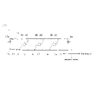
specifically, as shown in FIG. 5, each of the light emitting elements 30 which
is
die-bonded on the wiring portion 12 or the terminal portion 13 (an example of
first
wiring portion) is electrically connected to the wiring portion 12 or the
terminal portion
13, to which the light emitting element 30 is die bonded respectively, through
a wire
Wl, and is electrically connected to adjacent wiring portion 12 or terminal
portion 13
(an example of second wiring portion) through a wire W2. In this case, it is
preferable
that the wire W2 is bonded to the wiring portion 12 or the terminal portion 13
to which
the light emitting element 30 is die bonded, and bridging over the third
groove portion
143, is bonded to adjacent wiring portion 12 or the terminal portion 13. Also,
the wire
W2 is preferably connected to the light emitting element 30 along the second
direction
(that is along the lateral direction). With the wire W2 arranged along the
second
CA 02833466 2013-11-15
direction, in the case where the substrate member 10 is bent, occurrence of
problems
such as disconnection of the wire W2 due to the stress experienced on the wire
W2 can
be prevented. As described above, in the case where mounting is performed by
way of
wire bonding, the sealing member 20 preferably covers the wire W2 in addition
to the
light emitting element 30. With this arrangement, problems such as
disconnection of
the wire W2 can be prevented.
[0053] (9) In the above-described embodiment, three groove portions 14 are
arranged
spaced apart from one other when viewed from the second direction, but not
limited
thereto. For example, as shown in FIG. 5, adjacent groove portions 14 may be
arranged overlapping with each other when viewed from the second direction.
[0054] (10) In the above-described embodiment, the third groove portion 143 of
the
groove portion 14 is disposed at a center portion in the second direction of
the light
emitting device 100, but not limited thereto. For example, as shown in FIG. 5,
the
third groove portion 143 may be disposed at a location a predetermined
distance from
the center portion in the second direction of the light emitting device 100.
In this case,
the light emitting device 30 is preferably disposed at a center portion in the
second
direction of the light emitting device 100.
[0055] (11) In the above-described embodiment, three groove portions 14 have a
same shape, but is not limited thereto. The three groove portions 14 may have
different shapes from each other. More specifically, the angles of the first
groove
portion 141, the second groove portion 142, and the third groove portion 143
with
respect to the first direction may be different in three groove portions 14.
[0056] (12) In the above-described embodiment, a pair of terminal portions 13
are
disposed respectively at the both sides in the first direction of the
plurality of wiring
portions 12, but are not limited thereto. The pair of terminal portions 13 may
be
formed extending in the first direction at the both sides in the second
direction of the
plurality of wiring portions 12. Thus, each of the pair of terminal portions
13 is
formed elongated in the first direction, so that at the time when the
substrate member 10
is bend, stress experienced on the light emitting elements 30 and the sealing
members
20 can be reduced.
[0057] (13) In the above-described embodiment, the light emitting device 100
includes three sets of the groove portion 14, the sealing member 20, and the
light
emitting element 30, but is not limited thereto. The light emitting device 100
may
include four or more sets (for example, 10 sets, 50 sets, 100 sets, or 200
sets) of the
groove portion 14, the sealing member 20, and the light emitting element 30.
That is,
the light emitting device 100 may include four or more sealing members 20 and
four or
11
CA 02833466 2013-11-15
more light emitting elements 30. In this case, the interval between the
sealing
members 20 in the first direction can be, for example, 2 mm, 5 mm, 10 mm, 30
mm, 70
mm, or 100 mm.
[00581 (14) In the above-described embodiment, the first groove portion 141
and the
second groove portion 142 of the groove portion 14 are respectively formed
linearly in
the third direction, but are not limited thereto. The end portions in the
second direction
of the first groove portion 141 and the second groove portion 142 may be
rounded.
With this arrangement, the reflection layer 15 can be prevented from being
damaged by
the corners of the wiring portion 12.
[0059] Further, the groove portion 14 may include a fourth groove portion
disposed
continuous to the first groove portion 141 and at a slanted angle to the first
direction
and/or a fifth groove portion disposed continuous to the second groove portion
142 and
at a slanted angle to the first direction.
[0060] (15) Although specifically described in the above-described embodiment,
the
wiring portion 12 may have a cut-off portion for self-alignment of the light
emitting
element 30. More specifically, as shown in the plan view in FIG. 6, each of
the pair of
wiring portions 12 may have a pair of recessed portions 12a. The bonding
member
105 connecting the light emitting element 30 with a pair of wiring portions 12
is
disposed in the connecting region 12R formed in between the pair of recessed
portions
12a. Thus, the bonding member 105 is held between the pair of recessed
portions 12a
which allows self-alignment of the light emitting elements 30 at respective
predetermined positions. The bonding regions 12R preferably have a width
approximate to the shape of the electrodes of the corresponding light emitting
elements
30, and more preferably have a size approximate to the size of the electrodes.
With the
arrangement described above, preferable self-alignment of the light emitting
elements
30 can be achieved.
[0061] Here, as shown in FIG. 6, the pair of recessed portions 12a are
preferably
formed along the third direction. Thus, the pair of recessed portions 12a are
formed
along a direction intersecting the second direction allows reduction of the
stress
generated by bending the substrate member 10 expressed on the light emitting
elements
30. Also, in
FIG. 6, the bonding regions 12R have a parallelogram shape but the shape
is not limited to this, a rectangular shape or a circular shape may be
employed according
to the shape of the electrodes of the light emitting element.
[0062] (16) In the above-described embodiment, the plurality of light emitting
elements 30 are connected in parallel, but the connection is not limited to
this, an
12
CA 02833466 2013-11-15
appropriate connection such as series connection, series-parallel connection,
parallel-series connection, or the like, can be employed.
[0063] (17) The light emitting elements 30 may be so-called bare chips as
described
above, but chips in which a layer including a wavelength converting member,
and/or a
light-reflecting layer, etc. is previously disposed around such bare chips can
also be
used.
[0064] (18) In the above-described embodiment, the sealing members 20 are
disposed only over the third groove portions 143 and spaced apart from the
first groove
portions 141, which is preferable for protection of the sealing member 20, but
the
arrangement is not limited to this. That is, the sealing members 20 may be
disposed,
each extending over the corresponding first and second groove portions.
[0065] (19) In the above-described embodiment, the third groove portions 143
are
formed at the same positions in the second direction (in the same straight
line along the
first direction), but the arrangement is not limited to this. That is, in the
case where a
plurality of third groove portions are formed, the third groove portions may
be located
at different positions in the second direction.
[0066] As described above, it should be obvious that various other embodiments
are
possible without departing the spirit and scope of the present invention.
Accordingly,
the scope and spirit of the present invention should be limited only by the
following
claims.
13