Note : Les descriptions sont présentées dans la langue officielle dans laquelle elles ont été soumises.
CA 02833862 2013-11-19
e
,
PASSIVELY VARIABLE EMITTANCE DEVICE AND METHOD FOR MAKING
THE SAME
TECHNICAL FIELD
The present invention relates to the field of variable emittance devices, and
more
particularly to passively variable emittance devices.
BACKGROUND
Satellites in orbit encounter quite large temperature variations depending of
their exposure
to the solar energy. However, their internal temperature should be controlled
to an optimal
operating temperature range in order to keep all the electronic systems
function under
stabilized conditions.
Radiators are usually used for maintaining the internal temperature of a
satellite within the
optimal operating temperature range. The heat exchange between the radiator
and its
environment is mainly controlled through radiation, which is in turn
determined by the
radiator emittance. Therefore, the thermal control of the satellite internal
temperature may
be achieved via the use of a radiator having variable emittance surfaces. By
adapting the
emittance value to the external temperature, it is possible to radiate more or
less heat so that
a control of the temperature of the satellite is achieved.
There are mainly two types of radiators used for the thermal control systems
of satellites, i.e.
active and passive approaches. The active approach includes all the thermal
management
systems that are activated electrically. One example of an active radiator
consists in an
active thermal control system comprising electro-mechanical louvers formed of
highly
reflective metal blades which open and close depending on the external
temperature to
expose more or less area of an emissive surface. The control of the electro-
mechanical
louvers requires temperature sensors, power supply and control circuits, which
makes them
complex, expensive, and/or bulky.
A passive radiator is a passive variable emittance device comprising a coating
having an
emittance that can self-adjust with the temperature. For example, it has been
reported in the
- 1 -
CA 02833862 2013-11-19
prior art that coatings made of lanthanum-strontium-manganate may present a
change in the
emittance from 0.37 to 0.67 while the temperature increasing from 220K to
340K. However,
the maximum emittance at high temperature, i.e. 0.67, may not be sufficient
for evacuating
heat.
Therefore, there is a need for an improved passive variable emittance device
having
applications in at least the field of satellites.
SUMMARY
According to a broad aspect, there is provided a passive variable emittance
device
comprising: a substrate having a receiving surface adapted to reflect
radiations having a
given wavelength; an intermediary layer deposited on the receiving surface of
the substrate
and being substantially transparent to the radiations having the given
wavelength; and a
thermochromic layer deposited on top of the intermediary layer, the
thermochromic layer
being substantially transparent to the radiations having the given wavelength
for a first
temperature below a given transition temperature, and presenting both
reflection and
absorption for the radiations for a second temperature above the given
transition
temperature, a total optical thickness for the intermediary and thermochromic
layers being
substantially equal to one quarter of the given wavelength so that radiations
reflected by the
thermochromic layer at the second temperature destructively interfere with
radiations
transmitted by the thermochromic and intermediary layers and reflected by the
substrate in
order to obtain a first emittance for the passive variable emittance device at
the second
temperature being greater than a second emittance for the passive variable
emittance device
at the first temperature.
In one embodiment, a physical thickness of the thermochromic layer is
comprised between
about 10 nm and about 80 nm.
In the same or another embodiment, a physical thickness of the intermediary
layer is greater
than about 1
In one embodiment, an optical thickness of the thermochromic layer is
substantially
negligible relative to an optical thickness of the intermediary layer, a
physical thickness of
- 2 -
CA 02833862 2013-11-19
the intermediary layer being substantially equal to one quarter of the given
wavelength in
the intermediary medium.
In one embodiment, the receiving surface of the substrate is adapted to
reflect an infrared
light, the intermediary layer is made of a material that is substantially
transparent to the
infrared light, and the thermochromic layer is made of a material that is
substantially
transparent to the infrared light, when in a semiconductor state, and that
both reflects and
absorbs the infrared light when in a metallic state.
In one embodiment, the receiving surface of the substrate is made of a
material selected
from a group consisting of: gold, aluminum, platinum, copper, silver, zinc,
and alloys
thereof.
In one embodiment, the intermediary layer is made of a material selected from
a group
consisting of: Si02, A1203, MgO, Ta205, ZnO, Zr02, Ti02, CaF2, ThF4, Si3N4,
Boron
Silicate Crown glass BK7, ZnS, and ZnSe.
In one embodiment, the thermochromic layer is made of a material selected from
a group
consisting of: V02, V407, V6011, V203, V509, V6013, VO, V8015, V205, Fe304,
Nb02, NiS, Ti203, Ti305, Ti407, Ti509, SmNi03, LaCo03, NdNi03, and PrNi03.
In one embodiment, the passive variable emittance device is adapted to be used
as a radiator
for a satellite.
In another embodiment, the passive variable emittance device is adapted to be
used as a
temperature-controlled optical switch.
According to another broad aspect, there is provided a method for making a
passive variable
emittance device, comprising: providing a substrate having a receiving surface
adapted to
reflect radiations having a given wavelength; depositing an intermediary layer
on the
receiving surface of the substrate, the intermediary layer being substantially
transparent to
the radiations having the given wavelength; and depositing a thermochromic
layer on top of
the intermediary layer, the thermochromic layer being substantially
transparent to the
radiations having the given wavelength for a first temperature below a given
transition
-3 -
CA 02833862 2013-11-19
temperature, and presenting both reflection and absorption for the radiations
for a second
temperature above the given transition temperature, a total optical thickness
for the
intermediary and thermochromic layers being substantially equal to one quarter
of the given
wavelength so that radiations reflected by the thermochromic layer at the
second
temperature destructively interfere with radiations transmitted by the
thermochromic and
intermediary layers and reflected by the substrate in order to obtain a first
emittance for the
passive variable emittance device at the second temperature being greater than
a second
emittance for the passive variable emittance device at the first temperature.
In one embodiment, the step of depositing a thermochromic layer comprises
depositing a
thermochromic layer having a physical thickness comprised between about 10 nm
and
about 80 nm.
In the same or another embodiment, the step of depositing an intermediary
layer comprises
depositing an intermediary layer having a physical thickness greater than
about 1 m.
In one embodiment, the optical thickness of the thermochromic layer is
substantially
negligible relative to the optical thickness of the intermediary layer, the
physical thickness
of the intermediary layer being substantially equal to one quarter of the
given wavelength in
the intermediary medium.
In one embodiment, the receiving surface of the substrate is adapted to
reflect an infrared
light, the intermediary layer is made of a material that is substantially
transparent to the
infrared light, and the thermochromic layer is made of a material that is
substantially
transparent to the infrared light, when in a semiconductor state, and that
both reflects and
absorbs the infrared light when in a metallic state.
In one embodiment, the receiving surface of the substrate is made of a
material selected
from a group consisting of: gold, aluminum, platinum, copper, silver, zinc,
and alloys
thereof.
In one embodiment, the intermediary layer is made of a material selected from
a group
consisting of: Si02, A1203, MgO, Ta205, ZnO, Zr02, Ti02, CaF2, ThF4, Si3N4,
Boron
Silicate Crown glass BK7, ZnS, and ZnSe.
- 4 -
CA 02833862 2013-11-19
In one embodiment, the thermochromic layer is made of a material selected from
a group
consisting of: V02, V407, V6011, V203, V509, V6013, VO, V8015, V205, Fe304,
Nb02, NiS, Ti203, Ti305, Ti407, Ti509, SmNi03, LaCo03, NdNi03, and PrNi03.
In one embodiment, the passive variable emittance device is adapted to be used
as a radiator
for a satellite.
In another embodiment, the passive variable emittance device is adapted to be
used as a
temperature-controlled optical switch.
In the below description, the emittance refers to the ratio of the amount of
heat radiated by a
surface area to the amount of heat radiated by the blackbody at the same
temperature.
BRIEF DESCRIPTION OF THE DRAWINGS
Further features and advantages of the present invention will become apparent
from the
following detailed description, taken in combination with the appended
drawings, in which:
Fig. 1 is a passive variable emittance device, in accordance with an
embodiment;
Fig. 2a schematically illustrates an operation principle of the passive
variable emittance
device of Fig. 1 when at a temperature below a transition temperature;
Fig. 2b schematically illustrates an operation principle of the passive
variable emittance
device of Fig. 1 when at a temperature above a transition temperature;
Fig. 3a is a graph of a reflectance as a function of wavelength for a
simulated passive
variable emittance device operated at a temperature below a transition
temperature;
Fig. 3b is a graph of a reflectance as a function of wavelength for the
simulated passive
variable emittance device of Fig. 3a operated at a temperature above a
transition
temperature;
Fig. 4 is a schematic illustration of a pulsed laser deposition setup, in
accordance with an
embodiment;
- 5 -
CA 02833862 2013-11-19
Fig. 5 is an exemplary graph of a resistivity of a V02 film as a function of
temperature;
Fig. 6 is an exemplary graph of a reflectivity of a V02 film as a function of
wavelength for
different temperatures;
Fig. 7a is an exemplary graph of a reflectance of a passive variable emittance
device
comprising a 1340nm physical thickness Si02 layer as a function of wavelength
for
different V02 layer physical thicknesses and for a temperature below a
transition
temperature;
Fig. 7b is an exemplary graph of a reflectance of the passive variable
emittance device of
Fig. 7a as a function of wavelength for different V02 layer physical
thicknesses and for a
temperature above a transition temperature;
Fig. 8 is an exemplary graph of an emittance of a passive variable emittance
device
comprising a 1340nm physical thickness Si02 layer as a function of a physical
thickness of
a V02 layer for temperatures above and below the transition temperature of V02
as well as
the corresponding tunability of the emittance (i.e. the emittance above the
transition
temperature minus the emittance below the transition temperature);
Fig. 9a is an exemplary graph of a reflectance of a passive variable emittance
device
comprising a 30 nm physical thickness V02 layer as a function of wavelength
for different
transparent Si02 layer physical thicknesses and for a temperature below a
transition
temperature;
Fig. 9b is an exemplary graph of a passive variable emittance device
comprising a 30 nm
physical thickness V02 layer as a function of wavelength for different
transparent Si02
layer physical thicknesses and for a temperature above a transition
temperature;
Fig. 10 is an exemplary graph of an emittance of a passive variable emittance
device
comprising a 30 nm physical thickness V02 layer as a function of a physical
thickness of a
transparent Si02 layer for temperatures above and below the transition
temperature of V02
as well as the corresponding tunability of the emittance (i.e. the emittance
above the
transition temperature minus the emittance below the transition temperature);
- 6 -
CA 02833862 2013-11-19
Fig. 11 is an exemplary graph of an emittance of a passive variable emittance
device
comprising a 30 nm physical thickness V02 layer and a 1360 nm physical
thickness Si02
layer as a function of the temperature; and
Fig. 12 is an exemplary graph of an emittance of a passive variable emittance
device
comprising a 2.5% tungsten-doped V02 layer with a physical thickness of about
30 nm and
a Si02 layer with a physical thickness of about 1360 nm as a function of the
temperature.
It will be noted that throughout the appended drawings, like features are
identified by like
reference numerals.
DETAILED DESCRIPTION
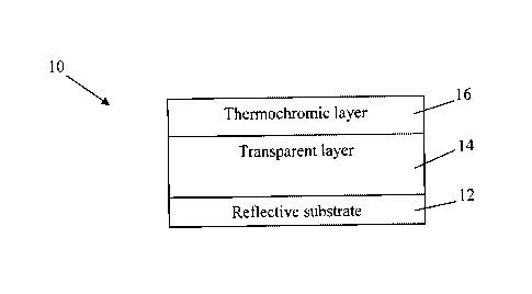
Figure 1 illustrates one embodiment of a passive variable emittance device 10
comprising
three layers 12, 14, and 16. The passive variable emittance device 10 presents
an emittance
that increases while its temperature increases. As a result, the passive
variable emittance
device 10 presents a substantially low emittance at substantially low
temperatures and a
substantially high emittance at substantially high temperatures.
The layer 12 comprises a reflecting substrate adapted to reflect radiations
having a given
wavelength in vacuum. The reflecting substrate 12 can comprise a single layer
made of a
reflective material adapted to reflect the radiations having the given
wavelength in vacuum.
Alternatively, the reflecting substrate 12 can comprise two layers, i.e. a
first layer made of a
non-reflective material and a second layer deposited on top of the first layer
and made of a
reflective material adapted to reflect the radiations having the given
wavelength in vacuum.
It should be understood that in the following description, the term
"wavelength" refers to a
wavelength in vacuum unless identified differently. The layer 14 is deposited
on a receiving
surface of the reflecting substrate 12 and is made of a material that is
substantially
transparent to the radiations having the given wavelength. The layer 16 is
deposited on the
substantially transparent layer 14 so that the substantially transparent layer
14 is sandwiched
between the reflecting substrate 12 and the layer 16. The layer 16 is made of
a
thermochromic material that presents a reversible semiconductor-to-metal
transition when
the temperature is increased, and reversible metal-to-semiconductor transition
when the
- 7 -
CA 02833862 2013-11-19
temperature is decreased. When the temperature of the thermochromic material
is below the
transition temperature Tt of the thermochromic material, the thermochromic
material is in a
semiconductor or insulator state while it is in a metallic state when its
temperature is above
the transition temperature Tt. As a result, the optical and electrical
properties of the
thermochromic layer 16 vary as a function of the temperature thereof.
Particularly, the
thermochromic layer 16 is substantially transparent to the radiations having
the given
wavelength when the temperature of the thermochromic material is below the
transition
temperature Tt. When the temperature of the thermochromic material is above
the transition
temperature Tt, the thermochromic material presents both reflection and
absorption for the
radiations having the given wavelength.
As described below, the physical thicknesses of the transparent layer 14 and
the
thermochromic layer 16 are chosen so that the passive variable emittance
device 10 operates
as a reflector for temperatures below the transition temperature Tt, and as a
heat emitter, via
generation of destructive interferences, for temperatures above the transition
temperature Tt.
The physical thickness of the thermochromic layer 16 is chosen so as to be
transparent when
its temperature is below the transition temperature Tt, and so that both
reflection and
absorption of radiation by the thermochromic layer 16 occurs when the
temperature is above
the transition temperature Tt. If the physical thickness of the thermochromic
layer 16 is too
small, the major part of the incident radiation at high temperature propagates
therethrough
and is then reflected back by the reflecting substrate 12 through the layers
14 and 16,
resulting in a low value of emittance at high temperature. On the other hand,
if the physical
thickness of the thermochromic layer 13 is too large, the radiation at high
temperature is
simply reflected by the thermochromic layer 16 and substantially no radiation
propagates
therethrough, resulting also in a low emittance value at high temperature. In
one
embodiment, the physical thickness of the thermochromic layer is comprised
between
about 10 nm and about 80 nm.
In one embodiment, the physical thickness of the thermochromic layer 16 is
chosen so that,
when the temperature of the thermochromic layer is above the transition
temperature Tt, the
amount of radiation reflected by the thermochromic layer 16 is substantially
equal to the
- 8 -
CA 02833862 2013-11-19
amount of radiation reflected by the reflecting substrate 12 and exiting the
passive variable
emittance device 10.
Furthermore, the total optical thickness of the transparent layer 14 and the
thermochromic
layer 16 is chosen so as to be substantially equal to the quarter of the given
wavelength of
the radiation in vacuum so as to allow the generation of destructive
interferences when the
temperature of the thermochromic layer 16 is above the transition temperature
Tt.
The person skilled in the art will understand the optical thickness of a layer
made of a given
material is equal to the refractive index of the given material multiplied by
the physical
thickness of the layer. Similarly, the wavelength of a given radiation
propagating in a given
material is equal to the wavelength of the radiation in vacuum divided by the
refractive
index of the material.
In one embodiment, the optical thickness of the thermochromic layer 16 is
negligible
relative to that of the transparent layer. For example, the optical thickness
of the
thermochromic layer 16 may be considered as negligible relative to that of the
transparent
layer when the corresponding physical thickness of the thermochromic layer 16
is about 10
times less than the corresponding physical thickness of the transparent layer.
In this case, the
optical thickness of the transparent layer 14 may be chosen to be
substantially equal to the
quarter of the given wavelength of the radiation in vacuum. In other words,
the physical
thickness of the transparent layer 14 may be chosen to be substantially equal
to the quarter
of the given wavelength of the radiation in the transparent medium.
In one embodiment, the physical thickness of the transparent layer 14 is
greater than about 1
ttm.
Figures 2a and 2b illustrate the operation principle of the passive variable
emittance
device 10 when its temperature is below and above the transition temperature
Tt,
respectively.
When the temperature of the thermochromic layer 16 is below the transition
temperature Tt,
the thermochromic layer is in its semiconductor state and both the
thermochromic layer 16
and the transparent layer 14 are substantially transparent to the radiations
having the given
- 9 -
CA 02833862 2013-11-19
wavelength. As a result, by assuming a near-normal incidence, an incident
radiation 20
having the given wavelength propagates through the two layers 14 and 16 before
reaching
the reflecting substrate 12. For example, an incident radiation 20 may be
considered as
being "near-normal", when the angle between the incident radiation 20 and the
normal to the
surface of the thermochromic layer 16 is less than about 30 degrees or
substantially equal to
about 30 degrees. The incident radiation 20 is then reflected, thereby
generating the
reflected radiation 22 which propagates through the transparent and
thermochromic
layers 14 and 16 in order to exit the passive variable emittance device 10. As
a result, most
of the incident radiation is reflected by the passive variable emittance
device 10.
When the temperature of the thermochromic layer 16 is above the transition
temperature Tt,
i.e. when the thermochromic material is in the metallic state, the
thermochromic layer 16
both reflects and propagates radiation. As illustrated in Figure 2b, an
incident radiation 20
having a "near-normal incidence" is divided into a reflected radiation 24 and
a propagating
radiation 26 that propagates through the thermochromic layer 16 and the
transparent
layer 14. It should be understood that some of the propagating radiation is
absorbed by the
thermochromic material. The radiation 26 is reflected back by the reflecting
substrate 12 and
the reflected radiation 28 propagates through the transparent layer 14 towards
the
thermochromic layer 16. A first part of the reflected radiation 28 is
reflected at the interface
between the transparent layer 14 and the thermochromic layer 16 and propagates
back
towards the reflecting substrate 12. The second part of the reflected
radiation 28 propagates
through the thermochromic layer 16 and exits the passive variable emittance
device 10. It
should be understood that further internal reflections of the radiation may
occur, and for
each reflection at the interface between the transparent and thermochromic
layers some
radiation propagates through the thermochromic layer 16 and exits the passive
variable
emittance device 10. The radiation is substantially attenuated on each
reflection.
Since the total optical thickness of the transparent and thermochromic layers
14 and 16 is
substantially equal to about the quarter of the given wavelength of the
radiation, the
radiation 30 experiences a phase shift of about r with respect to the
radiation 24 reflected by
the thermochromic layer 16. As a result, the phase difference between the
radiation 24
reflected by the thermochromic layer 16 and the radiation 30 reflected by the
reflecting
- 10-
CA 02833862 2013-11-19
substrate 12 is substantially equal to about a, and the radiations 24 and 30
substantially and
destructively interfere together, resulting in a substantially low reflectance
value and a
substantially high emittance value for the passive variable emittance device
10.
In an embodiment in which the physical thickness of the thermochromic layer 16
is chosen
so that the amount of radiation reflected by the thermochromic layer 16 is
substantially
equal to the amount of radiation reflected by the reflecting substrate 12 and
exiting the
passive variable emittance device 10, when the temperature is above the
transition
temperature Tt, substantially no radiation having the given wavelength is
reflected by the
passive variable emittance device 10.
While in the present description, it is referred to a given wavelength for the
radiation, the
person skilled in the art will understand that the passive variable emittance
device 10 is
adapted to selectively reflect radiations having a wavelength included in a
wavelength band
containing the given wavelength and emit heat. In one embodiment, the
wavelength band is
substantially centered on the given wavelength.
In one embodiment, the passive variable emittance device 10 is designed for
selectively
reflecting infrared radiations or light and emitting heat. In this case, the
reflecting
substrate 12 is made of a material adapted to reflect infrared light, the
transparent layer is
made of a material that is substantially transparent to infrared light, and
the thermochromic
layer 16 is made of a material that is substantially transparent to infrared
light, when in its
semiconductor state, and that both reflects and absorbs infrared light when in
its metallic
state.
In this case, the reflecting substrate 12 may be made of a metallic material
such as gold,
aluminum, platinum, copper, silver, zinc, alloys thereof, or the like. In
another embodiment,
the reflecting substrate may be made of a non-reflecting material having a
reflecting coating
thereon.
The transparent layer 14 may be made from a dielectric material transparent to
infrared
light. Oxides such as Si02, A1203, MgO, Ta205, ZnO, Zr02, Ti02, or the like
may be
used. In another example, fluorides such as CaF2, ThF4, or the like may be
used. In a
- 11 -
CA 02833862 2013-11-19
further example, nitrides such as Si3N4, or any other adequate dielectric
material such as
Boron Silicate Crown glass BK7, ZnS, ZnSe, void, or the like may be used.
In one embodiment, the thermochromic layer 12 is made from vanadium dioxide
V02. It
should be understood that the vanadium dioxide may be crystalline or
polycrystalline.
Vanadium dioxide exhibits one of the largest observed variations in the
electrical and
optical properties due to a reversible semiconductor-to-metal transition that
occurs at a
transition temperature Tt of about 68 C, which is close to room temperature.
From an
optical point of view, vanadium dioxide presents a good transparency to
infrared radiation in
the semiconductor (or insulator) state, and both its absorption and reflection
are increased by
increasing the temperature above Tt. Moreover, the transition temperature Tt
of vanadium
dioxide can be lowered through doping with donors, such as W or Mo, or raised
through
doping with acceptors, such as Ti or Al. BY adequately choosing an appropriate
dopant and
its quantity, it is possible to obtain a precise control of the transition
temperature Tt, for
instance around room temperature.
In another embodiment, the thermochromic layer may be made of a material such
as V407,
V6011, V203, V509, V6013, VO, V8015, V205, Fe304, Nb02, NiS, Ti203, Ti305,
Ti407, Ti509, SmNi03, LaCo03, NdNi03, PrNi03, or the like.
In one embodiment, the passive variable emittance device 10 comprises a layer
of Si02
having a physical thickness greater than about 1 1AM and a layer of vanadium
dioxide having
a physical thickness comprised between about 10 nm and about 80 nm.
In one embodiment, the passive variable emittance device 10 is used as a
radiator for
satellites. In this case, the layers characteristics may be chosen to obtain
the interferences in
the thermochromic metallic state for a given range of wavelengths in the mid-
infrared range,
around the maximum of the blackbody at a desired operating temperature for the
components of the satellite, e.g. room temperature. For example, the range of
wavelength
may be centered around about 7.7 1.1m, which corresponds to the maximum of the
blackbody
at 100 C. In this case, the optical thickness of the thermochromic layer 16
may be
negligible with respect to that of the transparent layer 14 made of CaF2 for
example, which
may be substantially equal to about 1.925 pm (= 7.7 p.m / 4). The
corresponding physical
- 12 -
CA 02833862 2013-11-19
thickness of CaF2 may be substantially equal to about 1.426 um (= 1.925 j.tm /
nCaF29
with nce2= 1.35).
In another embodiment, the passive variable emittance device 10 is used as a
temperature-
controlled switch. An incident light beam having a given wavelength is
propagated on the
thermochromic layer 16 of the passive variable emittance device 10. When the
temperature
of the thermochromic layer 16 is below the transition temperature Tt, the
incident light
beam propagates through the transparent and thermochromic layers 14 and 16
before being
reflected by the reflecting layer 12 and propagating back through the
transparent and
thermochromic layers 14 and 16. The incident light beam is then reflected by
the passive
variable emittance device 10. When the temperature of the thermochromic layer
16 is
increased above the transition temperature Tt, destructive interferences
occurs, as explained
above, and substantially no light beam is reflected by the passive variable
emittance
device 10.
Figures 3a illustrates the simulated reflectance for a passive variable
emittance device
comprising a 20 nm physical thickness V02 thermochromic layer and a 1300 nm
physical
thickness Si02 transparent layer on a gold substrate, for a temperature below
the transition
temperature Tt. One can note that the reflectance is high (i.e.> about 0.6)
over a wide range
(i.e. from about 2.5 pm to about 15 um) of infrared wavelengths, except for
some absorption
bands of Si02 such as a first band at about 2.5 um to about 4 p.m, a second
band at about 8
p.m to about 8.5 gm, a third band at about 9 p.m to about 10 um, and a fourth
band around
about 12.5 [um
Figure 3b illustrates the simulated reflectance for the passive variable
emittance device of
Figure 3a and for a temperature greater than the transition temperature Tt of
the
thermochromic layer. One can note that the reflectance is considerably
decreased over a
wide range of infrared wavelengths with respect to that of Figure 3a.
The skilled person will understand that if the physical thickness of the V02
layer is too
small, the major part of the incident radiation at high temperature will pass
through the V02
film and be then reflected back by the substrate. In this case, the
interference effect will be
too small to achieve high emittance values at high temperature. The optimal
physical
- 13 -
= CA 02833862 2013-11-19
thickness of the V02 layer should be experimentally determined, depending on
the
properties of the V02 film, such as its density and its roughness for example.
A further increase in the physical thickness of the V02 layer will increase
the absorption
effect of the device to the detriment of the interference effect. In fact, for
thicker V02 film,
the radiation transmitted through the thin V02 thermochromic layer is
attenuated and then
reflected by the back infrared high-reflecting substrate. The reflected
radiation is further
attenuated while propagating through the V02 layer after being reflected by
the reflecting
substrate.
Therefore, a further increase in the physical thickness of the V02 layer will
increase its
reflectivity at high temperature and completely suppress the transmittance,
resulting in a
decrease of the emittance for the passive variable emittance device with
increasing the
temperature, which is a common behavior for V02 films deposited on infrared
low-
reflecting substrates, namely high emittance at low temperature, and low
emittance at high
temperature. In this case, the passive variable emittance device is no longer
suitable for
radiator applications.
The passive variable emittance device 10 may be made using any adequate
fabrication
technique. A reflective substrate 12 adapted to reflect radiations having a
given wavelength
is provided. The reflecting substrate 12 has a receiving surface on which a
transparent
layer 14 made of a material substantially transparent to the given wavelength
is deposited.
Then a thermochromic layer 16 is deposited on top of the transparent layer 14
so that the
transparent layer be sandwiched between the reflecting substrate 12 and the
thermochromic
layer 16.
The following presents one exemplary experimental method for depositing a V02
thermochromic layer on a substrate.
The substrates used for the optimization of the electrical and optical V02
properties are:
silicon wafers, Si02/Si, and quartz. The substrates are cleaned ultrasonically
successively in
acetone, isopropyl alcohol (IPA), methanol, and deionized water and then dried
under N2
flow.
- 14 -
CA 02833862 2013-11-19
Figure 4 illustrates a schematic of a Pulsed Laser Deposition (PLD) setup used
for
depositing the different layers on the substrates. The PLD vacuum chamber is
evacuated to
about 10-6 TO1T at room temperature.
The vanadium target is then cleaned using KrF excimer laser (X, = about 248
nm) at a laser
energy density of about 2 J/cm2 with an impulse frequency of about 10 Hz under
vacuum at
room temperature.
For a substrate temperature higher than about 400 C, KrF excimer laser is used
to deposit
vanadium dioxide (V02) films on the Si, Si02/Si and quartz substrates at a
laser energy
density of about 2 J/cm2 under an 02 pressure from about 2 mTorr to about 25
mTorr
(about 2, about 5, about 10, about 15, about 20, and about 25 mTorr) with an
impulse
frequency of about 10 Hz. The distance between the target and the substrate is
kept at
about 6.5 cm. At the end of the pulsed laser ablation process, the samples are
cooled down
to room temperature.
The microstructure of the V02 thin films deposited using reactive pulsed laser
deposition
(RPLD) using vanadium target was confirmed by X-ray diffraction (XRD) for all
the
aforementioned 02 pressures. However, the resistivity measurements carried out
using
conventional four-point probe method revealed that the best resistivity switch
is observed
for the V02 film deposited under a pressure of about 15 mTorr of 02. In fact,
the V02 film
deposited under about 15 mTorr of 02 presents a drop in the resistivity of
about 3.4 orders
of magnitude when the V02 switches to the metallic state, as illustrated in
Figure 5.
Reflectivity measurements in the mid-infrared range were carried out to
identify the optical
switching properties across the metal-to-insulator transition for an about 220
nm physical
thickness V02 film deposited on a quartz substrate at about 15 mTorr 02. As
illustrated in
Figure 6, the spectral reflectivity of the film shows an important variation
across the metal-
to-insulator transition temperature (TMIT) in the mid-infrared range.
While in the above description PLD is used for the deposition of a V02 film,
it should be
understood that other adequate deposition techniques may be used. For example,
sputtering
or sol-gel methods may be used for depositing the V02 film.
- 15 -
CA 02833862 2013-11-19
In the following, an exemplary method for fabricating a passive variable
emittance device
is presented.
The substrates used for the fabrication of the passive variable emittance
device 10 are: (1)
sputter deposited Au/quartz, (2) sputter deposited Al/quartz substrates and
(3) bulk Al
5 substrates.
The expression "sputter deposited" refers to a layer deposited using
sputtering method. At
least I some instances, the sputtering method presents the advantage of
homogeneity of the
deposited films over large surface area substrates, which may be of interest
for industrial
production. Moreover, the deposition rates of metallic films are relatively
high. Both quartz
10 and Al substrates are cleaned according to the abovementioned cleaning
procedure.
In the present example, any adequate infrared-high reflecting material can be
used as a
substrate (such as gold, aluminum, copper, platinum, or the like), either as a
bulk material or
as a thin film.
Si02 films were prepared using Plasma Enhanced Chemical Vapor Deposition
(PECVD)
from a mixture of SiH4 (about 8.5 sccm)/N20 (about 710 sccm)/N2 (about 161.5
sccm).
The process was conducted at a substrate temperature of about 390 C under a
pressure of
about 500 mTorr with an RF power of about 50 watts.
It should be understood that other deposition methods such as PLD or
sputtering may be
used for depositing the Si02 film on the substrate.
The above-described optimized PLD process, including chamber conditioning,
target
cleaning and V02 deposition, was used to deposit the very-thin V02
thermochromic film.
The deposition time was adjusted to get the desired V02 film physical
thicknesses.
In order to verify experimentally the operation of the device, infrared high-
reflecting films
of Au and Al were used as substrates. Amorphous Si02 and polycrystalline V02
layers
were used as the infrared-transparent and the thermochromic layers,
respectively. Two series
of samples were prepared: the first one consisted of samples with the same
physical
thickness of the Si02 (about 1340 nm) layer and with various V02 layer
physical
- 16-
CA 02833862 2013-11-19
thicknesses (about 10, about 20, about 30, about 40, about 50, about 60, about
80, and
about 100 nm), while the second one consisted of samples with the same V02
layer physical
thickness (about 30 nm) and various Si02 layer physical thicknesses (about
460, about 720,
about 1030, about 1360, and about 1570 nm).
In order to properly describe the operation of the passive variable emittance
device 10 as a
radiator, the emittance of the different devices was computed from reflectance
measurements. In fact, the emittance can be obtained by measuring the
reflectance of the
device. According to Kirchhoff s Law, the spectral emittance ex and spectral
absorptance
of a body are equal at any specified temperature and wavelength at thermal
equilibrium
conditions. From this: ex = ax. Therefore, ex of an opaque material can be
expressed as:
ex=1-px (1)
with px being the spectral total reflectance (including the specular and the
diffuse
components of the reflectance).
The emittance versus temperature was then calculated using the relation:
faili2 EA (T)P(A,T)dA
E = __ A (2)
.1'42 P(A,T)dA
where ex(T) is the spectral emittance and P(.1,T) is the radiation of a
blackbody at
temperature T given by Planck's function for the given wavelength and
temperature,
P(Ä, T) = 27thc21[A5 (ehc / icAT i)] (3)
The total reflectance of the devices for different V02 layer physical
thicknesses at low
(about 25 C) and high temperature (about 100 C) is given in the graph
illustrated at
Figure 7a and Figure 7b, respectively. The corresponding emittance values and
the
tunability of the emittance are presented in Figure 8 as a function of the
physical thickness.
The low temperature reflectance of the device slightly decreases while
increasing the V02
layer physical thickness from about 10 to about 100 nm, due to an increase in
the absorption
of the IR radiation for thicker V02 layers (see Figure 7a). As a result, the
corresponding low
- 17 -
CA 02833862 2013-11-19
temperature emittance increases, as illustrated in Figure 8. However, major
changes occur in
the reflectance at high temperature while increasing the physical thickness of
the V02 layer.
As illustrated in Figure 7b, the aforementioned destructive interference of
the reflectance is
clearly observed for a V02 physical thickness ranging from about 10 nm to
about 40 nm.
However, when the physical thickness of the V02 layer is approximately about
50 nm, the
destructive interference of the reflectance is no longer observed and the low
reflectance
values are mainly due to the abovementioned absorption effect. Further
increase of the V02
physical thickness results in a progressive increase of the reflectance.
According to these results, one can observe that interesting emittance
performances are
obtained in the range about 20 nm - about 40 nm for the V02 physical
thickness,
corresponding to the range of V02 physical thicknesses where the interference
effect is
dominant. The most interesting emittance performance in terms of both high
emittance
values at high temperature and tunability is observed for a V02 physical
thickness of
about 30 nm, for which a near zero reflectance is observed in the infrared
range.
Two observations regarding the determination of the optimal physical thickness
of the V02
layer, for which a high emittance performance of the passive variable
emittance device is
achieved, may be considered:
First, if the V02 layer is rough, an effective mixing of the V02 with air (or
void) over a
certain depth is obtained. The physical thickness of the rough V02 layer may
be increased
to get the same emittance performance as the one of a device using an optimal
physical
thickness of a smooth V02 layer.
Second, the effective mixing of the V02 layer with void is also obtained in
the case of a
layer with low density. In this case, it may also be necessary to increase the
physical
thickness of the porous V02 layer to get the same emittance performance as the
one of a
passive variable emittance device using an optimal physical thickness of a
dense V02 layer.
Figure 9a illustrates the effect of changing the physical thickness of the
infrared-
transparent Si02 layer at low temperature. It should be noted that the
increase in the Si02
- 18 -
CA 02833862 2013-11-19
layer physical thickness is accompanied with a slight increase of the
absorption of the
infrared radiation.
Figure 9b illustrates the effect of changing the physical thickness of the
infrared-
transparent Si02 layer on the position destructive interference of the
reflectance at
about 100 C for the optimal V02 thin film physical thickness, i.e. about 30
nm. The
increase of the physical thickness of the Si02 layer shifts the destructive
interference peak
towards the longest wavelengths. Moreover, the destructive interference
becomes broader,
so that lower reflectance is obtained over wide range of wavelengths, which
results in an
increase of the emittance at high temperature for the optimal physical
thickness of Si02.
The optimal physical thickness of the infrared-transparent layer can be
determined to get
optimal emittance performance in terms of large tunability and high emittance
at high
temperature averaged with the blackbody radiation. The most interesting
performances of
the device in terms of emittance at high temperature as well as the tunability
are achieved
for Si02 physical thickness? about 1 gm, as illustrated in Figure 10.
The evolution of the emittance of the passive variable emittance device
comprising an
about 30 nm physical thickness V02 layer and an about 1360 nm physical
thickness Si02
layer as a function of the temperature is given in Figure 11. The emittance
for the device
passes from 0.35 to 0.81 with increasing the temperature. A modulation of
about 0.46 is
therefore achieved.
In one embodiment, for an optimum operation of the disclosed device as a
thermal
regulating system, the transition temperature Tt should be ideally around room
temperature,
and more preferably, the transition should be tailored over a wide range on
temperatures.
This can be achieved for the case of V02 through doping with donors. In order
to
demonstrate this concept for our device, we used about 2.5% tungsten-doped V02
as the
thermochromic layer instead of pure or undoped V02. The emittance performance
with the
temperature is illustrated in Figure 12. The temperature of the operation of
the device was
reduced and the transition was tailored over a wide range of temperature (from
about -5 to
about 65 C). The modulation depth in the emittance is about 0.43 with the
values of
about 0.37 and about 0.80 at low (about -5 C) and high (> about 65 C)
temperature,
- 19 -
CA 02833862 2013-11-19
respectively. Higher tungsten content would allow getting a transition
centered around room
temperature.
In one embodiment, the present passive variable emittance device is simpler
and easier to be
experimentally achieved than the conventional methods used for the regulation
of the
internal temperature of satellites.
The operation of the present passive variable emittance device is based on the
passive
transition of the thermochromic material, so that there is no need for
additional power as for
the electrochromic transition for example.
In one embodiment, the present passive variable emittance device presents
higher emittance
performance as compared to conventional passive tunable emittance coatings,
especially in
terms of emittance at high temperature and tunability, as demonstrated
experimentally.
In one embodiment, the present passive variable emittance device is
lightweight since it is
based on thin films technology (< about 10g/m2).
In one embodiment, the present passive variable emittance device can be
substantially easily
integrated onto a satellite since it is compatible with Aluminum surfaces and
Optical Solar
Reflectors.
In one embodiment, the present passive variable emittance device is
substantially robust
since no moving parts are required.
The embodiments of the invention described above are intended to be exemplary
only. The
scope of the invention is therefore intended to be limited solely by the scope
of the
appended claims.
- 20 -