Sélection de la langue

Search

Sommaire du brevet 2833980 

Énoncé de désistement de responsabilité concernant l'information provenant de tiers

Une partie des informations de ce site Web a été fournie par des sources externes. Le gouvernement du Canada n'assume aucune responsabilité concernant la précision, l'actualité ou la fiabilité des informations fournies par les sources externes. Les utilisateurs qui désirent employer cette information devraient consulter directement la source des informations. Le contenu fourni par les sources externes n'est pas assujetti aux exigences sur les langues officielles, la protection des renseignements personnels et l'accessibilité.

Disponibilité de l'Abrégé et des Revendications

L'apparition de différences dans le texte et l'image des Revendications et de l'Abrégé dépend du moment auquel le document est publié. Les textes des Revendications et de l'Abrégé sont affichés :

  • lorsque la demande peut être examinée par le public;
  • lorsque le brevet est émis (délivrance).
(12) Brevet: (11) CA 2833980
(54) Titre français: RECEPTEUR DE SIGNAUX RADIOFREQUENCE
(54) Titre anglais: RECEIVER OF RADIO FREQUENCY SIGNALS
Statut: Accordé et délivré
Données bibliographiques
(51) Classification internationale des brevets (CIB):
  • H03G 03/30 (2006.01)
  • H04B 01/16 (2006.01)
(72) Inventeurs :
  • MOIRAGHI, GUIDO (Italie)
  • MOIRAGHI, LUCA (Italie)
  • MOIRAGHI, PAOLO (Italie)
(73) Titulaires :
  • STE INDUSTRIES S.R.L.
(71) Demandeurs :
  • STE INDUSTRIES S.R.L. (Italie)
(74) Agent: ROBIC AGENCE PI S.E.C./ROBIC IP AGENCY LP
(74) Co-agent:
(45) Délivré: 2019-08-27
(86) Date de dépôt PCT: 2012-05-03
(87) Mise à la disponibilité du public: 2012-11-08
Requête d'examen: 2017-04-21
Licence disponible: S.O.
Cédé au domaine public: S.O.
(25) Langue des documents déposés: Anglais

Traité de coopération en matière de brevets (PCT): Oui
(86) Numéro de la demande PCT: PCT/IB2012/052212
(87) Numéro de publication internationale PCT: IB2012052212
(85) Entrée nationale: 2013-10-22

(30) Données de priorité de la demande:
Numéro de la demande Pays / territoire Date
MI2011A000756 (Italie) 2011-05-05

Abrégés

Abrégé français

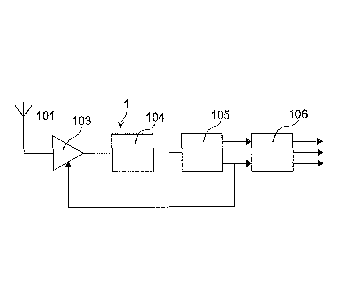
L'Invention concerne un récepteur (1) d'au moins un signal radiofréquence modulé provenant d'une antenne (101) extérieure au récepteur. Le récepteur comprend un premier étage (103) pour l'amplification de bruit faible du signal radiofréquence modulé, et un étage de démodulation (106) dudit signal. Le récepteur comprend un filtre SAW (104) adapté pour agir comme filtre passe-bande autour d'une fréquence prédéterminée pour le signal issu de la première étape; un amplificateur logarithmique (105) adapté pour amplifier le signal issu du filtre SAW; un détecteur de crête (402) du signal de sortie de l'amplificateur logarithmique; un moyen (203) adapté pour commander le gain du premier étage (103) pour l'amplification du signal radiofréquence modulé, en fonction du signal de sortie (Vopeak) du détecteur de crête.


Abrégé anglais

There is described a receiver (1) of at least one radiofrequency modulated signal deriving from an antenna (101) external to the receiver; the receiver comprises a first stage (103) for the low noise amplification of the radiofrequency modulated signal and a demodulation stage (106) of the above-mentioned signal. The receiver comprises a SAW filter (104) adapted to act as a pass band filter about a predetermined frequency for the signal deriving from the first stage, a logarithmic amplifier (105) adapted to amplify the signal deriving from the SAW filter, a peak detector (402) of the output signal of the logarithmic amplifier, means (203) adapted to control the gain of the first stage (103) for the amplification of the radiofrequency modulated signal as a function of the output signal (Vopeak) of the peak detector.

Revendications

Note : Les revendications sont présentées dans la langue officielle dans laquelle elles ont été soumises.


- 8 -
CLAIMS
1. A receiver of at least one radiofrequency modulated signal deriving
from an antenna external to the receiver, said receiver comprising a first
stage
for the low noise amplification of the radiofrequency modulated signal and a
demodulation stage of the radiofrequency modulated signal, characterized by
comprising a Surface Acoustic Wave ("SAW") filter adapted to act as a pass
band filter about a predetermined frequency for the signal deriving from the
first stage for the low noise amplification of the radiofrequency modulated
signal, a logarithmic amplifier adapted to amplify the signal deriving from
the SAW filter, a peak detector of the output signal of the logarithmic
amplifier, means adapted to control the gain of the first stage for the low
noise amplification of the radiofrequency modulated signal as a function of
the output signal of the peak detector, said output signal of the logarithmic
amplifier and said output signal of the peak detector being in input to the
demodulation stage.
2. The receiver according to claim 1, characterized in that said means
are adapted to reduce the gain of the first stage of the low noise
amplification
of the radiofrequency modulated signal in correspondence of a value increase
of the output signal of the peak detector, said means being adapted to
increase the gain of the first stage of amplification of the radiofrequency
modulated signal in correspondence of a value reduction of the output signal
of the peak detector.
3. The receiver according to claim 1, characterized in that said means
comprise a first common emitter bipolar transistor the base terminal of which
is controlled by the output signal of the peak detector, said first
amplification
stage comprising a second common emitter bipolar transistor, the current
flowing through the base terminal of said second bipolar transistor depending
on the current flowing through the collector terminal of the first bipolar
transistor.

- 9 -
4. The receiver according to claim 1, characterized in that said peak
detector comprises at least one capacitor the value of which determines the
decay constant of the output signal of the peak detector.
5. The receiver according to claim 4, characterized in that said peak
detector comprises an operational amplifier having the output signal of the
logarithmic amplifier at the non-inverting input terminal, the output terminal
connected with the anode of a diode having the cathode connected with the
inverting input terminal of the operational amplifier and with one terminal of
a resistance having the other terminal connected with one terminal of said
capacitor having the other terminal connected to a reference voltage.
6. The receiver according to any one of the claims from 1 to 3,
characterized in that said demodulator comprises means adapted to average
the output signal of the logarithmic amplifier, said means comprising at least
a further capacitor.
7. A Low Temperature Cofired Ceramic ("LTCC") package comprising
a receiver as defined in any one of claims 1 to 6 which is manufactured in a
ceramic material substrate and wherein the at least one capacitor and at least
a further capacitor are external to the package.
8. The LTCC package according to claim 7, characterized by comprising
a microcontroller manufactured in said ceramic material substrate, said
receiver being adapted to interact with said microcontroller.

Description

Note : Les descriptions sont présentées dans la langue officielle dans laquelle elles ont été soumises.


CA 02833980 2013-10-22
WO 2012/150565
PCT/1B2012/052212
- I -
Receiver of Radio Frequency Signals
* * * *
DESCRIPTION
The present invention relates to a receiver of radiofrequency signals.
Most of the current receivers of radiofrequency signals use a complex
circuit structure, typically of the superheterodyne type. Said receivers
comprise a mixer, an oscillator for generating the heterodyne signal and a
PLL circuit adapted to stabilize the receiver frequency.
In particular, in the case of devices for transmitting and receiving
information related to some parts of the vehicle, such as for example the
correct level of liquid in a tank, temperature and pressure in a tire, the
battery status and so on, receivers are often integrated in the onboard
computer or located in a more suitable position for receiving signals inside
the vehicle and communicating with the onboard computer. The data
received by the receiver are transmitted to the computer inside the motor
vehicle for displaying simple information messages or alert conditions on a
dedicated display.
However, current receivers are complex especially due to the presence
of a phase detector adapted to compare two signals at different frequencies
and to emit a signal with a phase proportional to the phase difference of the
two signals at different frequencies.
In addition, said receivers absorb significant levels of current and
actuate a consequent energy dissipation.
In view of the prior art, the object of the present invention is to provide
a receiver of radiofrequency signals which is circuit-wise simpler than
known ones and has a lower current absorption than known ones.
According to the present invention, said object is achieved by a
receiver of at least one radiofrequency modulated signal deriving from an
antenna external to the receiver, said receiver comprising a first stage for
the
low noise amplification of the radiofrequency modulated signal and a

CA 02833980 2013-10-22
WO 2012/150565
PCT/1B2012/052212
- 2 -
demodulation stage of the radiofrequency modulated signal, characterized
by comprising a SAW filter adapted to act as a pass band filter about a
predetermined frequency for the signal deriving from the first stage, a
logarithmic amplifier adapted to amplify the signal deriving from the SAW
filter, a peak detector of the output signal of the logarithmic amplifier,
means adapted to control the gain of the first stage for the amplification of
the radiofrequency signal as a function of the output signal of the peak
detector, said output signal of the logarithmic amplifier and said output
signal of the peak detector being in input to the demodulation stage.
, Due to the present invention it is possible to provide a receiver of
radiofrequency signals particularly suitable to be used in short-range data
transmission and reception systems such as car door opening systems or tire
pressure monitoring systems.
The receiver is particularly suitable for receiving signals with pulse
position modulation (PPM) or with pulse width modulation (PWM).
The features and the advantages of the present invention will appear more
clearly from the following detailed description of a practical embodiment
thereof, made by way of a non-limiting example with reference to the
annexed drawings, wherein:
figure 1 shows a block diagram of the receiver of radiofrequency
signals according to the present invention;
figure 2 shows a circuit scheme of the low noise preamplifier stage of
the receiver of figure 1;
figure 3 shows a circuit scheme of the filtering stage of the receiver of
figure 1;
figure 4 shows a diagram of the frequency response of the filtering
stage of figure 3;
figure 5 shows a circuit scheme of the logarithmic amplifier of the
receiver of figure 1;
Figure 6 shows a diagram of the output voltage as a function of the

CA 02833980 2013-10-22
WO 2012/150565
PCT/1B2012/052212
- 3 -
input signal level of the stage in figure 5;
figure 7 shows a circuit scheme of the "ASK" and "PULSE"
comparators used in the receiver of figure 1;
figure 8 schematically shows a package with the receiver of figure 1
made in a substrate of ceramic material according to an embodiment of the
present invention;
figure 9 schematically shows a package with the receiver of figure 1
and a microcontroller made in a substrate of ceramic material according to a
variant of the embodiment of the invention.
With reference to figure 1, there is shown a receiver 1 of
radiofrequency signals according to the present invention. The receiver
comprises a preamplifier stage 103 of a radiofrequency signal received by an
antenna 101, a filtering stage 104, an amplification stage 105 and a signal
demodulation stage 106.
The signal deriving from antenna 101 is at the input to the low noise
preamplifier stage 103 comprising, as better seen in figure 2, a pass band
filter 201 tuned to the reception frequency; the filter 201 also has the
function of impedance adapter.
The output signal of filter 201 is transmitted to a circuit block 202
comprising a radiofrequency transistor Q1 controlled by the output signal to
a circuit 203; the output signal from transistor Q1 flows through a low value
resistance R, preferably about 100 Ohm, such as to have a constant
impedance at the input of the next stage. The transistor Q1 is preferably a
common emitter bipolar transistor. The circuit block 202 represents a low
noise amplifier stage the gain G of which is controlled by the circuit 203.
The circuit 203 is controlled by signal Vopeak deriving from a peak
detector 402 belonging to receiver 1. Circuit 203 comprises a transistor Q2,
preferably a common emitter bipolar transistor with the emitter terminal
connected to-ground GND. The base terminal of transistor Q2 is driven by
signal Vopeak filtered by the low pass filter R70*C50. The signal on the

CA 02833980 2013-10-22
WO 2012/150565
PCT/1B2012/052212
- 4 -
collector terminal of transistor Q2 drives the base terminal of transistor Q1
and varies the base bias current of the transistor Q1 for varying, in
particular
for decreasing, the gain G of transistor Q1 proportionally to the signal
intensity on the antenna; therefore, circuit 203 forms an automatic gain
control block. When the signal Vopeak increases, the transistor Q2 acts so as
to reduce the gain G of the transistor Ql; the gain G of the bipolar
transistor
Q1 is inversely proportional to the amplitude of signal Vopeak.
The output signal of the stage 103 is at the input of a SAW filter 302
of the stage 104, better shown in figure 3, which must select the signals in a
channel between 300 and 600 kHz, i.e. it must filter the signals in a pass
band from 300 to 600 kHz and must ensure a constant group delay time Tg,
where the group delay time indicates the variation of the passage time of a
signal through the pass band Bsaw of the SAW filter. The impedance
adapter circuits 301 and 303, arranged at the input and at the output of the
SAW filter 302, are configured for obtaining a constant group delay time Tg
on the whole pass band Bsaw of the SAW filter 302. Figure 4 shows the
variation of the band and of the group delay time Tg as a function of the
frequency for filter SAW of figure 3. The output signal of filter SAW 302 is
amplified by a fixed gain amplifier 304.
The constancy of the group delay time Tg allows a correct
amplification of the rising and falling edges of the radiofrequency modulated
signal, such as for example when the modulated signal is a signal with pulse
width modulation (PWM) or with pulse position modulation (PPM) where
for example the radiofrequency pulses have rising and falling edges in the
order of 100 nanoseconds.
The output signal of amplifier 304 is at the input of a logarithmic
amplifier 401, shown in figure 5, belonging to stage 105 and adapted to
amplify the input signal. The logarithmic amplifier 401 is a temperature-
compensated amplifier and performs a high gain by the series of multiple
amplification stages Ai...An. Figure 6 shows a diagram of the waveform of

CA 02833980 2013-10-22
WO 2012/150565
PCT/1B2012/052212
- 5 -
the output voltage Vodet as a function of the input signal level In of the
logarithmic amplifier 401 at different frequencies.
The output signal Vodet of the logarithmic amplifier is transmitted to a
demodulation stage for demodulating the information. The same output
signal Vodet of the logarithmic amplifier 401 is transmitted to a peak
detector 402 adapted to detect the peaks of the output signals of the
logarithmic amplifier 401. Preferably, the peak detector 402 comprises an
operational amplifier 403 having the output signal of the logarithmic
amplifier 401 at the non-inverting input terminal, having the output
connected with the anode of a diode 404 having the cathode connected with
the inverting input terminal and with the terminal of a resistance R2 having
the other terminal connected with the terminal of a capacitor Cl in turn
connected to ground GND; the time constant related to capacitor Cl has a
small value, about one microsecond. The voltage Vopeak at the terminals of
capacitor Cl is the output of the peak detector. The output signal Vopeak is
transmitted to a comparator adapted to carry out the signal demodulation and
is used by the circuit 203 for controlling the radiofrequency transistor 202.
The resistance R2 has a low value, preferably 22 Ohm, and serves for
stabilizing the circuit operation compensating the signal propagation delays
by means of the operational amplifier.
Finally, signals Vodet and Vopeak are transmitted to the demodulation
stage 106 for digitally reconstructing the information contained in the
received modulated signal, as better shown in figure 7. The comparator 501
carries out a demodulation in case of signal modulated with amplitude
modulation ASK (Amplitude shift Keying) or also an OOK (On-Off Keying)
modulation; the comparator 501 receives the signal Vodet at the non-
inverting input thereof, while at the inverting input thereof there is the
average value of signal Vodet mediated by a circuit comprising a resistance
R3 connected with a capacitor C2 in turn connected to ground GND and
with the inverting input. The output signal of comparator 501 is the signal

CA 02833980 2013-10-22
WO 2012/150565
PCT/1B2012/052212
- 6 -
Infask. The output signal Vopeak is transmitted as the signal RSSI.
The comparator 502 carries out a demodulation in the case of signal
modulated with pulse position modulation PPM or with pulse with
modulation PWM; the comparator 504 receives the signal Vodet at the non-
inverting input thereof, while at the inverting input thereof there is a
reference signal derived by the resistive divider consisting of resistances R4
and R5 and the signal Vopeak is present across the series of the resistances
R4 and R5. The values of resistances R4 and R5 and of capacitor Cl
determine the decay time constant of the output voltage Vopeak; said time
constant, generally of the order of few milliseconds, takes on a major
importance if the signals received are affected by sudden amplitude
variations, as in the signals used for transmitting the tire pressure. The
output signal of comparator 502 is the signal Infppm. The signals Infask,
Infppm and RSSI are the output signals of the demodulation stage 106 and
of the receiver 1.
In particular, the receiver according to the present invention is more
suitable in data transmission reception systems arranged in vehicles,
preferably motor vehicles. The transmitters may be located in various parts
of the motor vehicle, for example next to the battery or in the tires for
transmitting data on the tire temperature or the tire pressure.
The receiver is adapted to receive said data and transfer them to a
central computer for displaying alarms or messages on a display.
Preferably, in the case of transmission of tire pressure data with pulse
position modulation, the signal transmitted starts after a given period of
time
by the triggering of the oscillations with the generation of a first pulse
that
represents the beginning of the message and has a width W typically of 3
microseconds. Other subsequent pulses are then generated, the temporal
positions thereof, i.e. the periods of time between one pulse and the next
one, represent the content of the information to be transmitted.
The receiver according to the invention is particularly suitable for

CA 02833980 2013-10-22
WO 2012/150565
PCT/1B2012/052212
- 7 -
receiving data modulated according to a pulse position modulation.
According to the invention it is possible to make a package 600, also
called package LTCC, wherein receiver 1 shown in figures 1-6 is made in a
substrate of ceramic material 601 using the LTCC (Low Temperature
Cofired Ceramic) technology, as shown in figure 8. The receiver is
integrally manufactured in the ceramic substrate except for capacitors Cl of
the peak detector 402 and C2 of demodulator 106; said capacitors are
accessible from the outside for adapting the time constants of the peak
detector and of the demodulator to the different requirements of the receiver.
Figure 9 shows a package according to a variant of the embodiment of
the present invention; the package comprises a microcontroller 602 coupled
to the receiver 1 wherein the microcontroller 602 is adapted to manage the
PPM modulated signals received.

Dessin représentatif
Une figure unique qui représente un dessin illustrant l'invention.
États administratifs

2024-08-01 : Dans le cadre de la transition vers les Brevets de nouvelle génération (BNG), la base de données sur les brevets canadiens (BDBC) contient désormais un Historique d'événement plus détaillé, qui reproduit le Journal des événements de notre nouvelle solution interne.

Veuillez noter que les événements débutant par « Inactive : » se réfèrent à des événements qui ne sont plus utilisés dans notre nouvelle solution interne.

Pour une meilleure compréhension de l'état de la demande ou brevet qui figure sur cette page, la rubrique Mise en garde , et les descriptions de Brevet , Historique d'événement , Taxes périodiques et Historique des paiements devraient être consultées.

Historique d'événement

Description Date
Demande visant la révocation de la nomination d'un agent 2023-03-06
Exigences relatives à la révocation de la nomination d'un agent - jugée conforme 2023-03-06
Exigences relatives à la nomination d'un agent - jugée conforme 2023-03-06
Demande visant la nomination d'un agent 2023-03-06
Requête pour le changement d'adresse ou de mode de correspondance reçue 2023-03-06
Lettre envoyée 2023-02-27
Inactive : Certificat d'inscription (Transfert) 2023-02-27
Inactive : Transferts multiples 2023-02-06
Inactive : Demande reçue chang. No dossier agent 2023-02-06
Requête visant le maintien en état reçue 2021-04-28
Inactive : COVID 19 - Délai prolongé 2020-05-28
Inactive : COVID 19 - Délai prolongé 2020-05-14
Requête visant le maintien en état reçue 2020-05-05
Inactive : COVID 19 - Délai prolongé 2020-04-28
Représentant commun nommé 2019-10-30
Accordé par délivrance 2019-08-27
Inactive : Page couverture publiée 2019-08-26
Inactive : Supprimer l'abandon 2019-07-18
Inactive : Lettre officielle 2019-07-18
Inactive : Correspondance - TME 2019-07-08
Inactive : Taxe finale reçue 2019-06-28
Préoctroi 2019-06-28
Inactive : Réponse à l'art.37 Règles - PCT 2019-06-28
Réputée abandonnée - omission de répondre à un avis sur les taxes pour le maintien en état 2019-05-03
Requête visant le maintien en état reçue 2019-04-11
Lettre envoyée 2019-01-11
Un avis d'acceptation est envoyé 2019-01-11
Inactive : Approuvée aux fins d'acceptation (AFA) 2019-01-02
Inactive : Q2 réussi 2019-01-02
Modification reçue - modification volontaire 2018-07-27
Requête visant le maintien en état reçue 2018-03-21
Inactive : Dem. de l'examinateur par.30(2) Règles 2018-02-13
Inactive : Rapport - Aucun CQ 2018-01-31
Lettre envoyée 2017-05-03
Requête d'examen reçue 2017-04-21
Exigences pour une requête d'examen - jugée conforme 2017-04-21
Requête visant le maintien en état reçue 2017-04-21
Toutes les exigences pour l'examen - jugée conforme 2017-04-21
Requête visant le maintien en état reçue 2016-05-02
Requête visant le maintien en état reçue 2015-04-23
Inactive : Page couverture publiée 2013-12-09
Lettre envoyée 2013-12-02
Inactive : Notice - Entrée phase nat. - Pas de RE 2013-12-02
Inactive : CIB en 1re position 2013-11-28
Inactive : CIB attribuée 2013-11-28
Demande reçue - PCT 2013-11-28
Exigences pour l'entrée dans la phase nationale - jugée conforme 2013-10-22
Demande publiée (accessible au public) 2012-11-08

Historique d'abandonnement

Date d'abandonnement Raison Date de rétablissement
2019-05-03

Taxes périodiques

Le dernier paiement a été reçu le 2019-04-11

Avis : Si le paiement en totalité n'a pas été reçu au plus tard à la date indiquée, une taxe supplémentaire peut être imposée, soit une des taxes suivantes :

  • taxe de rétablissement ;
  • taxe pour paiement en souffrance ; ou
  • taxe additionnelle pour le renversement d'une péremption réputée.

Les taxes sur les brevets sont ajustées au 1er janvier de chaque année. Les montants ci-dessus sont les montants actuels s'ils sont reçus au plus tard le 31 décembre de l'année en cours.
Veuillez vous référer à la page web des taxes sur les brevets de l'OPIC pour voir tous les montants actuels des taxes.

Titulaires au dossier

Les titulaires actuels et antérieures au dossier sont affichés en ordre alphabétique.

Titulaires actuels au dossier
STE INDUSTRIES S.R.L.
Titulaires antérieures au dossier
GUIDO MOIRAGHI
LUCA MOIRAGHI
PAOLO MOIRAGHI
Les propriétaires antérieurs qui ne figurent pas dans la liste des « Propriétaires au dossier » apparaîtront dans d'autres documents au dossier.
Documents

Pour visionner les fichiers sélectionnés, entrer le code reCAPTCHA :


Pour visualiser une image, cliquer sur un lien dans la colonne description du document (Temporairement non-disponible). Pour télécharger l'image (les images), cliquer l'une ou plusieurs cases à cocher dans la première colonne et ensuite cliquer sur le bouton "Télécharger sélection en format PDF (archive Zip)" ou le bouton "Télécharger sélection (en un fichier PDF fusionné)".

Liste des documents de brevet publiés et non publiés sur la BDBC .

Si vous avez des difficultés à accéder au contenu, veuillez communiquer avec le Centre de services à la clientèle au 1-866-997-1936, ou envoyer un courriel au Centre de service à la clientèle de l'OPIC.

({010=Tous les documents, 020=Au moment du dépôt, 030=Au moment de la mise à la disponibilité du public, 040=À la délivrance, 050=Examen, 060=Correspondance reçue, 070=Divers, 080=Correspondance envoyée, 090=Paiement})


Description du
Document 
Date
(aaaa-mm-jj) 
Nombre de pages   Taille de l'image (Ko) 
Description 2013-10-21 7 306
Dessins 2013-10-21 4 52
Revendications 2013-10-21 2 84
Abrégé 2013-10-21 1 66
Description 2013-10-22 7 303
Dessin représentatif 2013-12-03 1 4
Revendications 2018-07-26 2 80
Dessin représentatif 2019-07-28 1 3
Paiement de taxe périodique 2024-04-16 6 232
Avis d'entree dans la phase nationale 2013-12-01 1 193
Courtoisie - Certificat d'enregistrement (document(s) connexe(s)) 2013-12-01 1 102
Rappel - requête d'examen 2017-01-04 1 118
Accusé de réception de la requête d'examen 2017-05-02 1 174
Avis du commissaire - Demande jugée acceptable 2019-01-10 1 163
Modification / réponse à un rapport 2018-07-26 8 313
PCT 2013-10-21 11 305
Taxes 2015-04-22 1 52
Paiement de taxe périodique 2016-05-01 1 51
Requête d'examen 2017-04-20 1 55
Paiement de taxe périodique 2017-04-20 1 53
Demande de l'examinateur 2018-02-12 3 158
Paiement de taxe périodique 2018-03-20 2 101
Taxe finale / Réponse à l'article 37 2019-06-27 1 55
Correspondance taxe de maintien 2019-07-07 2 125
Paiement de taxe périodique 2019-04-10 1 46
Courtoisie - Lettre du bureau 2019-07-17 1 26
Paiement de taxe périodique 2020-05-04 2 74
Paiement de taxe périodique 2021-04-27 1 52
Changement No. dossier agent 2023-02-05 34 20 841