Note : Les descriptions sont présentées dans la langue officielle dans laquelle elles ont été soumises.
CA 02834006 2013-11-19
THREE-DIMENSIONAL TITANIA NANO-FIBROUS ARCHITECTURE FOR
MOLECULAR DETECTION BY RAMAN SPECTROSCOPY
FIELD
The present disclosure relate to the fields of molecular detection,
characterization or a combination thereof, using Raman spectroscopy. More
specifically, this disclosure pertains to optical and medical sensor devices
for
detection of analytes that are formed on a titanium substrate, a traditionally
SERS (Surface Enhanced Raman Spectroscopy) inactive material.
BACKGROUND
Testing for substance properties is integral to any science. This step was
traditionally destructive in nature. Examples include pulling a metal apart
until
fracture to determine its strength, combusting a chemical to determine its
elemental composition and digesting food to determine its toxicity. Such
methods
are not practical when considering substances that are expensive, limited in
availability, substantially large or small, statistically variable and those
which can
additionally yield undesirable by-products resulting from destructive testing.
To
that effect, non-destructive testing (NDT) is a widely favored method. One of
the
most powerful NDT techniques is Raman spectroscopy.
Raman spectroscopy is a mature scientific method that can offer
characterization of any substance in any physical state in addition to real-
time
reaction process monitoring. Raman spectroscopy relies on molecular vibrations
that uniquely scatter the incident electromagnetic radiation. Since vibration
is
1
CA 02834006 2013-11-19
highly dependent on boundary constraints, it is possible to characterize
crystal
lattice structures and compositions of matter quite effectively. However, the
scattering intensity due to these molecular vibrations may be too weak to
detect
even with sophisticated Raman equipment. As a result, a constantly increasing
effort is being made to enhance the Raman scattering signal.
To enhance the Raman scattering signal, it was found that the materials'
electronic structure holds most of the potential. That is, the collective
oscillation
or resonance of conductive band electrons can stimulate an electromagnetic
enhancement. It was found that gold (Au) and silver (Ag) possess such
desirable
electronic structures. To localize this resonance condition, it was necessary
to
confine the surface plasmons to features that are smaller than the wavelength
of
incident light (i.e. to nanostructures). As a result, enhancement factors on
the
order of 104 have now become available with Au and Ag nanoparticles (NPs).
The field of study to enhance the Raman spectra is now commonly referred to as
Surface Enhanced Raman Spectroscopy (SERS).
The current state of the art in Raman spectroscopy, as has been for
decades, is to use single Au and Ag nanoparticles to enhance the acquired
spectrum. Well-developed two-dimensional (2-D) nanomanufacturing techniques
have shown Raman enhancement but with drawbacks. For example, recently
published chemical methods to control NP aggregation demand precise solution
control while commonly requiring additional stabilizers to regulate surface
features. Stabilization is even more critical for bigger Au NPs. Modifying the
solution and functionalizing the NPs in this way may also interfere and
mislead
2
CA 02834006 2013-11-19
the acquired Raman spectrum. Consequently, smaller Au NPs are used despite
worse SERS performance. Alternatively, using Ag can improve SERS
performance but the inherent oxide layer causes severe response fluctuations.
Moreover, the highest plasmonic activity of Ag is at around the 532 nm
excitation
wavelength. This regime is highly susceptible to sample fluorescence and
Raman signal deterioration.
Moreover, health and environmental impacts of nanotechnology, to date,
have not been evaluated. This is potentially a serious problem for the future
of
SERS and Raman spectroscopy in general should it become apparent that Au
and Ag NP containing systems are detrimental to human well-beingin which case
new SERS materials would need to be developed. As an alternative, titania is
thermodynamically stable, attracts water and water soluble molecules, it is
favourable for biomolecular bonding and it is corrosion resistant with a
stable
oxide surface. These characteristics are also favourable for SERS since the
system has to remain stable under laser excitation. It is also desired for the
targeted molecules to be in close proximity to the regions of surface enhanced
electromagnetism. In general, titania is already a widely commercially
available
material, being used in cosmetics, pigments, water treatment, solar energy
conversion and ultra-violet ray blocking. Manufacturing benefits such as cost,
sustainability, high production and efficiency may be realized. TiO nanowires
are
already used in some medical devices to enhance surface cellular functions as
disclosed by U.S. Pat. Publication No. 20050221072 and U.S. Pat. Publication
No. 20050038498.
3
CA 02834006 2013-11-19
SUMMARY
The present disclosure teaches how to develop a traditionally SERS
inactive material, titanium, to compete with the enhancement of the most
popular
plasmonic materials used widely in SERS. For example, traditionally SERS
inactive titanium substrate has been developed to compete with the Raman
enhancement of the industry dominant Au and Ag.
The sensor is developed on a titanium substrate using pulsed laser
irradiation to produce a textured surface. The titanium surface, upon being
irradiated by the pulsed laser beam, is partially transformed into titania
micro-
structures and nano-features. This synthesis method may be performed under
ambient conditions in air, or the pressure may be varied from atmosphere. The
synthesis parameters may be varied for sensor performance optimization.
Subsequent application for Raman spectroscopy may make use of single-point,
array, continuous scan or image based irradiation.
An embodiment includes an optical sensor for use with laser excitation
and a Raman spectroscopy detector for detecting the presence of chemical
groups, bio-molecular groups or a combination thereof, when exposed to the
sensor. The sensor includes a titanium substrate, micro-pattern features
developed on the titanium substrate, and three-dimensional nano-structures
that
generally surround and envelop the micro-pattern features. The micro-pattern
features maybe in the form of vias, open channels, enclosed channels,
junctions,
locally oxidized surfaces, or any combination thereof. The nano-structures are
nanofibers.
4
CA 02834006 2013-11-19
In the case of nanofibers as defined in this disclosure, nanoparticles (NPs)
may be spread across the substrate surface and particularly over the "micro-
pattern features" on the substrate in varying degrees of organization and
dimensional structuring. For example, the NPs may be weakly interacting
entities
that are spaced randomly in a single layer. As another example, the NPs may be
strongly interacting entities that form web structures in 3D space. These
aforementioned strong NP interactions are usually not facilitated by any
chemical
additions or reagents but by the laser ablation plasma dynamics as disclosed
herein. The 3D structuring also provides an extra laser confocal volume for
improved detection of chemical compounds. The device is capable of detecting
an analyte with a conservative Raman enhancement factor of up to but not
limited to 106, making it directly competitive to commercial Au and Ag based
SERS devices.
In practicing the disclosed analyte detection method, molecules of the
analyte are exposed to the sensor, the sensor surface is irradiated with a
laser,
and the resulting Raman information is acquired. The Raman equipment may
acquire data from a single irradiated spot. The Raman equipment may also
acquire data from a field of view or a scan that essentially provides spatial
information. Spatial information may be preferred for SERS to reduce the
dependency on regularly ordered "hot-spots" or regions of local
electromagnetic
enhancement. The data acquisition may also repeat in time.
An embodiment provides a method of producing a titanium based Surface
Enhance Raman Scattering (SERS) sensor, comprising:
5
CA 02834006 2013-11-19
providing a titanium substrate having a surface and producing an array of
sensor locations in a predefined portion of the surface by irradiating the
predefined portion of the surface in the presence of air with laser pulses
having
an intensity, a wavelength, a pulse duration, an effective irradiation time
and a
pulse repetition rate selected to produce, at each sensor location, a micro-
pattern
feature in the surface of the substrate and a self-supported web structure
that
generally surround and envelop the micro-pattern feature, said self-supported
web structured being made of nanofibers each comprised of a plurality of
titanium based nanoparticles aligned into said self-supported web structure,
wherein said array of sensor locations exhibit SERS activity.
There is also provided a titanium based Surface Enhance Raman
Scattering (SERS) sensor, comprising:
a titanium substrate having a surface and an array of sensor locations
located in a predefined portion of the surface, each of said sensor locations
including a micro-pattern feature in the surface of the substrate and
nanofibers
that generally surround and envelop the micro-pattern feature, said nanofibers
being comprised of a plurality of titanium based nanoparticles aligned into a
self-
supported web structure, wherein said array of sensor locations exhibit SERS
activity.
There is provided a Raman spectroscopy based method of detecting an
analyte, comprising the steps of:
a) providing a titanium substrate having a surface and producing thereon a
sensor including an array of sensor locations in a predefined portion of the
6
CA 02834006 2013-11-19
surface by irradiating the predefined portion of the surface with laser pulses
having an intensity, a wavelength, a pulse duration, an effective irradiation
time
and a pulse repetition rate selected to produce, at each sensor location, a
micro-
pattern feature in the surface of the substrate and titanium based nanofibers
that
generally surround and envelop the micro-pattern feature, said nanofibers
being
comprised of a plurality of titanium based nanoparticles aligned into a self-
supported web structure, wherein said array of sensor locations exhibit SERS
activity; and
b) exposing said sensor to a sample being tested for the presence of said
analyte and thereafter recording a Raman spectra after irradiating the analyte
sensor with a laser beam and correlating said Raman spectra to a
characteristic
Raman spectra of the analyte to determine the presence or absence of the
analyte in the sample.
There is also provided a titanium based Surface Enhance Raman
Scattering (SERS) system, comprising:
a) a sensor including a titanium substrate having a surface and an array of
sensor locations located in a predefined portion of the surface, each of said
sensor locations including a micro-pattern feature in the surface of the
substrate
and nanofibers that generally surround and envelop the micro-pattern feature,
said nanofibers being comprised of a plurality of titanium based nanoparticles
aligned into a self-supported web structure, wherein said array of sensor
locations exhibit SERS activity;
7
CA 02834006 2013-11-19
b) a sample cell for receiving said sensor, said sample cell being
configured to allow exposure of said sensor to a fluid being tested for the
presence of an analyte;
c) a laser source for illuminating said array of sensor locations with laser
light; and
d) a detector for detecting laser light scattered from said sensor post
exposure of said sensor to said fluid.
A further understanding of the functional and advantageous aspects of the
present disclosure can be realized by reference to the following detailed
description and drawings.
BRIEF DESCRIPTION OF THE DRAWINGS
The embodiments of the present disclosure are described with reference
to the attached figures, wherein:
Figure 1 is a scanning electron microscopy (SEM) image of the 3D titania
nanofibrous network; the particular network shown is generated at a laser
pulse
repetition rate of 13 MHz and an irradiation time of 20 msec; other variations
of
laser repetition rate and irradiation time yield similar SEM images, with
variations
in nanofibrous porosity, 3D network depth and the total affect on the
substrate
(e.g. depth of the micro-vias, micro-via rim height etc.).
Figure 2 is a transmission electron microscopy (TEM) image of the partial
3D titania nanofibrous network that is transferred by electrostatic
interactions to a
TEM grid; the particular network shown is generated at a laser pulse
repetition
8
CA 02834006 2013-11-19
rate of 4 MHz and an irradiation time of lmsec with subsequent irradiation at
26
MHz and 10 msec; other variations of laser repetition rate, irradiation time,
and
subsequent irradiation processing steps yield similar TEM images, with
variations
in nanofibrous aggregation, individual NP size distribution, and length of the
nanofiber segments.
Figure 3 is a non-limiting possibility of the physical layout of one optical
sensor pad; the number of sensor pads on the substrate surface may vary from
one to a plurality thereof and may not necessarily have a square section nor
all
be uniform.
Figure 4 is a non-limiting example of the cross section of the structure of
Figure 3 showing a titanium substrate with micro features produced therein and
nanostructures formed of nanofibers formed on top of the micro features in
which
the nanostructure is shown to be self-supporting in all three rectangular
coordinate dimensions, and the nanofibers may also lay flat on top of the base
sensor surface and are also not necessarily separated uniformly and tend to
arrange in a web-like form as evidenced from the SEM of Figure 1;
Figure 5 is a diagrammatic representation of a non-limiting example of a
nanofiber; the composition and morphology of the nanofiber depends on the
synthesis parameters and experimental conditions as disclosed in this
disclosure;
the nanofiber structure may have all of the features or a selection of more
dominant features; some illustrated nanofiber features may be identified from
the
titania nanofiber TEM image of Figure 2.
9
CA 02834006 2013-11-19
DETAILED DESCRIPTION
Definitions
The terms below have the following meaning in this disclosure, unless
otherwise indicated.
As used herein, the term "analyte" refers to a substance, whether in the
form of a solid, liquid, or gas that is being detected by the sensor disclosed
herein. This substance may be purely chemical, biological, radioactive, or any
combination thereof, as present in nature or produced under synthetic
conditions.
The analyte may contain a single species of molecule or mixtures of different
molecules. It may also be possible such that all or only select molecules are
of
Raman detection interest within the analyte.
As used herein, the term "containment" refers to the environmental
surroundings of the material that is to be developed as a sensor by the
disclosed
pulsed laser method described herein.
As used herein, the term "nanofibers" refer to structures that are made of
generally spherical NPs and interact in a manner so as to arrange themselves
into single-strand or multi-strand elongate structures (nanofibers) that form
a
multiplicity of porous web-like features having the capability of supporting
themselves in a 3D structure. The NPs may exhibit weak forces, e.g. NP charge,
van der Waals etc. which allow the strands to exist with the NPs not
physically
bound to each other but may be separated by up to about mm while maintaining
their overall morphology. These forces are more dominant in the nanofiber
network. If the NPs exhibit "strong forces", this means they may be physically
CA 02834006 2013-11-19
bound by the NPs being sintered to their neighbors, cohesion etc. where the
NPs
cannot be separated without resulting morphological changes. Both of these
concepts are represented with Fig. 5 feature 200 and feature 260 respectively.
The nanofibers may include both weak and strong forces in the same nanofiber.
It may be possible that multiple NP size distributions exists within the
nanofiber strands. The nanofibers may also have spatially varying solid
material
phases of the same elemental composition.
As used herein, the phrase "plasmonic material" in the context of SERS
refers to a composition of physical matter that to date has been regarded to
exhibit preferable plasmonic properties. The most popular plasmonic materials
include Au and Ag which act to significantly enhance the Raman scattering
intensity by the collective oscillation of conductive band electrons upon
excitation
with a laser.
As used herein, the phrase "regular material", "limited material", or
"inactive material" in the context of SERS refers to a composition of physical
matter that to date has been regarded to exhibit limited or inactive plasmonic
properties. This regular material, being titanium as disclosed herein, can be
oxidized, transformed into another phase, alloyed or any combination thereof,
to
produce the components or the entirety of the optical or medical sensor device
disclosed herein.
As used herein, the term "titania" refers to any phase of the titanium-
oxygen system. The chemical composition of the Ti-0 system may be referred to
as 11nO2r1 or otherwise TiOx where x is a rational number that can vary from
11
CA 02834006 2013-11-19
essentially zero (0) to two (2). The term titania also refers to any phase of
the Ti-
0 system, for example being rutile, anatase, brookite, honquiite or any
combination thereof.
As used herein, the term "web" refers to the nanofibrous network that is
self-supported in 2D or 3D, the web can have varying degrees of porosity which
is determined by the nanofiber coordination and linking. The webs are
connected
to some extent throughout all directions.
As used herein, the term "vias" means a feature with a low ratio of surface
area affected by material removal to the overall surface area and where the
feature has an approximately equal surface aspect ratio. The depth of the vias
may be through the partial material thickness (i.e. blind vias) or through the
entire
material thickness (i.e. through vias).
The nanofibers, previously defined in this disclosure as being NP strands,
have been successfully synthesized on titanium substrates, are very
surprisingly
disclosed herein demonstrated herein as being useful SERS sensors.
A component of the sensors disclosed herein involves the micro-pattern
features which are developed simultaneously with the nano-structures. The
micro
features may be vias, open channels, enclosed channels, junctions, locally
oxidized surfaces or any combination thereof (for example, see Jariwala et
al.).
These micro-patterns may be completely or partially covered by the
nanostructures. In either case, coverage implies that it may still be possible
to
interact with the underlying material below the top layer of the 3D nanofiber
network by non-limiting means such as inherent porosity, optical transparency,
12
CA 02834006 2013-11-19
hybridization etc. The micro-pattern features add partial functionality to the
optical sensor device and allow the skilled artisan of the device to have a
greater
degree of flexibility when tailoring the sensor towards specific applications.
A. Synthesis and Usage Procedure
To this date, there are insufficient characterization and testing tools
available to fully specify the features of the 3D nano-fibrous network. A
complementary manufacturing method will be described instead which discloses
the best known practice to develop the present optical sensor.
A femtosecond laser with diode-pumping, mode-locking, and Yb-doped
fiber amplification (Clark-MXR IMPULSETm Series) may be used to generate the
titania nano-fibers from a commercially pure titanium substrate (Ti ca. 98.9%
purity). The central laser wavelength (generated second harmonic at 515 nm),
power (16 W), pulse duration (214 fs), polarization (circular), and piezo
scanning
speed (1000 pm/s) are preferably kept constant under single pulse irradiation.
Prior to irradiation, a dot-array pattern is preferably plotted with computer-
aided
design (CAD) software such as EzCAD . Once galvanometer scanning is
initiated, the acousto-optical modulator blocks the irradiation between
successive
points for the dot-array pattern.
As an alternative to single event laser pulse irradiation, subsequent
irradiation events may be desirable to control the NP average diameters and
size
distribution of the nano-fiber network. The purpose of controlling the NP
average
diameter and size distribution would be appreciated by a skilled artisan in
the
field of optical and medical devices that use optical sensor principals (e.g.
control
13
CA 02834006 2013-11-19
NP aggregation, modify NP surface energy, NP phase transformation etc.).
Furthermore, synthesis optimization may be performed under partial vacuum up
to ambient atmosphere conditions.
Given the flexibility of the manufacturing method and the versatility of
possible sensor materials, glass and laboratory glass surfaces may likewise be
modified for Raman sensing applications. As a non-limiting example, the pulsed
laser may be focused onto the inner surface of a transparent vial for direct
nano
architecture synthesis. This provides the advantage of easy integration into
laboratory standard practices and further expands the application potentials
of
Raman spectroscopy.
A characterization technique is also developed to better assist in the
optimization process. The technique is based on scanning near-field optical
microscopy (SNOM). SNOM is used to collect reflection data across one micro-
via. The micro-via may be fully or partially covered by the nanofibrous
network
depending on the synthesis parameters. A normalized roughness construct is
developed as G = Sa ¨ Sa/Max, where Sa (V) is the average roughness and Max
(V) is the maximum roughness. The goal is to target the G value to be included
in
the range of functioning sensors for particular analyte conditions. As a
result, a
device can be analyzed for quality assurance with the disclosed G criteria to
predict the optical sensing performance.
The optical sensor is developed for micro-Raman analysis and to function
with the following set of parameters:
1. the analyte is exposed to the sensor surface;
14
CA 02834006 2013-11-19
2. if desirable, the analyte may be dried prior to micro-Raman analysis;
3. if desirable, Raman reporter molecules may be used at any point or the
experimentation or analysis;
4. if desirable, a transparent and low fluorescence glass may be used to
cover the top surface, in essence sandwiching the analyte between the
sensor surface.
5. the sensor now together with the applied analyte are placed perpendicular
to the laser beam for Raman spectroscopy;
6. the area desired for analysis is positioned by translation to be directly
irradiated by the laser beam for Raman spectroscopy;
7. if desirable, a handheld Raman unit or fiber optic probe may be positioned
in a similar manner to the sample as opposed to positioning the sample to
the laser beam;
8. the support holding the sensor under the laser may be stationary;
9. the support holding the sensor under the laser may be translating,
rotating, or any combination thereof;
10.the support holding the sensor under the laser preferably has minimum
surface vibration;
11 .the sensor is preferably exposed to room temperature during
experimentation or analysis;
12.the sensor is preferably exposed to room pressure during experimentation
or analysis;
CA 02834006 2013-11-19
13. the sensor is preferably exposed to minimum ambient light during
experimentation or analysis;
14. the sensor is preferably exposed to minimum atmospheric convection
during experimentation or analysis;
15.the sensor is preferably exposed to minimum acoustic noise levels during
experimentation or analysis;
16.all Raman data collection is preferably performed consecutively, with
minimum down time between acquisitions; and
17. the acquired Raman data may be analyzed in space, time, or any
combination thereof.
B. Description of Exemplary Embodiments
In an embodiment, the device is used as an optical sensor for detection of
analytes to which the sensor is exposed. This enables laboratory,
manufacturing,
and field environment analysis subject to suitable Raman equipment
availability.
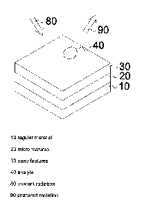
The general schematic diagram of the use of the present sensor is illustrated
in
Figure 3 which shows a number of sensor pads on the substrate surface may
vary from one to a plurality thereof and may not necessarily have a square
section nor all be uniform. More particularly the sensor pad is formed on the
surface of a titanium substrate 10, with micro features 20 formed on the
surface
and nano features 30, specifically nanofibers formed over and around the micro
features. As a sensor an analyte 40 is bound to the sensor pad and incident
radiation 80 is incident on the pad and scattered radiation 90 is detected and
analyzed.
16
CA 02834006 2013-11-19
This approach can be used in analytical scenarios such as volatile organic
compounds (VOCs), in groundwater samples or hydrocarbon mixtures in
petroleum refinery or recovery. The uses of device disclosed herein includes,
but
are not limited to: environmental monitoring, genomics and proteomics
research,
DNA analysis, pharmaceutical industry, drug industry, agriculture and food
analysis, biomedical diagnosis, bio-defence, industrial monitoring, forensic
analysis etc.
Nanofibers
One aspect of this disclosure is the the 3D self-supported nanofiber
structure made from titanium. The nanofibers are composed of generally
spherical NPs that interact in a manner as to arrange themselves into
essentially
single-strand or multi-strand components that form a multiplicity of porous
web-
like features having the capability of supporting themselves in a 3D
architecture.
The interactions and arrangements of the sensor occur usually without chemical
additions or reagents but rather are induced by the laser ablation plasma
dynamics. When submerged into a liquid solution, it is found that the
nanofiber
matrix has some degree of solubility. The titania and fiber matrix is found to
be
partially dissolved, displaced or any combination thereof, in simulated body
fluid
(SBF) solutions. In the SBF solutions, some of the nanofiber matrix remained
underneath the hydroxyapatite precipitation yet some may have been embedded
into the SBF deposits (for example, reference Tavangar et al.). In all of the
cases, the solubility, displacement or combination thereof, properties of the
17
CA 02834006 2013-11-19
nanofiber network suggest that the 3D nanofiber network actively interacts
with
the applied analyte.
In some embodiments, the nano-fibers may be optionally combined with
plasmonic materials to further enhance the optical sensing capabilities. This
combination may be in the form of a film coating, NP coating, alloying,
sintering,
structural combination or any combination thereof.
System Component
In some embodiments, the sensor may be incorporated into a larger
system. For example, the substrate may be incorporated into a micro-electro-
mechanical system (MEMS). MEMS are integrated systems comprising
mechanical elements, sensors, actuators, and electronics. All of those
components may be manufactured by known microfabrication techniques on a
common chip, comprising a silicon-based or equivalent substrate (e.g.
PolyMUMPS). The sensor components of MEMS may be used to measure
mechanical, thermal, biological, chemical, optical, magnetic or any
combination
thereof, phenomena. The electronics may utilize the information from the
sensors
and control actuator components such pumps, valves, lasers, ultrasonic
devices,
magnetic resonance devices, dialysis devices, heaters, coolers, filters, etc.
In some embodiments, the sensor surface may deliver certain
nanostructured material, drugs, hormones, molecular species or a combination
thereof when the sensor is activated. The sensor disclosed herein may act as a
component in a monitoring device that functions as a closed-loop system for
molecular delivery and health monitoring.
18
CA 02834006 2013-11-19
Non-Limiting Example of Nano fiber Sensor Development for Titania
In some embodiments, the broad laser processing parameters to
producing the titania based SERs sensors are as follows: the laser wavelength
may be varied in a range from about 532 to about 1064 nm, the laser pulse
intensity may be varied in a range from about 106 to about 1014 W/cm2, the
pulse
repetition rate may be varied in a range from about 4 to about 26 MHz, the
irradiation time may be varied in a range from about 0.1 to about 25 msec, and
the pulse duration may be varied in a range from about 100 fs to about 10 Ps.
In other embodiments the wavelength may be in a range of the
fundamental modes from about 790 to about 1100 nm and including their second
and third harmonics, and wherein the laser pulse intensity is in a range from
about 106 to about 1014 W/cm2, and wherein the pulse repetition rate is in a
range
from about 1 to 90 MHz, and wherein the effective irradiation time is in a
range
from about 0.1 to about 25 msec, and wherein pulse duration is in a range from
about100 Is to about 10 Ps.
Figure 1 shows a scanning electron microscopy (SEM) image of the 3D
titania nanofibrous network with this particular network shown is generated at
a
wavelength of 1040 nm, repetition rate of 13 MHz and an irradiation time of 20
msec (i.e. from about 13 MHz and 20 msec), pulse intensity of 1.1x10¹³W/cm2,
and a pulse duration of 214 fs. Other variations of laser repetition rate and
irradiation time yield similar SEM images, with variations in nanofibrous
porosity,
3D network depth and the total effect on the substrate (e.g. depth of the
micro-
vias, micro-via rim height etc.).
19
CA 02834006 2013-11-19
Figure 2 is a transmission electron microscopy (TEM) image of the partial
3D titania nanofibrous network that is transferred by electrostatic
interactions to a
TEM grid; the particular network shown is generated with the same parameters
as with Figure 1, except varying the pulse repetition rate and irradiation
time as
well as adding a subsequent irradiation event to increase the distribution of
nanoparticle diameter sizes. The repetition rate and irradiation time were
first set
to 4 MHz and 1 msec respectively and the subsequent irradiation event was set
to 26 MHz and 10 msec respectively. Other variations of laser repetition rate,
irradiation time, and subsequent irradiation processing steps yield similar
TEM
images, with variations in nanofibrous aggregation, individual NP size
distribution, and length of the nanofiber segments.
The nanofibers are typically found to arrange into porous web structures
such as shown in Figure 1. These pores are on average 750 ¨ 850 nm and
increase with a reducing laser pulse repetition rate. When the nanofibers are
partially removed from the 3D network by a TEM grid, the nanofibers tend to
maintain their NP to NP coordination as evidenced from TEM images (Figure 2).
Also witnessed from TEM images is that the individual NPs can have multiple
titania phases. TEM images also reveal that these individual NPs may
sometimes sinter into a single NP or into a nanowire.
The produced nanofibers are found to be generally flexible and mobile.
For example, the nano-fiber matrix is found to be highly elastic over a large
range
of forces with atomic force microscopy (AFM). The nano-fibrous matrix may be
penetrated by the AFM scanning tip in contact mode and it is possible for the
CA 02834006 2013-11-19
scan to continue without significant interference from the AFM probe. Under
dense and thick nano-fiber network conditions, however, significant
interference
during the scan is noticed as the scanning signal saturates and noise
dominates
the image. This is determined to be an effect of variable mechanical
properties of
the 3D nano-fibrous matrix by varying the synthesis parameters.
Referring to the electron microscopy images of titania nano-fibers of
Figures 1 and 2, the individual titania NPs can range in size from several
hundred nm down to several nm. The most average NP size is found to be in the
range of 20-30 nm and increasing with lower laser pulse repetition rates. The
NPs are also essentially spherical when considered individually. The X-ray
diffraction (EDX) patterns indicate that the NPs are generally crystalline.
When
analyzed by EDX at the synthesis parameters at a repetition rate of 13 MHz and
an irradiation time of 20 msec, the 0 atomic weight is determined to be
approximately 74% and the Ti atomic weight is determined to be approximately
26%. Other variations of laser repetition and irradiation time result in
approximately 6% deviations in Ti and 0 atomic weights.
In order to control the NP average diameter and size distribution, the laser
irradiation time may be increased from 1 msec to 10 msec. This may reduce the
average NP size from essentially 90-105 nm to essentially 40-50 nm. As another
example, it may be desirable to reduce the laser pulse repetition rate from 26
MHz to 13 MHz to narrow the NP size distribution or the average size
deviation.
For titania nano fibers, this may reduce the standard deviation by essentially
10
nm. This preceding synthesis control example is universal by material and
varies
21
CA 02834006 2013-11-19
only quantitatively by magnitude. Controlling the nanofiber crystal structure
and
composition may be necessary to further control the analyte dynamics at the
disclosed sensor surface. By reducing the pulse repetition rate from 26 MHz to
4
MHz, a gradual increase in the amount of anatase titania content was observed.
In some optical sensor designs, a greater anatase phase composition may be
more favorable for photocatalytic and surface energy features. Moreover, an
increase in laser irradiation time from about 10 msec to about 25 msec has
been
observed to increase the amount of Ti amorphous content. To reduce the degree
of oxidation, an increase in pulse duration from about 214 fs to the ps regime
may be desirable. A clear indication of reduced titania oxidation is a shift
from a
white colored pigment to a blue colored pigment.
To optimize the 3D nanofibrous titania sensor that can be reproduced by
this disclosure, it may be necessary to adjust the parameters in the following
manner: vary the irradiation time from about 0.1 msec to about 25 msec and
vary
the laser pulse repetition rate from about 4 MHz to about 26 MHz. Naturally,
this
method of varying the combination of laser irradiation time and repetition
rate
may result in an array sensor product (plurality of sensor pads shown in
Figure
3). In terms of the MHz-msec synthesis parameters (i.e. laser pulse repetition
rate and irradiation time), the array sensor may have all, selected or single
combinations in some pattern on the surface. For example, the surface may have
square patches of the nanostructured titania material of a certain dimension
and
certain separations. For synthesized square patches: 1-2 mm was found to be a
minimum separation to reduce nanofiber overlapping, a separation up to 5 mm is
22
CA 02834006 2013-11-19
a minimum to contain the analyte droplet from wetting other adjacent
patches/sensor pads. For individual micro-vias: the separation criteria
depends
on the laser intensity (e.g. repetition rate affecting material heating) and
pulse
duration (e.g. reduced duration reduces the plasma width and increase its
height). As a result, higher intensity and longer pulse duration can
accommodate
larger spacing for nanofibrous network generation. The discovered rule of
thumb
for the range of parameters disclosed herein is to separate the vias by their
diameter.
For the titania 3D nanofibrous optical sensor, the synthesis irradiation time
increment is 5 msec. As well, the preferred pulse repetition rates for the
synthesis of the optical sensor may be 4, 8, 13, and 26 MHz noting that these
are
the equipment limited repetition rates, and any frequency in the range from
about
4 to about 26 MHz will work. Synthesis may be performed under ambient
atmosphere conditions or partial vacuum or conditions between these two.
Figure 4 shows a titanium substrate 10 having a micro surface pattern
110 formed therein by the laser processing discussed above, and a nanowire
web structure 100 formed over and around the micro surface pattern 110. The
micro surface pattern 110 may have features 130 below the sensor base surface
120.
Figure 5 is a diagrammatic representation showing a non-limiting example
of a web structure 100 formed by nanofiber 51. As noted above, the composition
and morphology of the nanofiber depends on the synthesis parameters and
experimental conditions. In the nanofiber some of the nanoparticles (NPs) may
23
CA 02834006 2013-11-19
be rutile NPs 210, and others may be anatase NPs 220, and still others may be
an alloy 240 of rutile and anatase. Some of the NPs in the nanofiber 51 may be
separated by a nanogap 200 but are still aligned with their neighbors by the
weak
forces discussed above. Some of the NPs 260 may be sintered together (i.e.,
being held together by strong forces such that several NPs are sintered to
form a
nanowire. Some of the NPs 280 may be oxidized, coated, contaminated or a
combination thereof. Sections of the nanowire that are branching are shown at
230, and a looped section forming part of the web structure is shown at 270.
The
ability of the nanofiber to stretch and compress in reaction to force is
diagrammatically illustrated by the two nodes 250a and 250b. Nodes 250a and
250b are essentially nodes that stretch apart or approach each other to
provide
an impression of nanofiber stretching/compressing. Such stretching has been
experimentally observed by the inventors.
There may be one or more statistical distributions of the size of the NPs.
For example, considering the NP diameter distribution of about 5 to about 150
nm, there may be a lognormal distribution for NPs on the lower range and
another lognormal distribution for NPs on the higher range. This may be
related
to the presence of two titania phases, e.g. anatase and rutile, but we have
yet to
confirm with certainty (results not published). Simply said, there is a
statistical
distribution of nanofiber NP diameters as opposed to a single diameter chosen
from about 5 to about 150 nm.
Analyte Sensor Examples
24
CA 02834006 2013-11-19
This disclosed procedure of varying the laser pulse repetition rates and
dwell times is used in demonstrating the practicality of using the sensor as a
sensor for bisphenol-A (BPA), diclofenac sodium salt (DCFNa) BPA and DCFNa,
non-limiting examples chosen due to their characterization as common water
pollutants. For BPA, a useful set of laser synthesis parameters for a 3D
titania
nanofibrous optical device is setting the repetition rate and irradiation time
combinations to about 13 MHz and 20 msec respectively (dry residue) and 4
MHz and 1 msec respectively (aqueous) while keeping the laser wavelength at
1040 nm, and pulse duration at 214 fs. For DCFNa, the optimum set of synthesis
parameters for a 3D titania nanofibrous optical sensor is about 8 MHz and 15
msec (dry residue) and no clear optimum for aqueous. By generalizing the
results from BPA and DCFNa, the repetition rate (MHz) and irradiation time
(msec) synthesis parameters with the best analyte detection include
essentially
8-1,8-15,13-15,13-20, and 26-10 (MHz¨msec). Based on average
performance, the 13 MHz and 15 msec synthesis parameter supports the
smallest standard deviation while the 13 MHz and 20 msec synthesis parameter
supports the largest standard deviation of Raman sensor performance.
The G normalized roughness construct described in this disclosure may
be used to test and assure the quality of the synthesized titania sensor. The
array of synthesis parameters range from essentially 4 MHz and 1 msec to
essentially 26 MHz and 25 msec, inclusively as previously described in this
section while keeping the laser wavelength at 1040 nm, and pulse duration at
214 fs. A normalized roughness construct is developed as G = Sa ¨ Sa/Max,
CA 02834006 2013-11-19
where Sa (V) is the average roughness and Max (V) is the maximum roughness.
The G = -0.0021 to +0.0411 criteria is found to correspond to functioning
optical
sensors for BPA and DCFNa. As a result, a device can be analyzed with the
disclosed G criteria to predict the optical sensing performance.
Optionally, it is also found that these nanofibers may be coated with a dye
such as rhodamine 6g (R6G) or crystal violet (CV) to enhance the detection
capability of the analyte. An effective method of coating the nanofiber
network is
found to be first applying a drop of the dye over top of the nanofibrous
network
and subsequently drying the dye with a laser. Effective laser specifications
are
found to include a continuous laser beam in the visible wavelength (e.g. 514
nm),
laser power between 1 mW and 100 mW, laser focus spot size of 5-10 pm and
an irradiation time of up to one minute. The skilled artisan will realize that
the
methods and apparatus are not limiting as to the type of analysis that may be
performed, but rather that the methods and apparatus suggest an effective
method for the detection, identification, quantification or any combination
thereof
of aromatic environmental pollutants such as BPA and DCFNa.
Optical Sensor Method
Incident electromagnetic energy, preferably a visible (VIS) or otherwise an
ultra-violet (UV) or an infrared (IR) laser, is focused onto the sensor. The
power
of the incident energy used to irradiate the analyte is typically below the
analyte's
damage threshold. This threshold may vary from W/cm2 to kW/cm2 depending on
the analyte and the specific experimental conditions. A power density higher
than
the analyte's damage threshold may be desired for applications including but
not
26
CA 02834006 2013-11-19
limited to, analyzing molecular reaction dynamics, catalysis, photo-
initiation, laser
ablation, charge transfer, degradation, physical phase transformation,
crystallographic phase transformation, resin curing, cellular uptake, cellular
damage etc.The generated Raman signal of the analyte, substrate or a
combination thereof, is essentially detected and transmittedto a computer for
the
purposes of analyte detection, identification, quantification or any
combination
thereof. A non-limiting example of a Raman detection unit is disclosed by U.S.
Pat. No. 6,002,471 which is incorporated herein in its entirety by reference.
In another embodiment, a portable version of the Raman spectrometer
may be used. As a non-limiting example, the portable version may be in the
form
of a hand-held device as offered by Ocean Optics, Florida (U.S.). The Raman
system may also use hyperspectral spectrometer principles that can offer
instantaneous spatial information of the sensor surface. In this case, the
acquired
information may be compared immediately between spatially separated points of
interest. As a non-limiting example, theRaman hyperspectral spectrometer may
be in the form provided by P&P Optica, Ontario (Canada) or by Photon etc.,
Quebec (Canada). In the aforementioned embodiments, a variety of laser
wavelengths may be used in sequence or simultaneously during various
experimental stages. Pulsed laser beams, continuous laser beams, or a
combination thereof may be used.
In another embodiment, the optical sensor is readily suitable for other
optical sensor methods known in the art such as normal Raman scattering,
Raman microprobe, confocal Raman microspectrometry, UV-Raman microscopy,
27
CA 02834006 2013-11-19
surface-enhanced Raman scattering (SERS), surface enhanced resonance
Raman spectroscopy (SERRS), tip-enhanced Raman spectroscopy (TERS),
hyper-Raman, coherent anti-Stokes Raman spectroscopy (CARS), stimulated
Raman scattering, inverse Raman spectroscopy, stimulated gain Raman
spectroscopy, three-dimensional Raman, or any combination thereof.
An embodiment of a titanium based Surface Enhance Raman Scattering
(SERS) system comprises a sensor including a titanium substrate having a
surface and an array of sensor locations located in a predefined portion of
the
surface, with each of the sensor locations including a micro-pattern feature
in the
surface of the substrate and nanofibers that generally surround and envelop
the
micro-pattern feature. The nanofibers are comprised of a plurality of titanium
based nanoparticles aligned into a self-supported web structure, with the
array of
sensor locations exhibiting SERS activity. The system includes a sample cell
for
receiving the sensor with the sample cell being configured to allow exposure
of
the sensor to a fluid being tested for the presence of an analyte. A laser
source is
positioned for illuminating the array of sensor locations with laser light and
a
detector is positioned for detecting laser light scattered from the sensor
post
exposure of the sensor to the fluid.
Generally computer control for determining the presence of the analyte
would not be necessary because the user/operator can usually tell the presence
of the analyte by judging the spectrum. However an operator may need
assistance interpreting the spectrum if the spectrum is something new to the
user/operator. Thus, optionally a computer processor may be included which is
28
CA 02834006 2013-11-19
programmed to match the detected spectrum of the scattered light to a spectral
library of analytes.
In some embodiments, the analytes may be partially or fully Raman
labeled. In other embodiments, the nanostructured surface may be Raman
labeled. The Raman labels may be subsequently irradiated to promote curing,
drying, diffusion, mixing, or a combination thereof. The skilled artisan will
realize
that the methods and apparatus are not limiting as to the type of analytes
that
may be detected, identified, quantified or any combination thereof.
Optical Sensor Method Extension to Field Applications
In some embodiments, the sensor surface may be exposed to the analyte
by direct contact with the region of interest. As a non-limiting example, one
may
press the sensor surface against an unknown powder of any orientation and
subsequently use the said sensor for Raman analysis. In another example, the
material may be essentially transparent to the laser beam. In this case, the
sensor surface may be pressed against the unknown powder and the laser beam
may provide excitation for the Raman scattered energy from the backside of the
sensor surface. In essence, the surface would not be relieved from the region
it
contacted and the Raman spectrum may be collected immediately, preferably by
a portable Raman system. A non-limiting example of this portable Raman system
is offered by Ocean Optics, Florida (U.S.).
The said examples for the determination of unknown powders may also be
extended to liquid and gaseous analysis. A non-limiting case includes a
container
with an interior geometry that acts to contain the liquid or gas. The interior
29
CA 02834006 2013-11-19
geometry will have a single or a plurality of developed sensor surfaces. The
container is transparent to the laser beam which may be a form of glass or
quartz. The container is then irradiated by the laser beam from the exterior
to
reach the interior area with the developed sensor surface. Subsequently, the
Raman scattered energy is collected back from the interior and registered by
the
portable Raman system. In case of the container being a vial, such a portable
Raman system is currently offered by Ocean Optics, Florida (U.S.). The
aforementioned portable Raman system extensions are not exclusive to field
applications and may readily be adapted for a laboratory or manufacturing
environment.
As used herein, the terms, "comprises" and "comprising" are to be
construed as being inclusive and open ended, and not exclusive. Specifically,
when used in this specification including claims, the terms, "comprises" and
"comprising" and variations thereof mean the specified features, steps or
components are included. These terms are not to be interpreted to exclude the
presence of other features, steps or components.
The foregoing description of embodiments of the sensor disclosed herein
has been presented to illustrate the principles of the invention and not to
limit the
invention to the particular embodiment illustrated. It is intended that the
scope of
the invention be defined by all of the embodiments encompassed within the
following claims and their equivalents.
CA 02834006 2013-11-19
REFERENCES CITED
Canadian Patent Documents
2566123 May 2005 Poponin
2611985 June 2006 Joseph et al.
U.S. Patent Documents
5580655 December 1996 El-Shall et al.
20050018274 January 2005 Halas et al.
6778316 August 2004 Halas et al.
20050221072 October 2005 Dubrow et al.
20050038498 February 2005 Dubrow et al.
7385691 June 2008 Islam et al.
20030231304 December 2003 Chan et al.
6970239 November 2005 Chan et al.
7400395 July 2008 Chan et al.
6002471 December 1999 Quake
Other References
Musumeci, A. et al., "SERS of Semiconducting Nanoparticles (TiO2 Hybrid
Composites)," J. Am. Chem. Soc. (2009) 131: 6040-6041.
Tan, B. et al., "Synthesis of Fibrous Nanoparticle Aggregates by Femtosecond
Laser Ablation in Air," Opt. Express (2009) 17:1064-1069.
31
CA 02834006 2013-11-19
Jariwala, S. et al., "Micro-Fluidic Channel Fabrication via Two-Photon
Absorption
(TPA) Polymerization Assisted Ablation," J. Micromech. Microeng. (2009) 19:
115023 1-115023_6.
Sivayoganathan, M. et al., "Effect of Mega-Hertz Repetition Rate on the
Agglomerated Particle Size of Femtosecond Synthesized Nanostructures," Opt.
Mater. Express (2012) 2: 987-995.
Maznichenko et al., "TiO2Nanofibrous Interface Development for Raman
Detection of Environmental Pollutants," App. Phys. Lett. (2012) 101: 231602_1-
231602_5.
Tavangar et al., "Synthesis of Bio-Functionalized Three-Dimensional
TitaniaNanofibrous Structures Using Femtosecond Laser Ablation,"
ActaBiomater. (2011) 7: 2726-2732.
32