Note : Les descriptions sont présentées dans la langue officielle dans laquelle elles ont été soumises.
CA 02837756 2013-11-28
WO 2012/167284
PCT/US2012/040811
1
ELECTRO-ACTIVE LENSES INCLUDING THIN GLASS SUBSTRATES
CROSS-REFERENCES TO RELATED APPLICATIONS
[0001] This application claims the benefit of U.S. Serial No. 61/492,433
filed on June 2,
2011; U.S. Serial No. 61/494,637 filed on June 8,2011; and U.S. Serial No.
61/513,708 filed on
August 1, 2011, the contents of which are incorporated by reference in their
entireties.
BACKGROUND OF THE INVENTION
[0002] The present invention relates to electro-active lenses, which may
include, for
example, ophthalmic lenses such as spectacle lenses, and/or non-ophthalmic
lenses, such as a
camera lens, etc. More specifically, the present invention relates electro-
active cells including
one or more thin glass layers, as well as to lenses which may include such
cells.
[0003] Electronic lenses and electronic focusing eyeglasses are known
and now
commercially available. US Patent Nos. 6,619,799; 7,290,875; 6,626,532; and
7,009, 757 (the
contents of which are hereby incorporated by reference herein for all
purposes) are presented as
selective examples of electronic focusing ophthalmic lenses and/or eyeglasses
that teach how an
electronic lens or electronic focusing eyeglasses are made.
[0004] Presently the only electronic focusing eyeglasses commercially
available are retailing
for about $1,250 for a pair which includes the electronic frames, electronic
lenses, charger, and
all coatings. There are two major components that drives up the cost of goods
of such electronic
focusing eyeglasses and both pertain to the cost of the electronic lenses.
Presently the electronic
lenses have to be made out of an expensive 1.67 optical grade plastic called
MR 10 sold by
Mitsui. This is because the index of refraction of the diffractive region and
the liquid crystal
must be closely matched when the electronic lens is turned off. In addition to
a good index match
in the off state, it is important to maintain a relatively small diffractive
height (less than 4
microns ideally). This requires a relatively large average index of the LC
needs, so that the
change in index when the lens is activate is large enough to produce the
desired amount of phase
shift for a relatively thin layer of liquid crystal.
CA 02837756 2013-11-28
WO 2012/167284
PCT/US2012/040811
2
[0005] Because the diffractive region is located on the external front
surface of the 1.67 back
semifinished lens blank, the significant bulk of the material with the present
electronic focusing
lens is made from an expensive premium material. And because the index of the
liquid crystal
must closely match that of the 1.67 back, the material selection which can be
used to make
today's commercially available electronic focusing ophthalmic lens is very
much limited.
[0006] Thus there is a pressing need for an ophthalmic focusing lens
and/or electronic
eyeglasses that allows for a much lower cost of goods and is material
independent. By material
independent it is meant allows for a plurality of different materials which
comprises the bulk the
electronic semi-finished lens blank.
[0007] Other factors to consider include the fact that, while plastic
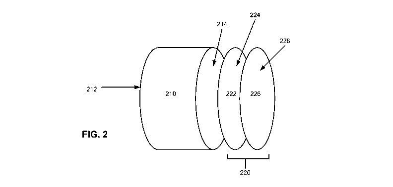
lenses are light weight,
they have tendency to scratch. On the other hand, glass is highly scratch
resistant but is heavy.
Glass-plastic composite lenses have been tried in the past but have tended to
fail due to thermal
expansion differences causing delamination of the glass from the plastic.
[0008] Also, with electronic eyeglasses, the front lid is approximately
1.3mm thick. For
grooved lenses the groove is set at 1.3mm from front thus the groove is
located at the interface of
the front lid optical substrate and the back optical substrate.
[0009] With regard to electronic spectacle lenses there is a need for
improved and novel
ways to create less expensive lens products that meet safety and durability
standards.
BRIEF SUMMARY OF THE INVENTION
[0010] The invention disclosed herein provides a simplified way of
constructing an
electronic focusing ophthalmic lens, which can be materially independent of
the lens blank. One
significant aspect of the invention is that the liquid crystal cell is self
contained, can be stand
alone, and is made independent of the semi-finished lens blank to which it is
later attached or
affixed.
[0011] In addition, the invention disclosed herein provides for a much
reduced cost of goods
compared to today's only commercially available electronic focusing ophthalmic
lens and / or
electronic focusing eyeglasses. The invention disclosed herein provides for an
ophthalmic
focusing lens having material independence.
CA 02837756 2013-11-28
WO 2012/167284
PCT/US2012/040811
3
[0012] According to first aspects of the invention, an electro-active
optical cell is provided
including a layer of electro-active material, a front glass substrate member,
and a back glass
substrate member. In embodiments, the optical cell is capable of independently
providing
changeable optical power with the application of an electrical potential. In
embodiments, the
optical cell is configured to be affixed to an external surface of a
plastic/polycarbonate substrate
and to provide the changeable optical power, with at least one of the front
substrate or the back
substrate of the optical cell being an outermost optical layer (excluding
coatings and other
surface treatments).
[0013] In embodiments, a plurality of differently shaped, or configured,
lens blanks may be
provided for assembling with a standard electro-active optical cell.
[0014] In embodiments, one of the glass substrates may be conformal with
a lens blank
surface and/or one of the glass substrates may be parallel with a diffractive
optic.
[0015] In embodiments, the optical cell may be configured such that
front and rear surfaces
are not parallel. For example, the front of the cell may have less curvature
(i.e. be flatter) than
the back of the cell. Such configurations may be beneficial, for example, in
optimizing the form
of the cell after it is fixed to a lens blank.
[0016] In embodiments, the layer of electro-active material has a
thickness less than
approximately 10[tm. In embodiments, either of the glass substrate members may
have a
thickness between, for example, 20[tm and 1000pm, 20[tm and 500pm, 100[tm and
500pm, or
100[tm and 250pm.
[0017] In embodiments, the cell may be configured to provide no optical
power when the
electrical potential is turned off
[0018] In embodiments, the cell may have at least one of switchable
optical power, tunable
optical power, and changeable optical power, when the electrical potential is
turned on
[0019] In embodiments, the cell may be configured to be affixed to the
front of a lens
comprising fixed optical power. In alternative embodiments, the cell may be
configured to be
affixed to the back of a lens comprising fixed optical power.
CA 02837756 2013-11-28
WO 2012/167284
PCT/US2012/040811
4
[0020] In embodiments, one of the substrate members may be coated on an
outer surface
with a antireflection coating. In embodiments, one of the substrate members
may be coated on
an outer surface with a scratch resistant coating.
[0021] In embodiments, one of the substrate members may be capable of
being surfaced and
polished to create the front or back surface of an optical lens.
[0022] In embodiments, the electro-active material comprises liquid
crystal.
[0023] In embodiments, at least one of the glass substrates may comprise
a surface relief
diffractive surface formed thereon. In embodiments, the electro-active cell
may include a
pixilated region.
[0024] In embodiments, at least one of the glass substrates may comprise a
spherical
curvature.
[0025] According to further aspects of the invention, a method of
manufacturing an electro-
active lens product is provided including providing a first optical layer
having at least one
convex or concave finished surface, and disposing a pre-formed electro-active
optical cell
opposite the at least one convex or concave finished surface such that the
electro-active optical
cell provides at least one of an outer anterior or posterior surface of a
finished lens (not including
coatings or other surface treatments). Such optical cells may include any of
those described
further herein.
[0026] In embodiments, the electro-active optical cell may include a
layer of electro-active
material having a thickness less than 50 [tm, 10[Lm or 5 [tm, an anterior
glass substrate member,
and a posterior glass substrate member, and may be configured to provide a
changeable optical
power.
[0027] According to further aspects of the invention, a lens product is
provided including a
first optical layer including a convex anterior or concave posterior surface;
and an electro-active
cell including a first glass layer, a second glass layer, and a liquid crystal
layer disposed between
the first and second glass layers.
[0028] In embodiments, the first glass layer and the second glass layer
each have a thickness
between 20[tm and 1000pm, 20[tm and 500[Lm, 100[Lm and 500[Lm, or 100[Lm and
250[tm.
CA 02837756 2013-11-28
WO 2012/167284
PCT/US2012/040811
[0029] In embodiments, the first optical layer is a semi-finished lens
blank with an
unfinished posterior or anterior surface.
[0030] In embodiments, the liquid crystal layer has a thickness less
than 50 pm, lOpm or 5
pm.
5 [0031] In embodiments, the second glass layer may have a thickness
between 250 [tm and
500pm.
[0032] In embodiments, the electro-active cell may be configured to
operate as a standalone
cell capable of providing changeable optical power with the application of an
electrical potential.
[0033] In embodiments, at least one of the first glass layer and the
second glass layer may
include a surface relief diffractive surface formed thereon.
[0034] In embodiments, at least one of the first glass layer and the
second glass layer may
include a spherical curvature.
[0035] In embodiments, the lens product may include a diffractive region
and a refractive
region in optical communication with one another. For example, the first
optical layer may
include a refractive region and the electro-active cell may include a
diffractive region in optical
communication with the refractive region.
[0036] Embodiments may include a plastic glass composite lens having a
glass front surface
of a thickness less than 200 microns. In embodiments, the lens may be an
electronic focusing
lens, or a static lens. In embodiments, the lens may be a progressive addition
lens or a single
vision lens.
[0037] Additional features, advantages, and embodiments of the invention
may be set forth
or apparent from consideration of the following detailed description,
drawings, and claims.
Moreover, it is to be understood that both the foregoing summary of the
invention and the
following detailed description are exemplary and intended to provide further
explanation without
limiting the scope of the invention claimed. The detailed description and the
specific examples,
however, indicate only preferred embodiments of the invention. Various changes
and
modifications within the spirit and scope of the invention will become
apparent to those skilled
in the art from this detailed description.
CA 02837756 2013-11-28
WO 2012/167284
PCT/US2012/040811
6
BRIEF DESCRIPTION OF THE DRAWINGS
[0038] Aspects and features of the invention will be understood and
appreciated more fully
from the following detailed description in conjunction with the figures, which
are not to scale, in
which like reference numerals indicate corresponding, analogous or similar
elements.
[0039] Figure 1 shows a cross section of an exemplary electro-active cell
according to first
aspects of the invention.
[0040] Figure 2 shows a lens assembly including an electro-active cell
according to further
aspects of the invention.
[0041] Figure 3 shows another lens assembly including an electro-active
cell according to
further aspects of the invention.
[0042] Figure 4 shows spectacles including lenses with an electro-active
cell according to
further aspects of the invention.
DETAILED DESCRIPTION OF THE INVENTION
[0043] It is understood that the invention is not limited to the
particular methodology,
protocols, and reagents, etc., described herein, as these may vary as the
skilled artisan will
recognize. It is also to be understood that the terminology used herein is
used for the purpose of
describing particular embodiments only, and is not intended to limit the scope
of the invention.
It also is be noted that as used herein and in the appended claims, the
singular forms "a," "an,"
and "the" include the plural reference unless the context clearly dictates
otherwise. Thus, for
example, a reference to "a layer" is a reference to one or more layers and
equivalents thereof
known to those skilled in the art.
[0044] Unless defined otherwise, all technical and scientific terms used
herein have the same
meanings as commonly understood by one of ordinary skill in the art to which
the invention
pertains. The embodiments of the invention and the various features and
advantageous details
thereof are explained more fully with reference to the non-limiting
embodiments and examples
that are described and/or illustrated in the accompanying drawings and
detailed in the following
description. It should be noted that the features illustrated in the drawings
are not necessarily
drawn to scale, and features of one embodiment may be employed with other
embodiments as
the skilled artisan would recognize, even if not explicitly stated herein.
Descriptions of well-
CA 02837756 2013-11-28
WO 2012/167284
PCT/US2012/040811
7
known components and processing techniques may be omitted so as to not
unnecessarily obscure
the embodiments of the invention. The examples used herein are intended merely
to facilitate an
understanding of ways in which the invention may be practiced and to further
enable those of
skill in the art to practice the embodiments of the invention. Accordingly,
the examples and
embodiments herein should not be construed as limiting the scope of the
invention, which is
defined solely by the appended claims and applicable law. Moreover, it is
noted that like
reference numerals reference similar parts throughout the several views of the
drawings.
[0045] The following preferred embodiments may be described in the
context of exemplary
active ophthalmic lens devices for ease of description and understanding.
However, the
invention is not limited to the specifically described devices and methods,
and may be adapted to
various assemblies without departing from the overall scope of the invention.
For example,
devices and related methods including concepts described herein may be used
for other lenses
and optical systems, and other apparatus with electro-active optical elements.
[0046] As used herein, an electro-active element refers to a device with
an optical property
that is alterable by the application of electrical energy. The alterable
optical property may be, for
example, optical power, focal length, diffraction efficiency, depth of field,
optical transmittance,
tinting, opacity, refractive index, chromatic dispersion, or a combination
thereof An electro-
active element may be constructed from two substrates and an electro-active
material disposed
between the two substrates. The substrates may be shaped and sized to ensure
that the electro-
active material is contained within the substrates and cannot leak out. One or
more electrodes
may be disposed on each surface of the substrates that is in contact with the
electro-active
material. The electro-active element may include a power supply operably
connected to a
controller. The controller may be operably connected to the electrodes by way
of electrical
connections to apply one or more voltages to each of the electrodes. When
electrical energy is
applied to the electro-active material by way of the electrodes, the electro-
active material's
optical property may be altered. For example, when electrical energy is
applied to the electro-
active material by way of the electrodes, the electro-active material's index
of refraction may be
altered, thereby changing the optical power of the electro-active element.
[0047] The electro-active element may be embedded within or attached to
a surface of an
ophthalmic lens to form an electro-active lens. Alternatively, the electro-
active element may be
embedded within or attached to a surface of an optic which provides
substantially no optical
CA 02837756 2013-11-28
WO 2012/167284
PCT/US2012/040811
8
power to form an electro-active optic. In such a case, the electro-active
element may be in optical
communication with an ophthalmic lens, but separated or spaced apart from or
not integral with
the ophthalmic lens. The ophthalmic lens may be an optical substrate or a
lens.
[0048] A "lens" is any device or portion of a device that causes light
to converge or diverge
(i. e., a lens is capable of focusing light). A lens may be refractive or
diffractive, or a
combination thereof. A lens may be concave, convex, or planar on one or both
surfaces. A lens
may be spherical, cylindrical, prismatic, or a combination thereof A lens may
be made of
optical glass, plastic, thermoplastic resins, thermoset resins, a composite of
glass and resin, or a
composite of different optical grade resins or plastics. It should be pointed
out that within the
optical industry a device can be referred to as a lens even if it has zero
optical power (known as
plano or no optical power). However, in this case, the lens is usually
referred to as a "plano lens".
A lens may be either conventional or non-conventional. A conventional lens
corrects for
conventional errors of the eye including lower order aberrations such as
myopia, hyperopia,
presbyopia, and regular astigmatism. A non-conventional lens corrects for non-
conventional
errors of the eye including higher order aberrations that can be caused by
ocular layer
irregularities or abnormalities. The lens may be a single focus lens or a
multifocal lens such as a
Progressive Addition Lens or a bifocal or trifocal lens. Contrastingly, an
"optic", as used herein,
has substantially no optical power and is not capable of focusing light
(either by refraction or
diffraction). The term "refractive error" may refer to either conventional or
non-conventional
errors of the eye. It should be noted that redirecting light is not correcting
a refractive error of the
eye. Therefore, redirecting light to a healthy portion of the retina, for
example, is not correcting
a refractive error of the eye.
[0049] The electro-active element may be located in the entire viewing
area of the electro-
active lens or optic or in just a portion thereof. The electro-active element
may be located near
the top, middle or bottom portion of the lens or optic. It should be noted
that the electro-active
element may be capable of focusing light on its own and does not need to be
combined with an
optical substrate or lens.
[0050] The invention disclosed herein relates to various embodiments of
electronic
ophthalmic lenses also referred to as electro-active ophthalmic lenses.
Ophthalmic lens as
defined herein refer to spectacle eyeglass lenses, contact lenses, intraocular
lenses, or any lens
that focuses, transmits, directs, and or refracts light onto the retina of the
user/wearer's eye.
CA 02837756 2013-11-28
WO 2012/167284
PCT/US2012/040811
9
When used as a spectacle lens a tilt switch or similar sensor connected to an
ASIC or micro
controller may cause the spectacle lens to change its optical power.
[0051] Embodiments of the invention may generally include an electro-
active cell which
contains, by way of example only, liquid crystal (which is an electro-active
material). The
electro-active cell is free standing (meaning it is capable of changing
optical power in a
standalone manner) when electricity or an electrical potential is applied. The
electro-active cell
containing liquid crystal is named herein to be that of a liquid crystal cell.
[0052] While the electronic liquid crystal cell can be produced
independently and in large
quantity in most cases it is affixed to the front finished convex lens surface
of a semi-finished
lens blank. It should be pointed out that the liquid crystal cell can be
applied also the back
surface of a semi-finished lens blank when the back concave surface is
finished and whereby the
front convex surface is unfinished.
[0053] In certain other embodiments the liquid crystal cell can be
applied to a non-finished
surface of a non-finished lens blank. It should be pointed out that in all
cases the electro-active
cell has one of its substrate members affixed to a semi-finished lens blank,
or lens and the other
substrate member having an outer front surface that is exposed to air (not
taking into account any
coatings or treatments to its front surface etc.)
[0054] According to first aspects of the invention, an electro-active
optical cell is provided,
such as illustrated in Figure 1. As can be seen in Figure 1, an electro-active
cell 100 may include
a layer of electro-active material 150 (e.g. liquid crystal or electro-chromic
material), a first glass
substrate member 110, and a second glass substrate member 120. A seal 160 may
be disposed
around the electro-active material 150, and may be formed, for example, from
either of first glass
substrate member 110, or second glass substrate member 120, or from an
independent spacer
material inserted between the substrates.
[0055] In embodiments, the layer of the electro-active material 150 has a
thickness less than
approximately lOpm, or less than approximately 5[Lm. In embodiments, either of
the glass
substrate members 110, 120 may have a thickness between, for example, 20[tm
and 1000pm,
20[tm and 500[Lm, 100[tm and 500[Lm, or 100[Lm and 250[tm. Thicker substrates
may be used,
CA 02837756 2013-11-28
WO 2012/167284
PCT/US2012/040811
for example, to allow for a particular front, or back, substrate to be
surfaced and/or polished as
the outer surface of a finished lens.
[0056] Electro-active cell 100 may also include layers 130, 140 which
may include, for
example, electrodes and/or alignment layers for influencing/activating the
electro-active material
5 150. The electrodes may be a layer of ITO located on each substrate.
These two layers of ITO
form the electrodes needed to provide the electrical potential to switch,
change, or tune the
optical power of the liquid crystal lens cell. Typically, in the absence of an
electric field between
the electrodes, the liquid crystal molecules align in the same direction as
the alignment direction.
In the presence of an electric field between the electrodes, the liquid
crystal molecules orient in
10 the direction of the electric field. In an electro-active element, the
electric field is perpendicular
to the alignment layer. Thus, if the electric field is strong enough, the
orientation of the liquid
crystal molecules will be perpendicular to the alignment direction. If the
electric field is not
strong enough, the orientation of the liquid crystal molecules will be in a
direction somewhere
between the alignment direction and perpendicular to the alignment direction.
[0057] Either of layers 130, 140 may include, for example, pixilated
electrodes, or other
patterned electrodes for influencing and/or activating discreet portions of
the electro-active
material 150. In embodiments, the cell 100 may be configured to provide no
optical power when
the electrical potential is turned off. In embodiments, the cell 100 may have
at least one of
switchable optical power, tunable optical power, and changeable optical power,
when the
electrical potential is turned on.
[0058] Either of the outer surfaces of first glass substrate member 110
or second glass
substrate member 120 may be configured to joining with a lens blank. Likewise,
either of the
outer surfaces of first glass substrate member 110 or second glass substrate
member 120 may be
configured to be surfaced and polished to create the front or back surface of
an optical lens.
[0059] Electro-active cell 100 may be configured to be capable of
independently providing
changeable optical power with the application of an electrical potential. In
embodiments, the
electro-active cell 100 is configured to be affixed to an external surface of
a
plastic/polycarbonate substrate and to provide the changeable optical power,
with at least one of
the first substrate 110 or the second substrate 120 being an outermost optical
layer (excluding
coatings and other surface treatments).
CA 02837756 2013-11-28
WO 2012/167284
PCT/US2012/040811
11
[0060] In embodiments, electro-active cell 100 may be configured such
that its front and rear
surfaces are not parallel. For example, the front of the cell (e.g. first
substrate110) may have less
curvature (i.e. be flatter) than the back of the cell (e.g. second substrate
120). Such
configurations may be beneficial, for example, in optimizing the form of the
cell after it is fixed
to a lens blank.
[0061] In embodiments, one of the substrate members 110, 120 may include
diffractive
element (e.g. a surface relief diffractive) on a front or back surface thereof
In embodiments, one
of the substrate members 110, 120 may include a spherical curvature. In
embodiments, one of
the substrate members 110, 120 may be coated on an outer surface with a
antireflection coating.
In embodiments, one of the substrate members 110, 120 may be coated on an
outer surface with
a scratch resistant coating.
[0062] In a preferred embodiment of the invention the electronic liquid
cell is affixed to the
front convex surface of the semi-finished lens blank while the back unfinished
surface of said
semifinished lens blank is finished by way of surfacing and polishing and / or
free forming or
digital surfacing. In a preferred embodiment the liquid crystal cell is formed
by way of a front
substrate of glass member having a thickness ranging between 250 microns and
500 microns and
a back substrate member of glass having a thickness which ranges between 250
microns and 500
microns.
[0063] In embodiments, one of the two glass substrates members may have
a surface relief
diffractive surface formed thereon and the other glass substrate member may be
spherical in
curvature. The formation of the surface relief diffractive on the glass
surface can be by way of
etching. In a preferred embodiment, the surface relief diffractive may be
formed on the front
convex surface of the back glass substrate member.
[0064] However in another preferred embodiment, the surface relief
diffractive may be
formed on the back concave surface of the front glass substrate member. A thin
layer (e.g. less
than 10 microns) of liquid crystal is deposited and located on the top surface
of the surface relief
diffractive surface. In some cases this layer of liquid crystal may be, for
example, less than 5
microns thick.
CA 02837756 2013-11-28
WO 2012/167284
PCT/US2012/040811
12
[0065] The glass substrate member having a diffractive surface area
located thereon is
comprised of an index of refraction which matches closely that of the liquid
crystal when the
electronic liquid crystal cell is turned off. An alignment layer is typically
formed on the surface
of the diffractive after it is coated with ITO. However, it should be noted
that the alignment
layer can be formed on the surface of the diffractive and the ITO can be
deposited over the
alignment layer.
[0066] The index of refraction of the opposite glass spherical substrate
member can be that
of any index of refraction.
[0067] In certain embodiments, an adhesive, which in most cases, but not
all, is index
matched to that of the refractive index of the liquid crystal when the liquid
crystal cell is turned
off (or the electronic focusing lens is turned off) and is applied such that
the two glass substrates
members become affixed to one another thus encapsulating the liquid crystal in
between.
[0068] In other embodiments of the invention, the front glass substrate
member and the back
glass substrate member, after being coated with ITO and then Si02, are bonded
by way of laser
fusion or anodic bonding. And in an additional embodiment of the invention,
the front glass
substrate member and the back glass substrate member, after being coated with
ITO, are bonded
by way of laser fusion or anodic bonding. In this additional embodiment of the
invention,Si02 is
not used even though laser fusion and anodic bonding are utilized to secure
the front glass
substrate member to the back glass substrate member of the liquid crystal
cell. For clarity, a
liquid crystal cell is a type of electro-active cell.
[0069] As mentioned previously, a significant aspect of the invention is
that the liquid crystal
cell is self contained (can be stand alone) and is made independently of that
of the semi-finished
lens blank to which it is attached or affixed. This allows for the liquid
crystal cell to be made in
quantity and separately which allows for improved manufacturing efficiency and
cost reduction.
Further is should be understood that once the liquid crystal cell is affixed
or attached to the semi-
finished lens blank it is then known as an electronic semi-finished lens
blank. And once the
electronic semifinished lens blank is finished by way of surfacing and
polishing, and / or free
forming or digital surfacing the electronic lens blank is then known as an
electronic focusing lens
blank. Finally once the electronic focusing lens blank is edged or shaped into
that of a lens
capable of being mounted into an eyeglass frame it is known as an electronic
focusing lens.
CA 02837756 2013-11-28
WO 2012/167284
PCT/US2012/040811
13
[0070] Given that the liquid crystal cell of the inventive ophthalmic
electronic lens is self
contained and works in a standalone manner it allows for being affixed to any
optical grade
plastic material and even glass. This allows for the inventive electronic lens
as taught herein to
utilize much less expensive optical grade materials that become the bulk of
the electronic semi-
finished lens blank; such as polycarbonate or even CR39, both of which are
inexpensive optical
grade materials for making ophthalmic lenses or eyeglasses.
[0071] In some embodiments, but not all, the liquid crystal cell has no
optical power when
electricity or the electrical potential is not applied or is removed. And has
optical power when
electricity or the electrical potential is applied. In these embodiments the
two glass substrate
members are parallel to one another and neither comprises any optical power.
In certain
embodiments the two parallel glass substrate members are curved to match the
front convex
curvature of the plastic semi-finished lens blank.
[0072] In other embodiments the two parallel glass substrate members are
curved to match
the back concave curvature of the plastic semi-finished lens blank. In certain
other embodiments
(which are not fail safe) the liquid crystal cell has optical power when
electricity or the electrical
potential is not applied or is removed, and has no optical power when
electricity or the electrical
potential is applied.
[0073] As used herein, the term dynamic means the optic is capable of
changeable optical
power as opposed to being a fixed static optical power. The add power region
is the region of
the electronic lens that dynamically increases plus optical power over and
beyond the distance
optical power. This change can be in steps of optical power or by way of
continuous optical
power.
[0074] As shown in Figure 2, an exemplary embodiment of the invention
may include a
semi-finished lens blank 210, which may be, for example, an MR8 plastic, or
other
polycarbonate or plastic material.
[0075] A back surface 212 of the lens blank 210 may be unfinished, and a
front surface 214
of the lens blank 210 may be shaped to a convex shape, suitable for joining
with the back surface
of an electro-active cell as described herein. The lens blank 210 may be
manufactured in
different sizes and/or material compositions to provide for a range of
potential optical power.
CA 02837756 2013-11-28
WO 2012/167284
PCT/US2012/040811
14
Thus, a plurality of differently shaped, or configured, lens blanks may be
provided for
assembling with a standard electro-active optical cell.
[0076] As also shown in Figure 2, an electro-active cell 220 may include
a back substrate
member 222 with a front convex surface 224, and a front substrate member 226
with a convex
front surface 228. The back surface of substrate member 222 may be concave and
configured to
join together, substantially conformally, with the front surface 214 of the
lens blank 210. In such
configurations, the front surface of the electro-active cell 220, e.g. the
front surface of front
substrate member 226, may be capable of being surfaced and polished to create
the front surface
of an optical lens. It should be noted that the electro-active cell 220 may
include similar features
and/or functionality to the cell 100 shown in Figure 1, unless otherwise
specified.
[0077] The electro-active cell 220 also includes a liquid crystal
material (not shown) between
the back and front substrate members, and, in embodiments, may also include
one or more
electrode and alignment layers, as well as a diffractive element.
[0078] In embodiments, the layer of the electro-active material may have
a thickness less
than approximately 10um, or less than approximately Sum. In embodiments,
either of the
substrate members 222, 226 may have a thickness between, for example, 20um and
1000um,
20um and 500um, 100um and 500um, or 100um and 250um.
[0079] In embodiments, the electro-active cell 220 may be pre-fabricated
and form a stand-
alone unit, which can be assembled to various lens blanks at the point of
sale, or other locations.
Other embodiments will also be described with reference to Figure 2.
[0080] In embodiments, both of back substrate member 222 and front
substrate member 226
may be made of glass. The front convex surface 224 of back substrate member
222 may include
a diffractive element and/or a seal to contain the liquid crystal material.
The use of two glass
substrates has a number of advantages which may include, material independence
of the
substrates for the electro-active cell, globally accepted materials, reduced
overall material and
processing costs, allow for high-temperature processing, inherent scratch
resistance, no need for
metal molds. This allows for making an electronic focusing lens cell that is
very thin; e.g. 150 -
200 microns thin. This is because the front and back substrates may be made
with ¨75 - 100
micron glass. The front and back substrates, with all internal layers, can be
bonded together by
CA 02837756 2013-11-28
WO 2012/167284
PCT/US2012/040811
way of, for example, adhesive, laser bonding, or melting. Such glass
substrates may also flex to
that of the lens blank curve, thus solving the problem of thermal expansion
and contraction.
[0081] In embodiments, the convex front surface 228 of the front
substrate member 226 may
be spherical.
5 [0082] In embodiments, the order of the components shown in Figure
2 may be reversed.
That is, the electro-active cell 220 may be configured to be joined to the
back of a lens blank. In
such circumstances, the electro-active cell 220 may join, for example, to a
concave back surface
of lens blank 210, and the back surface of the electro-active cell 220 may be
exposed to air. In
such configurations, the back surface of the electro-active cell 220 may
include a substrate that is
10 capable of being surfaced and polished to create the back surface of an
optical lens.
[0083] Yet another alternative embodiment is depicted in Figure 3. As
shown in Figure 3,
embodiments may include a semi-finished lens blank 310, which may be, for
example, an MR8
plastic, or other polycarbonate or plastic material.. A back surface 312 of
the lens blank 310 may
be unfinished, and a front surface 314 of the lens blank 310 may be shaped to
a convex shape,
15 suitable for joining with the back surface of an electro-active cell as
described herein. The lens
blank 310 may be manufactured in different sizes and/or material compositions
to provide for a
range of potential optical power. In such configurations, the front surface of
the electro-active
cell 320, e.g. the front surface of substrate member 326, may be capable of
being surfaced and
polished to create the front surface of an optical lens.
[0084] As also shown in Figure 3, an electro-active cell 320 may include a
front substrate
member 326 with a convex front surface 328. The back surface of substrate
member 326 may be
formed with a cavity for receiving the electro active material and various
other elements of the
electro-active cell, such as electrode and alignment layers, as well as a
diffractive element. It
should be noted that the electro-active cell 320 may include similar features
and/or functionality
to the cell 100 shown in Figure 1, unless otherwise specified.
[0085] The electro-active cell 320 also includes a liquid crystal
material (not shown) behind
the front substrate member 326, and, in embodiments, may also include one or
more electrode
and alignment layers, as well as a diffractive element.
CA 02837756 2013-11-28
WO 2012/167284
PCT/US2012/040811
16
[0086] In embodiments, the layer of the electro-active material may have
a thickness less
than approximately lOpm, or less than approximately 5pm. In embodiments, the
substrate
member 326 may have a thickness between, for example, 20[tm and 1000pm, 20[tm
and 500[Lm,
100[Lm and 500[Lm, or 100[Lm and 250[tm.
[0087] In embodiments, the electro-active cell 320 may be pre-fabricated
and form a stand-
alone unit, which can be assembled to various lens blanks at the point of
sale, or other locations.
Other embodiments will also be described with reference to Figure 3.
[0088] In embodiments, the front substrate member 326 may be made of
glass. The front
substrate member 326 may include a back concave surface 329 which may include
a diffractive
element and/or a seal to contain the liquid crystal material.
[0089] In embodiments, the convex front surface 328 of the front
substrate member 326 may
be spherical.
[0090] In embodiments, the order of the components shown in Figure 3 may
be reversed.
That is, the electro-active cell 320 may be configured to be joined to the
back of a lens blank. In
such circumstances, the electro-active cell 320 may join, for example, to a
concave back surface
of lens blank 310, and the back surface of the electro-active cell 320 may
include the substrate
326 exposed to air. In such configurations, the back surface of the electro-
active cell 320 may
include a substrate that is capable of being surfaced and polished to create
the back surface of an
optical lens.
[0091] As noted above, electro-active elements and/or cells as described
herein may include
individually addressable regions (e.g. "pixels") that may allow for selective
activation of sub-
regions of the electro-active material. Thus, spectacle lenses according to
aspects of the
invention can also provide for advanced control and tracking, such as
responding to the eye
translating across the spectacle lens, and controlling the lens based on the
location of the pupil of
the wearer's eye, e.g. to activate a particular progressive region etc.
[0092] In embodiments, the entire electro-active cell may be configured
to turn on and off at
the same time. In other cases, portions of the electro-active cell, when
individually addressed,
may be tuned to turn on or off at different times from one another. When such
a design is used,
CA 02837756 2013-11-28
WO 2012/167284
PCT/US2012/040811
17
an eye tracking system may be used to control such functions. For example, the
pupil of the
wearer's eye may be tracked to selectively activate regions of the electro-
active material.
[0093] The diameter of each individually addressable region may be, for
example, within at
least about 0.25 ium2 . In certain cases, the electro-active material and/or
corresponding
electrodes may cover the majority of the electro-active cell and optical
surface of the ophthalmic
host lens that is within optical communication with the pupil of the eye of
the wearer. In other
embodiments, the electro-active material and/or corresponding electrodes may
cover less than
the majority of the electro-active cell and optical surface of the ophthalmic
host lens that is in
optical communication with the pupil of the eye of the wearer. This could be,
for example, for
the use of the invention with certain types of spectacle lenses and/or gaming
or entertainment
spectacles or eyewear.
[0094] The electro-active optical region can be of a structure that is
pixilated or surface relief
diffractive. When pixilated it can be individually addressed, when surface
relief diffractive one
common set (top and bottom) of electrodes can be used. The optical power can
be made to be
different if desired by way of the electrode design for when pixilated or the
surface relief
diffractive pattern. The optical design of a diffractive optical surface
capable of providing plus
optical power is known in the trade. It should be pointed out that when the
index of refraction of
the liquid crystal found within the optical power region is equal to that of
the substrate on which
it is located the optical power is mostly zero and the diffractive optical
power region
substantially disappears.
[0095] The optical power of each optical power region when activated can
be within the
range of +0.50D to +4.00D and most preferably within the range of +1.00D to
+3.00D. If the
electrical potential is applied such that it is not affecting all refractive
optical power regions at
the same time or of the same magnitude this would be accomplished by way of
multiple
insulated electrodes located on one or both substrates that are individually
addressed.
[0096] These refractive regions can be designed, by way of example only,
by way of
structure of refractive curves or a Fresnel optical design. The optical design
of a refractive
optical surface capable of providing plus optical power is known in the trade.
It should be
pointed out that when the index of refraction of the liquid crystal found
within the optical power
CA 02837756 2013-11-28
WO 2012/167284
PCT/US2012/040811
18
region is equal to that of the substrate on which it is located the optical
power is mostly zero and
the refractive optical power region substantially disappears.
[0097] It should be pointed out that all measurements, dimensions,
optical powers, shapes,
figures, illustrations, provided herein by way of example and are not intended
to be self limiting.
[0098] The liquid crystalline material discussed herein may be a nematic
liquid crystal, a
twisted nematic liquid crystal, a super-twisted nematic liquid crystal, a
cholesteric liquid crystal,
a smectic bi-stable liquid crystal, or any other type of liquid crystalline
material. An alignment
layer is a thin film, which, by way of example only, may be less than 100
nanometers thick and
constructed from a polyimide material. The thin film is applied to the surface
of substrates that
comes into direct contact with liquid crystalline material. Prior to assembly
of the electro-active
element, the thin film is typically buffed in one direction (the alignment
direction) with a cloth
such as velvet. When the liquid crystal molecules come in contact with the
buffed polyimide
layer, the liquid crystal molecules preferentially lie in the plane of the
substrate and are aligned
in the direction in which the polyimide layer was rubbed (i.e., parallel to
the surface of the
substrate). Alternatively, the alignment layer may be constructed of a
photosensitive material,
which when exposed to linearly polarized 1N light, yields the same result as
when a buffed
alignment layer is used.
[0099] To reduce power consumption, a bi-stable liquid crystalline
material may be used. A
bistable liquid crystalline material may switch between one of two stable
states with the
application of electrical power (with one state being an activated state and
the other state being a
deactivated state). The bi-stable liquid crystalline material remains in the
one stable state until
sufficient electrical power is applied to switch the bi-stable liquid
crystalline material to the other
stable state. Thus, electrical power is only needed to switch from one state
to the other and not
to remain in a state. The bi-stable liquid crystalline material may switch to
a first state when +5
volts or more is applied between the electrodes and may switch to a second
state when -5 volts or
less is applied between the electrodes. Of course other voltages, both higher
and lower, are
possible.
[00100] The liquid crystal may alter its refractive index over the visible
spectrum by at least
0.1 units upon electrical activation. As used herein, the "visible spectrum"
refers to light having
a wavelength in the range of about 400 ¨ 750 nm. A liquid crystal (LC) layer
may include a
CA 02837756 2013-11-28
WO 2012/167284
PCT/US2012/040811
19
guest-host mixture capable of altering the optical transmission of light upon
electrical activation.
As used herein, the optical transmission of a layer or device refers to the
percentage of light
energy that is transmitted through the layer or device and not lost to
absorption or scattering.
Preferably, the mixture is capable of altering the optical transmission by at
least about 30% -
99% upon activation. The liquid crystal layer may be pixilated as previously
described, and may
be electrically addressable in discrete portions of at least about 0.25 ium2
without affecting the
response of adjacent portions. The liquid crystal layer may be controllable by
a computerized
device, such as a processor and associated software, which may be capable of
arbitrarily
addressing multiple segments in a preprogrammed or adaptable manner. The
software may be
permanently embodied in a computer-readable medium, such as a special-purpose
chip or a
general purpose chip that has been configured for a specific use, or it may be
provided by a
digital signal. The software may be incorporated into a digital signal
processing unit embedded
into a vision correcting device.
[00101] In embodiments, such as where the electro-active cell is intended to
provide a
darkening or tinting function, the electro-active material may include a layer
of liquid crystal
doped with a dye material such as a dichroic dye. By doping the liquid crystal
molecules with
the dye material, the dye molecules align themselves with the liquid crystal
molecules. The dye
molecules are polar and rotate to align with an applied electrical field. The
optical absorption of
the dye material depends on the orientation of the individual dye molecules
with respect to an
incident optical wave. In a deactivated state with homogeneous (horizontal)
alignment of the
liquid crystal molecules, when the electric field between the electrodes is
not strong enough, the
dye molecules align with the alignment layers and the absorption of light
through the liquid
crystal is minimized or maximized, depending upon the relative orientation
between the dipole
moment and the direction of orientation of the dye molecule. In an activated
state with
homogeneous (horizontal) alignment of the liquid crystal molecules, when the
electric field
between the electrodes is strong enough, the dye molecules rotate and align
with the orientation
of the electric field, perpendicular to the alignment direction. In this
orientation, the absorption
of light though the liquid crystal is minimized. The opposite may be the case
when a
homeotropic (vertical) alignment of the liquid crystal is used such that
absorption is minimized
in a deactivated state and maximized in an activated state. A ferroelectric
liquid crystalline
material may also be used.
CA 02837756 2013-11-28
WO 2012/167284
PCT/US2012/040811
[00102] According to embodiments of the invention, two electrodes made of
transparent
electrodes by way of example only, such as indium tin oxide, may be provided.
One electrode
may be found on the inside layer of each substrate. It should be pointed out
this invention also
contemplates one electrode being located on the innermost surface of one
substrate and the
5 outermost surface of the second substrate or both electrodes being
located on the outermost
surface of both substrates.
[00103] A self contained sealed electronics module may be provided in various
of the
embodiments, and may comprise two substrates, two electrodes, coatings, and
liquid crystal.
Once the appropriate coatings, and electrodes are deposited on the common
optical surfaces of
10 the two substrates, the two substrates may then be affixed to one
another by way of example
only, an adhesive and / or glass laser fusion. The substrates may be
hermetically sealed after the
two substrates are affixed together and have the appropriate electronics
applied for making the
electro-active cell fully functional. Such a stand-alone optical unit can also
be called a self
contained sealed electronics module.
15 [00104] Assembled lenses, including an electro-active cell as described
herein, may be used in
spectacles, such as shown in Figure 4. A spectacle system 400 may included
electro-active cells
410 attached to lens blanks. The spectacles 400 may also include sensor(s) 420
and a
controller/power source 430.
[00105] Various exemplary lenses may include embedded sensors, such as sensor
420 shown
20 in Figure 4. The sensor may be, for example, a range finder for
detecting a distance to which a
user is trying to focus. The sensor may be light-sensitive cell for detecting
light that is ambient
and/or incident to the lens or optic. The sensor may include, for example, one
or more of the
following devices: a photo-detector, a photovoltaic or UV sensitive photo
cell, a tilt switch, a
light sensor, a passive range-finding device, a time-of-flight range finding
device, an eye tracker,
a view detector which detects where a user may be viewing, an accelerometer, a
proximity
switch, a physical switch, a manual override control, a capacitive switch
which switches when a
user touches the nose bridge of a pair of spectacles, a pupil diameter
detector, or the like. The
sensor may also include one or more micro electro mechanical system (MEMS)
gyroscopes
adapted for detecting a tilt of the user's head or encyclorotation of the
user's eye.
CA 02837756 2013-11-28
WO 2012/167284
PCT/US2012/040811
21
[00106] The sensor may be operably connected to a lens controller, such as
controller 430
shown in Figure 4. The sensor may detect sensory information and send a signal
to the controller
which triggers the activation and/or deactivation of one or more dynamic
components of the lens
or optic.
[00107] The sensor, by way of example only, may detect the distance to which
one is
focusing. The sensor may include two or more photo-detector arrays with a
focusing lens placed
over each array. Each focusing lens may have a focal length appropriate for a
specific distance
from the user's eye. For example, three photo-detector arrays may be used, the
first one having a
focusing lens that properly focuses for near distance, the second one having a
focusing lens that
properly focuses for intermediate distance, and the third one having a
focusing lens that properly
focuses for far distance. A sum of differences algorithm may be used to
determine which array
has the highest contrast ratio (and thus provides the best focus). The array
with the highest
contrast ratio may thus be used to determine the distance from a user to an
object the user is
focusing on.
[00108] Some configurations may allow for the sensor and/or controller to be
overridden by a
manually operated remote switch. The remote switch may send a signal by means
of wireless
communication, acoustic communication, vibration communication, or light
communication
such as, by way of example only, infrared. By way of example only, should the
sensor sense a
dark room, such as a restaurant having dim lighting, the controller may cause
changes to the lens
that impact the user's ability to perform near distance tasks, such as reading
a menu. The user
could remotely control the lens or optic to increase the depth of field and
enhance the user's
ability to read the menu. When the near distance task has completed, the user
may remotely
allow the sensor and controller to act automatically thereby allowing the user
to see best in the
dim restaurant with regard to non-near distance tasks.
[00109] When the inventive embodiment is that of a spectacle lens the sensing
is that of, by
way of example only, a range finder, micro-accelerometer, tilt switch, micro-
gyroscope,
capacitor touch / swipe switch. Any one or all of these sensors can be built
into the inventive
ophthalmic host lens or that of the eyeglass frame that houses the inventive
dynamic spectacle
lens.
CA 02837756 2013-11-28
WO 2012/167284
PCT/US2012/040811
22
[00110] Lenses may also include controller connections for connecting the
electro-active cell
to an external power source or controller, a battery, a controller, and/or a
power management
system. Such components may be disposed completely, or partly, within a
peripheral region of
the lens, e.g. 412 in Figure 4.
connections and may be capable of generating an electric field between the
electrodes by
applying one or more voltages to each electrode. In some configurations, the
power module may
be part of the electro-active cell, or the lens blank. The module may be
located outside the
electro-active cell and connect to the electrodes using electrical contact
points in the electro-
[00112] In embodiments, a surface of the electro-active cell may be configured
in a
substantially planar shape. In such configurations, the lens may be configured
to include
refractive index matching between the liquid crystal material included in the
cell and the lens
blank. This can be matched in the activated or inactivated state. In the index
matched state, the
[00113] While illustrative and presently preferred embodiments of the
invention have been
described in detail herein, it is to be understood that the inventive concepts
may be otherwise
variously embodied and employed, and that the appended claims are intended to
be construed to
include such variations, except as limited by the prior art.