Note : Les descriptions sont présentées dans la langue officielle dans laquelle elles ont été soumises.
CA 02838880 2013-12-10
WO 2012/167834
PCT/EP2011/059646
1
A COMPENSATING SYSTEM FOR MEDIUM OR HIGH VOLTAGE APPLICATIONS
TECHNICAL FIELD
The present disclosure relates to a compensating system for a
power system, and in particular to a wye-connected
compensating system.
BACKGROUND
A power system, such as an electric grid, typically comprises
a transmission network which transfers power from power
generating stations, e.g. power plants, and a distribution
network connected to the transmission network for distribution
of the power to loads, such as households and factories
connected to the distribution network.
The transmission network is typically based on a Flexible
Alternating Current Transmission System (FACTS) and/or a High
Voltage Direct Current (HVDC) system.
AC power transmission gives rise to electromagnetic fields
resulting in reactive power components in the grid e.g. due to
inductive and capacitive loads and the inductance of the power
lines.
By decreasing the reactive power, the active power which acts
to operate loads connected to the power system, can be
increased. At other times, it may be desirable to provide
additional reactive power to the power system in order to
stabilize it.
FACTS provide stabilization of a power system by means of
reactive power compensating devices such as Static VAR units
and STATCOM units.
CA 02838880 2013-12-10
WO 2012/167834
PCT/EP2011/059646
2
Static VAR units such as Thyristor Controlled reactors (TCR)
produce harmonics of the fundamental frequency in the power
system. Harmonics are undesired by-products resulting from
switching the thyristors. It is normally desirable to reduce
the harmonic content produced by a TCR. Especially, it is
desirable to prevent or at least reduce the harmonic content
generated by a wye-connected TCR to be fed into the power
system. Compared to a delta-connected TCR, the 3rd, 9th,
= = = , (3n) th harmonic content generated by a wye-connected TCR is
fed into the power system, whilst for a delta-connected TCR
the 3rdf 9th, = = = f (3n) th harmonic current is essentially trapped
as a circulating current in the delta-connection.
STATCOM units utilize voltage converters comprising chain-
linked, i.e. series connected, converter cells having
switchable semiconductor devices. By switching the
semiconductor devices properly in the converter cells, the
amount of reactive power in the grid can be controlled.
Some converter topologies utilise a DC-capacitor in each
converter cell, e.g. H-bridge cells, in order to control the
voltage generated by each converter cell. The DC voltage over
each capacitor should typically be kept constant according to
a respective set-point value both during normal operation of
the power system and under asymmetrical conditions.
For delta-connected STATCOM units, a circulating current is
trapped in the delta-connection, enabling voltage control of
the DC-capacitors in the converter cells. However, for wye-
connected STATCOM units, the current of the STATCOM may be
zero. Voltage control of the DC-capacitors is lost under such
conditions. Therefore, in order to control the voltage level
of the DC capacitors, a current has to be generated and fed to
the DC-capacitors. This current is fed into the power system.
CA 02838880 2013-12-10
WO 2012/167834
PCT/EP2011/059646
3
SUMMARY
A general object of the present disclosure is to provide a
wye-connected compensating system which reduces the harmonic
content fed into the power system to which the compensating
system is connected.
Another object is to provide voltage control of DC-capacitors
of converter cells of a wye-connected compensating system also
at low current operation.
Hence, in a first aspect of the present disclosure there is
provided a compensating system for a power system, wherein the
compensating system comprises: a compensator comprising
semiconductor switch means, which compensator has phase legs
which on a first side of the compensator defines AC inputs for
connection to a respective phase of the power system, wherein
the phase legs are connected in wye connection at a second
side of the compensator, which wye connection has a neutral
point; and a filter arrangement which at a first side thereof
is connected to the neutral point of the wye connection and at
a second side is connected to the AC inputs to thereby form a
circuit with the compensator; wherein the filter arrangement
is arranged such that the circuit acts essentially as an open
circuit for positive sequence currents or voltages and
negative sequence currents or voltages, and as a closed
circuit for zero-sequence currents, wherein the filter
arrangement is further arranged to block a zero-sequence
current having a fundamental frequency and to allow a harmonic
of the zero-sequence current to pass therethrough, whereby the
harmonic of the zero-sequence current is able to flow through
the closed circuit.
The power system is preferably a medium power system or a high
power system.
CA 02838880 2013-12-10
WO 2012/167834
PCT/EP2011/059646
4
Hence a zero-sequence current can be fed through the closed
circuit because of the path provided by the filter arrangement
for zero-sequence currents, thereby allowing a harmonic of the
zero-sequence current to pass through the filter arrangement
and flow through the closed circuit. Hence the harmonic
current will not be fed into the power system. As a result
unwanted harmonics can be reduced in the power system.
The filter arrangement may be arranged to allow a third
harmonic of the zero-sequence current to pass through the
filter arrangement. Thereby a current with a harmonic having a
frequency substantially different than the fundamental
frequency of the power system can flow through the closed
circuit. As a result, the risk that the semiconductor switch
means commence switch operations is reduced, as the
semiconductor switch means are arranged such that they
commence switching based on the fundamental frequency whereby
e.g. reactive effect compensation can be provided during
normal operation of the power system.
The filter arrangement may comprise a band-pass filter which
allows the harmonic to pass therethrough. Thereby only the
desired harmonic is allowed to pass through the filter
arrangement.
The filter arrangement may comprise a zig-zag transformer and
a capacitor in series connection with the zig-zag transformer.
A zig-zag transformer has very high impedance for positive and
negative sequence currents, essentially acting as an open
circuit. Furthermore, a zig-zag transformer allows at least a
portion of a zero-sequence current to pass therethrough.
Hence, the zig-zag transformer provides for one realization of
at least a portion of the filter arrangement. The capacitor
provides filtering e.g. of the fundamental frequency of the
zero-sequence current. Hence, the capacitance of the capacitor
CA 02838880 2013-12-10
WO 2012/167834
PCT/EP2011/059646
should generally be selected such that the filtering
arrangement blocks the fundamental frequency and allows a
harmonic, such as the third harmonic, to pass therethrough.
The filter arrangement may comprise a reactor in series
5 connection with the zig-zag transformer and the capacitor.
As an alternative to the zig-zag transformer, the filter
arrangement may comprise a transformer which on its primary
side is connected to the AC inputs via a wye connection which
provides a transformer neutral point, which transformer
neutral point is in electrical connection with the neutral
point of the compensator. Hence, a regular transformer which
is not a zig-zag transformer may be utilised in order to
provide the filter effect as described above.
The filter arrangement may comprise a capacitor connected in
series with the transformer, the capacitor being arranged
between the transformer neutral point and the neutral point of
the compensator.
The filter arrangement may comprise a reactor connected in
series with the transformer. The reactor may provide a correct
impedance of the filter arrangement if the impedance of the
transformer or zig-zag transformer is too low.
The compensator may be a thyristor controlled reactor, wherein
each semiconductor switch means is a thyristor.
Each phase leg may have a plurality of cell converters
connected in series and each cell converter comprises a DC
capacitor. Thereby the DC capacitor voltage may be controlled
also at conditions of low current when in prior solutions the
voltage of the DC capacitor would not be controllable as
essentially no current would flow through the cell converters.
CA 02838880 2013-12-10
WO 2012/167834
PCT/EP2011/059646
6
Beneficially, by being able to control the DC voltage level of
the individual DC capacitors in the cell converters, wye-
connected voltage source converters such as STATCOM may be
provided. For a wye-connected STATCOM, or other similar cell
converter-based compensating device, fewer chain-linked e.g.
series-connected cell converters can be used than for delta-
connected STATCOM. In particular, the required number of cell
converters for a wye-connected STATCOM is the square root of
the integer three less than for delta-connected STATCOM.
Hence, fewer semiconductor switching means, e.g. IGBT are
required, resulting in substantial cost reductions of the
compensating system. To this end it is to be noted that
generally each cell converter comprises a plurality of series
connected IGBTs in order to be able to handle the high
voltages utilised in high voltage power systems. Hereto, the
filter arrangement is generally of substantially lower cost
than the additional cell converters used in a delta-coupled
STATCOM.
One embodiment may comprise means for controlling the voltage
of each DC capacitor via the harmonic of the zero-sequence
current when flowing in the closed circuit.
Each semiconductor switch means may be an Insulated-Gate
Bipolar Transistor (IGBT).
The compensator may be a STATCOM.
Additional features and advantages will be disclosed in the
following.
BRIEF DESCRIPTION OF THE DRAWINGS
The invention and the advantages thereof will now be described
by way of non-limiting examples, with reference to the
accompanying drawings of which:
CA 02838880 2013-12-10
WO 2012/167834
PCT/EP2011/059646
7
Fig. 1 schematically shows a generic topology of the
compensating system according to the present disclosure.
Fig. 2 shows a schematic circuit diagram of a first example of
a compensating system.
Fig. 3 shows a schematic circuit diagram of a second example
of a compensating system.
DETAILED DESCRIPTION
In the following description, for purpose of explanation and
not limitation, specific details are set forth, such as
particular techniques and applications in order to provide a
thorough understanding of the present disclosure. However, it
will be apparent for a person skilled in the art that the
present disclosure may be practiced in other embodiments that
depart from these specific details. In other instances,
detailed description of well-known methods and apparatuses are
omitted so as not to obscure the description with unnecessary
details.
While in the following positive and negative sequence time
varying electric signals will be referred to as positive and
negative sequence currents, it is to be understood that in all
cases the terms positive and negative sequence voltages,
respectively, are equally valid. Thus, the positive and
negative sequences can be either voltages or currents.
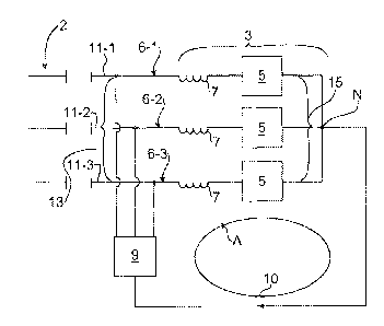
Fig. 1 shows a generic circuit diagram of a compensating
system 1 according to the present disclosure. The compensating
system 1 comprises a compensator 3 having a phase leg 6-1, 6-
2, 6-3 for each electric phase 11-1, 11-2, 11-3. The
compensating system 1 further comprises a semiconductor unit 5
and optionally a reactor 7 at each phase leg 6-1, 6-2, 6-3.
Each semiconductor unit 5 comprises semiconductor switch
CA 02838880 2013-12-10
WO 2012/167834
PCT/EP2011/059646
8
means. The compensator 3 has a first side 13 which defines AC
inputs and which is connectable to an AC network of a high
voltage power system 2. The compensator 3 has a second side 15
at which the phase legs 6-1, 6-2, 6-3 are connected in a wye-
connection. The wye-connection has a neutral point N which is
the point to which each phase leg 6-1, 6-2, 6-3 is connected.
The neutral point N is not grounded in the examples provided
herein.
The compensating system 1 comprises a filter arrangement 9
which on a first side thereof is connected to the neutral
point N of the wye-connection of the compensator 3. The first
side is a side which functions as an input for receiving an
electric parameter such as a current from the neutral point N
of the compensator 3. The filter arrangement 9 has a second
side which is connected to the first side of the compensator
3. The second side of the filter arrangement 9 functions as an
output of the filter arrangement 9 and provides a filtered
electric parameter having been received at the first side of
the filter arrangement 9.
The filter arrangement 9 together with the phase legs 6-1, 6-
2, 6-3 of the compensator 3 defines a circuit 10 for each
phase leg 6-1, 6-2, 6-3. The circuit 10 for the phase leg 6-3
is shown by means of arrow A. It is to be understood that
corresponding circuits can be defined for the remaining phase
legs 6-1 and 6-2.
The filter arrangement 9 is arranged such that the circuit 10
for each phase leg 6 essentially acts as an open circuit for
positive sequence currents and negative sequence currents, and
as a closed circuit for zero-sequence currents.
A positive sequence current is a three-phase current where
each phase is separated by a 120 degree phase angle. The first
CA 02838880 2013-12-10
WO 2012/167834
PCT/EP2011/059646
9
phase has a phase angle defined to be 0 degrees, the second
phase has a phase angle of 120 degrees with respect to the
first phase, and the third phase has a phase angle of 240
degrees with respect to the first phase angle.
A negative sequence current also has a 120 degree phase angle
between the three phases, but in a different order than for
positive sequence currents. Positive and negative sequence
currents are typical in a power system which is subject to
symmetrical conditions, e.g. when each phase is subjected to a
load providing the same impedance for each electric phase.
A zero-sequence current has essentially no phase angle between
the electric phases. Zero-sequence currents may be formed for
instance during asymmetrical conditions, e.g. faults, in the
power system.
The filter arrangement 9 is furthermore arranged to block or
filter the fundamental frequency and most of the harmonics of
the zero-sequence current. The fundamental frequency is herein
defined as the frequency of the voltage or current in the
power system to which the compensating system 1 is connected.
The fundamental frequency is typically 50 or 60 Hz. In
particular, it is preferable that the filter arrangement 9 is
tuned such that one harmonic is allowed to pass through the
filter arrangement 9.
In one embodiment, the harmonic is the third harmonic of the
zero-sequence current, which third harmonic has a frequency
far removed from the fundamental frequency of the zero-
sequence current. The fundamental frequency is utilised for
providing switching of the semiconductor switch means.
Furthermore, the third harmonic has sufficient magnitude for
controlling the voltage level of DC capacitors of the
CA 02838880 2015-08-04
semiconductor units in specific examples of the disclosure, as
will be elaborated in more detail herebelow.
Fig. 2 shows a first example of a compensating system 1-1. The
compensating system 1-1 generally has the same structure as
5 the compensating system 1, except that the semiconductor units
5 in this particular example are cell converters 5-1
comprising semiconductor switch means 4 such as IGBTs.
10 Each phase leg 6 has a plurality of cell converters 5-1
connected in series thereby forming chain-linked cell
converters. The chain-linked cell converters 5-1 of a phase
define a semiconductor unit 5 in Fig. 1.
Each cell converter 5-1 is controlled by a control unit (not
shown). The compensating system 1-1 may have an individual
control unit for each cell converter, or alternatively there
may be a central control unit which provides individual
control signals to each cell converter for one phase leg.
Alternatively the central control unit may be arranged to
provide individual control signals to each cell converter for
all phase legs. The control unit may be arranged to switch the
semiconductor switch means 4 by means of a control signal
based on a reference signal and the AC voltage provided by the
power system 2 when the compensating system 1-1 is connected
thereto.
Each cell converter 5-1 further comprises a DC capacitor 8 for
controlling the voltage level of the output from the cell
converter. Each DC capacitor voltage should preferably be kept
at a set-point value such that the compensator 3-1 can provide
power compensation to the power system 2 when needed. In
particular, the compensator 3-1 should generally always be in
CA 02838880 2013-12-10
WO 2012/167834
PCT/EP2011/059646
11
a state where it is able to provide instantaneous compensation
to the power system 2. By being able to control the DC voltage
level of the DC capacitors also during e.g. asymmetric
conditions, the wye-connected compensator 3 is able to provide
compensation to the power system 2 essentially at any time.
The compensating system 1-1 may also comprise means for
controlling the voltage of the DC capacitors via the zero-
sequence current, based on a respective set-point value.
The filter arrangement 9-1 comprises a zig-zag transformer 9-2
and a capacitor C connected in series with the zig-zag
transformer 9-2. Optionally, the filter arrangement 9-1
comprises a reactor L which is series connected with the
capacitor C. The properties of the zig-zag transformer 9-2
allows the circuit 10 for each phase leg 6-1, 6-2, 6-3 to
essentially act as an open circuit for positive sequence
currents and negative sequence currents, and as a closed
circuit for zero-sequence currents.
As an alternative to the zig-zag transformer 9-2, a
transformer such as regular power transformer may be utilised
in the filter arrangement. In this case, the primary windings
of the transformer are wye-connected with the phase legs of
the compensator at the first side of the compensator.
Furthermore, a neutral point, in the following termed a
transformer neutral point, of the wye-connected primary side
of the transformer is connected in series with a capacitor and
optionally also with a reactor L. The capacitor is connected
to the neutral point N of the wye-connected second side of the
compensator. The secondary side of the transformer is delta
connected. The secondary winding of the secondary side can for
example feed auxiliary power supply for the compensator.
CA 02838880 2013-12-10
WO 2012/167834
PCT/EP2011/059646
12
The capacitor C together with the impedance of the zig-zag
transformer, or as in the above-described variation, the
impedance of the transformer, defines a filter arranged to
block the fundamental frequency of the zero-sequence current.
In one variation, the filter is a band-pass filter arranged to
only allow the one harmonic, such as the third harmonic, of
the zero-sequence current to pass therethrough.
By providing the filter arrangement 9-2, a zero-sequence
current io is able to flow through the closed circuit for each
phase leg 6-1, 6-2 and 6-3. The voltage level of the DC
capacitors 8 may thereby be controlled such that the DC
voltage levels of the DC capacitors 8 correspond to their set-
point values when there is no current supply to the phase legs
6-1, 6-2, 6-3 from the power system 2. Beneficially, when
compensation is needed in the power system 2, the compensator
3 will be able to provide essentially instantaneous power
compensation because the DC capacitors 8 have voltage levels
corresponding essentially to their set-point values.
When the power system 2 is in a normal operational state,
providing e.g. positive sequence currents, the impedance of
the zig-zag transformer 9-2 will be very high and essentially
act as an open circuit. Hence, in this case no current will
flow in the circuit 10.
In a preferred embodiment, the compensator 3-1 is a STATCOM.
It is to be noted that the structure of the cell converters is
not limited to the structure of Fig. 2. Indeed, the cell
converters can have any topology utilised in e.g. STATCOM
units.
Fig. 3 shows a second example of a compensating system 1-2.
The compensating system 1-2 generally has the same structure
as the compensating system 1, except that the semiconductor
CA 02838880 2015-08-04
13
units 5 in the second example for each phase leg 6-1, 6-2, 6-3
are anti-parallel coupled thyristors 14, and that each phase
leg 6-1, 6-2, 6-3 comprises an additional reactor 12. In
particular, the compensator 3-2 is a thyristor controlled
reactor (TCR).
The thyristors 14 are controllable by a control unit (not
shown). The compensating system 1-2 may have an individual
control unit for each thyristor 14, or alternatively there may
be a central control unit which provides individual control
signals to each thyristor 14 for one phase leg. Alternatively
the central control unit may be arranged to provide individual
control signals to each thyristor 14 for all phase legs. The
control unit may thereby be arranged to switch the thyristors
14 by means of a control signal based on a reference signal
and the AC voltage provided by the power system 2.
The filter arrangement 9-2 is the same filter arrangement as
described with reference to Fig. 2, and can hence either
comprise a regular transformer or a zig-zag transformer, as
has been elaborated hereabove.
The compensating system 1-3 provides for a TCR which traps 3r-L
9th,
r (3n)th harmonics which are generated due to switching
of the thyristors 14. In particular, the harmonic content is
trapped in the circuit 10 for each phase leg 6-1, 6-2, 6-3.
The present disclosure enables wye-connection of a compensator
such as a static VAR compensator or a STATCOM, and may be
utilised for high voltage applications in an electric grid.
The scope of the claims should not be limited by the preferred
embodiments set forth in the examples, but should be given the
broadest interpretation consistent with the description as a
whole.