Note : Les descriptions sont présentées dans la langue officielle dans laquelle elles ont été soumises.
CA 02840059 2013-12-19
DESCRIPTION
THERMOELECTRIC CONVERSION ELEMENT AND THERMOELECTRIC
CONVERSION POWER GENERATION DEVICE
TECHNICAL FIELD
[0001]
The present invention relates to a thermoelectric conversion
element and a thermoelectric conversion power generation device.
BACKGROUND ART
[0002]
Thermoelectric conversion elements are known as clean energy
conversion elements without the use of petroleum or ozone, and have been
desired to be made more efficient, larger in area and thinner in recent
years. For example, power generation elements using the Seebeck effect
(thermoelectric conversion power generation elements) and cooling/heating
elements using the Peltier effect (Peltier elements) have been under
development.
[0003]
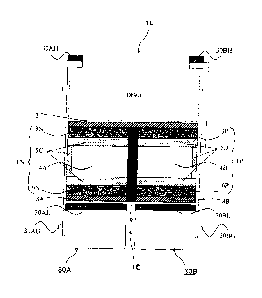
The structure and the principle of such thermoelectric conversion
elements will be described. FIG.
17 is a conception diagram for
illustrating a structure of a conventional thermoelectric conversion
element.
As illustrated in FIG. 17, a conventional thermoelectric conversion
element 100 is composed of a plurality of opposed electrodes (metallic
electrode) 120 and 121, and 180; and a block 130 made of an n-type
thermoelectric semiconductor and a block 131 made of a p-type
1
CA 02840059 2013-12-19
thermoelectric semiconductor which are disposed between the electrodes.
The blocks 130 and 131 are electrically connected with each other by the
electrode 180 at their ends on one side (connection ends). The n-type
thermoelectric semiconductor block and the p-type thermoelectric
semiconductor block are connected in series. The blocks 130 and 131 are
connected to the electrodes 120 and 121, respectively, at their ends on the
other side.
[0004]
In this configuration, thermal energy is converted into electric
energy due to the Seebeck effect by using the electrode 180 as a high
temperature side and the opposite electrodes 120 and 121 as a low
temperature side to create a temperature difference therebetween.
Electric energy is converted into thermal energy also by the Peltier effect
by applying a direct voltage between the electrode 180 and the electrodes
120 and 121 and passing an electric current through the electrode 120 to
the electrode 121 via the electrode 180 so that the electrode 180 acts as an
endothermic electrode, and the electrodes 120 and 121 act as radiative
electrodes, for example.
[0005]
Here, the endothermic energy in the case where the conventional
thermoelectric conversion element is used as a Peltier element will be
discussed. The endothermic energy Q on an upper side of the electrode
180 is represented by the following equation (1):
Q = QP - QR - QK (1),
wherein Qp is an amount of Peltier endotherm, QR is an amount of Joule
heat, and QK is an amount of heat conduction (see FIG. 17).
In addition, specifically, where the height of the blocks (distance
2
CA 02840059 2013-12-19
between the electrode 180 and the electrodes 120 and 121) is L, and the
cross sectional area of the blocks (cross sectional area of a surface
perpendicular to a direction of the height) is S, QR is in proportion to the
height L of the blocks and in inverse proportion to the cross sectional area
S. Furthermore, QK is in proportion to the cross sectional area S of the
blocks and in inverse proportion to the height L. To discuss the shape of
the thermoelectric element, the larger the cross sectional area S is, the
smaller QR is and the larger QK is, provided that the height L of the blocks
is determined, for example. That is, once properties of the material are
determined, the relationship between the cross sectional area S and the
height L will be definitely determined as the shape of the element that
provides ideal thermoelectric conversion efficiency.
[0006]
Using a Bi-Te material as a thermoelectric material, for example,
the thermoelectric conversion element can perform efficient thermoelectric
conversion when the relationship of S (m2) = (0.6 to 6) x 10-3 x L (m) is
satisfied, wherein S (m2) is the cross sectional area of the blocks (in the
shape of a rectangular parallelepiped or a circular cylinder) made of a
Bi-Te material and L (m) is the height thereof. In this case, given a 10 cm
x 10 cm square liquid crystal display panel is cooled with two blocks made
of n-type and p-type thermoelectric semiconductors, for example, the
height L of the blocks of the thermoelectric conversion element needs to be
80 cm or higher, making the thermoelectric conversion element
impracticable. To solve the problem, a plurality of blocks having a cross
sectional area S of approximately 0.01 cm2 to 3 cm2 are connected in
series and modularized, and a thermoelectric conversion element (Peltier
element) enlarged in endotherm area (cooling area) by the modularization
3
CA 02840059 2013-12-19
has been put to practical use.
[0007]
However, the radiating side of the thermoelectric conversion
element reaches a high temperature and the material thereof expands,
whereas the endothermic side reaches a lower temperature and contracts.
Accordingly, in the case of a thermoelectric conversion element in which
the electrodes are adhered to the blocks by soldering, for example, the
adhered region may have fatigue crack due to stress. The larger the area
of the thermoelectric conversion element is, the more significant this
tendency is, and therefore the cooling area of a commercialized Peltier
module is approximately 5 cm x 5 cm.
[0008]
Based on such a background, a technique to inhibit cracking in
the adhered region has been reported. For example, there has been
developed a thermoelectric conversion element module including opposed
carbon substrates, and a plurality of n-type semiconductors and a
plurality of p-type semiconductors planarly arranged between the
substrates, wherein the carbon substrates are formed of a high thermal
conductivity carbon composite material (see Patent Document I, for
example).
According to the patent document, the thermoelectric
conversion element module has superior thermal conductivity to those
including substrates formed of general carbon materials, and can lessen
heat loss in the substrates and prevent cracking in the adhered region
between the substrates and the semiconductors. However, this invention
employs thermoelectric conversion elements having a conventional element
structure, and therefore the thermoelectric conversion elements do not
have sufficient properties. In
addition, the invention employs a
4
CA 02840059 2013-12-19
conventional module structure obtained by modularizing a large number of
thermoelectric conversion elements, and therefore the elements cannot be
sufficiently enlarged in area.
[0009]
In order to improve the efficiency of a thermoelectric conversion
element, there have been reported various techniques to inhibit the
thermal conduction between the endothermic side and the radiating side.
For example, there has been developed a thermoelectric conversion module
including a plurality of pairs of thermoelectric conversion elements each
obtained by linearly arranging a p-type thermoelectric conversion material
and a n-type thermoelectric conversion material, wherein a boundary
between the p-type thermoelectric conversion material and the n-type
thermoelectric conversion material is placed in contact with a high
temperature heat source, and an electric and thermal insulator is placed
on a side of the thermoelectric conversion element for thermally insulating
low temperature parts distal to the boundary from the high temperature
heat source (see Patent Document 2, for example). In this structure,
however, the p-type thermoelectric conversion material and the n-type
thermoelectric conversion material are arranged linearly and continuous
with each other, and thus the thermal conduction between the
thermoelectric conversion materials is not inhibited, and the
thermoelectric conversion elements do not have sufficient properties. In
addition, the module structure is conventional, and therefore the
thermoelectric conversion elements cannot be sufficiently enlarged in area.
[0010]
Furthermore, it has been reported to use a carbon material formed
by conjugating graphene or fullerene and carbon nanotube as a
5
CA 02840059 2013-12-19
thermoelectric conversion material (see Patent Documents 3 and 4, for
example). By conjugating graphene or fullerene and carbon nanotube, it
is possible to reduce the thermal conductivity of the carbon nanotube and
form a thermoelectric conversion material having high electric conductivity.
Consequently, there have been proposed thermoelectric conversion
elements in which these carbon materials are used as thermoelectric
conversion materials. Basically, however, carbon materials do not have
high thermoelectric force, and therefore it is difficult to obtain sufficient
performance from a thermoelectric conversion element formed by merely
improving carbon materials and using the materials as thermoelectric
conversion materials. Accordingly, a large number of thermoelectric
conversion elements need to be modularized, and with such a structure, it
is difficult to enlarge the elements in area.
RELATED ART DOCUMENTS
PATENT DOCUMENTS
[0011]
Patent Document 1: Japanese Unexamined Patent Publication No.
2009-141079
Patent Document 2: Japanese Unexamined Patent Publication No.
HEI 8(1996)-335722
Patent Document 3: Japanese Unexamined Patent Publication No.
2010-192780
Patent Document 4: Japanese Unexamined Patent Publication No.
2010-147379
SUMMARY OF THE INVENTION
PROBLEMS TO BE SOLVED BY THE INVENTION
[0012]
6
CA 02840059 2013-12-19
During the operation of a general thermoelectric conversion
element, heat: QK is conducted from a high temperature effect part (or heat
generation effect part) to a low temperature effect part (or endothermic
effect part) because of the temperature difference: AT between the high
temperature effect part (or heat generation effect part) and the low
temperature effect part (or endothermic effect part). Accordingly, the
thermoelectric conversion element is reduced in thermoelectric conversion
efficiency as the AT decreases.
[0013]
A conventional way to reduce the amount of heat: QK to be
conducted from the high temperature effect part (or heat generation effect
part) to the low temperature effect part (or endothermic effect part) is to
decrease the cross sectional area of a thermoelectric conversion material
layer and increase the thickness of a thermoelectric conversion material
layer. In order to achieve a large area with a thermoelectric conversion
element whose thermoelectric conversion material layer has a decreased
cross sectional area, however, a large number of thermoelectric conversion
elements need to be modularized for use. However, the size of a
thermoelectric conversion module obtained by such modularization is
approximately 5 cm x 5 cm, being incapable of providing a large area.
[0014]
In addition, a conventional thermoelectric conversion element has
a structure in which a high temperature part and a low temperature part
having almost the same area are stacked one on top the other. In the
thermoelectric conversion element having such a structure, an electrode
on the high temperature side and an electrode on the low temperature side
face each other and have a short distance therebetween, and thus the
7
CA 02840059 2013-12-19
thermal conduction from the electrode on the high temperature side to the
electrode on the low temperature side is greater. With such a structure,
therefore, it is difficult to produce a thermoelectric conversion element
having high thermoelectric conversion efficiency. Where the temperature
difference is no more than 10 C in a space at normal temperature, the
thermal energy conducted from the electrode on the high temperature side
to the electrode on the low temperature side is stored in the electrode on
the low temperature, and soon the high temperature side and the low
temperature side will no longer have a temperature difference. At present,
therefore, it is impossible to perform power generation by thermoelectric
conversion using the temperature difference in a space at normal
temperature.
[0015]
Since thermoelectric conversion elements need to satisfy three
sorts of properties: high thermoelectric force, high electric conductivity
and low thermal conductivity at the same time, conventional
thermoelectric conversion elements have been developed by imparting the
three sorts of properties to their materials. However, materials satisfying
the three sorts of properties at the same time are quite limited, and
therefore it is difficult to develop a thermoelectric conversion element
having excellent properties by imparting all the three sorts of properties to
its materials.
[0016]
In view of the above-described circumstances, the present
invention has been made to achieve a structure of a thermoelectric
conversion element capable of satisfying high electric conductivity and low
thermal conductivity at the same time by forming a charge transport layer
8
CA 02840059 2013-12-19
in the element. The present invention is to provide a thermoelectric
conversion element having much higher thermoelectric conversion
efficiency than conventional thermoelectric conversion elements.
Moreover, the present invention is to provide a thermoelectric conversion
element and a thermoelectric conversion power generation device which
can be enlarged in area and which can generate power in a space at
normal temperature.
MEANS FOR SOLVING THE PROBLEMS
[0017]
The present invention provides a thermoelectric conversion
element comprising a thermoelectric conversion section and electrodes,
wherein the thermoelectric conversion section includes at least: a
thermoelectric conversion material section or a thermoelectric conversion
material layer which is formed of a thermoelectric conversion material; and
a charge transport section or a charge transport layer which is formed of a
charge transport material having at least both semiconducting electric
conduction properties and metallic electric conduction properties.
The present invention also provides a thermoelectric conversion
power generation device comprising at least a thermoelectric conversion
power generation element and a Peltier element which are combined with
each other, wherein the Peltier element absorbs heat of a low temperature
effect part of the thermoelectric conversion power generation element and
releases heat to a high temperature effect part of the thermoelectric
conversion power generation element or to an object serving as a heat
reservoir in contact with the high temperature effect part, and the
thermoelectric conversion power generation element generates electric
power.
9
In a broad aspect, moreover, the present invention provides:
(1) A thermoelectric conversion element comprising a thermoelectric
conversion section and electrodes, wherein the thermoelectric conversion
section has one thermoelectric conversion property of either an n-type or
a p-type and includes a thermoelectric conversion material layer and a
charge transport layer, wherein the thermoelectric conversion material
layer is formed of thermoelectric conversion material having
semiconducting electric conduction properties, wherein the charge
transport layer is formed of charge transport material having
semiconducting electric conduction properties so that an ohmic contact is
formed between the thermoelectric conversion material and the charge
transport material, and negligible energy is released or absorbed as charge
carriers in a conduction band of the thermoelectric conversion material
transfer to the conduction band of the charge transport material, and
wherein the charge transport layer is an anisotropic conductive material
layer having anisotropy with respect to conductivity, and the anisotropic
conductive material layer has a larger electric conductivity in a plane
direction than in a thickness direction and charge carriers transported to
the charge transport layer can move in a plane direction of the charge
transport layer.
(2) The thermoelectric conversion element according to (1), wherein
the charge transport material is selected from the group of graphite,
crystalline graphite and graphene, electron transport material and hole
transport material.
9a
CA 2840059 2019-08-19
(3) The thermoelectric conversion element according to (1), wherein
the thermoelectric conversion section includes a laminate structure of at
least the thermoelectric conversion material layer and the charge transport
layer, wherein the charge transport layer comprises extended portions
protruded from the laminate structure, and wherein one of the electrodes
is disposed on the extended portion so that charge carriers can move in a
plane direction of the charge transport layer between the electrode and the
thermoelectric conversion material layer.
(4) The thermoelectric conversion element according to (1), wherein
the thermoelectric conversion section includes a laminate structure in
which at least: a lower thermoelectric conversion material layer, a lower
charge transport layer, an upper charge transport layer and an upper
thermoelectric conversion material layer are laminated in sequence,
wherein the lower charge transport layer and the upper charge transport
layer of the thermoelectric conversion section are spaced by a distance and
continuous with each other along a side surface of the thermoelectric
conversion section and form one charge transport layer, and wherein the
lower thermoelectric conversion material layer and the upper
thermoelectric conversion material layer have the same property of either
.. an n-type or a p-type.
(5) The thermoelectric conversion element according to (1), wherein
the thermoelectric conversion section includes a laminate structure in
which at least: a lower thermoelectric conversion material layer, a lower
9b
CA 2840059 2019-08-19
charge transport layer, a heat insulating layer, an upper charge transport
layer and an upper thermoelectric conversion material layer are laminated
in sequence, wherein the lower charge transport layer and the upper
charge transport layer are continuous with each other along a side surface
of the heat insulating layer and form one charge transport layer, and
wherein the lower thermoelectric conversion material layer and the upper
thermoelectric conversion material layer have the same property of either
an n-type or a p-type.
(6) The thermoelectric conversion element according to (1), wherein
the thermoelectric conversion section includes a laminate structure in
which at least: a lower thermoelectric conversion material layer, a heat
insulating layer and an upper thermoelectric conversion material layer are
laminated in sequence, wherein the heat insulating layer is made of a heat
insulating material including through holes or a porous material and the
through holes or pores of the porous material are provided with a charge
transport material which can form at least a charge transport layer inside
the through holes or the pores, and wherein the lower thermoelectric
conversion material layer and the upper thermoelectric conversion
material layer have the same property of either an n-type or a p-type.
(7) The thermoelectric conversion element according to (1), the
thermoelectric conversion section includes two thermoelectric conversion
material layers and a charge transport layer, wherein one of the two
thermoelectric conversion material layers is disposed on the one end of the
charge transport layer and the other of the two thermoelectric conversion
9c
CA 2840059 2019-08-19
material layers is disposed on the other end of the charge transport layer
so that charge carriers can move in a plane direction of the charge
transport layer between the two thermoelectric conversion material layers,
and wherein the two thermoelectric conversion material layers have the
same thermoelectric conversion property of either an n-type or a p-type.
9d
CA 2840059 2019-08-19
CA 02840059 2013-12-19
EFFECTS OF THE INVENTION
[0018]
The present invention has achieved a structure of a thermoelectric
conversion element capable of satisfying high electric conductivity and low
thermal conductivity at the same time by forming a charge transport
section or a charge transport layer in the element. Accordingly, an effect
of the present invention is that the thermoelectric conversion materials
that are used for the thermoelectric conversion element of the present
invention only need to have high thermoelectric force. In addition, the
present invention provides a thermoelectric conversion element having
much higher thermoelectric conversion efficiency than conventional
thermoelectric conversion elements. Using the thermoelectric conversion
element of the present invention, it is possible to provide a thermoelectric
conversion element and a thermoelectric conversion power generation
device which can be enlarged in area and which can generate power in a
space at normal temperature.
BRIEF DESCRIPTION OF THE DRAWINGS
[0019]
FIG. 1 is a top view, a sectional view and a bottom view of a
thermoelectric conversion element according to Embodiment 1 of the
present invention.
FIG. 2 is a top view, a sectional view and a bottom view of a
thermoelectric conversion element according to Embodiment 2 of the
present invention.
FIG. 3 is a top view, a sectional view and a bottom view of a
thermoelectric conversion element according to Embodiment 3 of the
present invention.
CA 02840059 2013-12-19
FIG. 4 is a top view, a sectional view and a bottom view of a
thermoelectric conversion element according to Embodiment 4 of the
present invention.
FIG. 5 is a top view, a sectional view and a bottom view of a
thermoelectric conversion element according to Embodiment 5 of the
present invention.
FIG. 6 is a top view, a sectional view and a bottom view of a
thermoelectric conversion element according to Embodiment 6 of the
present invention.
FIG. 7 is a top view, a sectional view and a bottom view of a
thermoelectric conversion element according to Embodiment 7 of the
present invention.
FIG. 8 is a top view, a sectional view and a bottom view of a
thermoelectric conversion element according to Embodiment 8 of the
present invention.
FIG. 9 is a top view, a sectional view and a bottom view of a
thermoelectric conversion element according to Embodiment 9 of the
present invention.
FIG. 10 is a sectional view of a thermoelectric conversion power
generation device (device including a plurality of thermoelectric conversion
elements) according to Embodiment 10 of the present invention.
FIG. 11 is a sectional view of a thermoelectric conversion power
generation device (device including a plurality of thermoelectric conversion
elements) according to Embodiment 11 of the present invention.
FIG. 12 is a sectional view of a thermoelectric conversion power
generation device (device including a plurality of thermoelectric conversion
elements) according to Embodiment 12 of the present invention.
11
CA 02840059 2013-12-19
FIG. 13 is a sectional view of a thermoelectric conversion power
generation device (device including a plurality of thermoelectric conversion
elements) according to Embodiment 13 of the present invention.
FIG. 14 is a perspective view for illustrating a structure of a
thermoelectric conversion element (Peltier element) applied to the
thermoelectric conversion power generation device according to
Embodiment 10 of the present invention.
FIG. 15 is a perspective view for illustrating a structure of a
thermoelectric conversion element (Peltier element) applied to the
thermoelectric conversion power generation device according to
Embodiment 12 of the present invention.
FIG. 16 is a top view, a sectional view and a bottom view of a
conventional thermoelectric conversion element according to Comparative
Embodiment 1 of the present invention.
FIG. 17 is a conception diagram for illustrating a structure of the
conventional thermoelectric conversion element.
MODE FOR CARRYING OUT THE INVENTION
[0020]
In general, a thermoelectric conversion element has a structure
having electrodes arranged on and beneath a thermoelectric conversion
material, and one of the electrodes absorbs heat and the other electrode
generates heat when a direct voltage is applied between the electrodes and
a current flows through the thermoelectric conversion material. For
example, the upper electrode absorbs heat and in turn the lower electrode
generates heat. The heat absorption and the heat generation are reversed
in the case of a current in an opposite direction. Throughout the present
specification, the former is referred to as an endothermic effect part, and
12
CA 02840059 2013-12-19
the latter is referred to as a heat generation effect part, according to their
effects. Used as an electric power generating element, for example, the
thermoelectric conversion element converts thermal energy into electric
energy to generate electric power using the temperature difference between
the electrodes with the upper electrode at a lower temperature and the
lower electrode at a higher temperature, for example. According to their
effects, the former is also referred to as a low temperature effect part and
the latter is also referred to as a high temperature effect part.
[0021]
The thermoelectric conversion element of the present invention
comprises a thermoelectric conversion section and electrodes, the
thermoelectric conversion section having at least: a thermoelectric
conversion material section or a thermoelectric conversion material layer
that is formed of a thermoelectric conversion material; and a charge
transport section or a charge transport layer that is formed of a charge
transport material having at least both semiconducting electric conduction
properties and metallic electric conduction properties.
The thermoelectric conversion element of the present invention is
characterized in that it has a charge transport section or a charge
transport layer. Since thermoelectric conversion elements need to satisfy
three sorts of properties: high thermoelectric force, high electric
conductivity and low thermal conductivity at the same time, conventional
thermoelectric conversion elements have been developed by imparting the
three sorts of properties to their materials. However, materials satisfying
the three sorts of properties at the same time are quite limited, and
therefore it is difficult to develop a thermoelectric conversion element
having excellent properties by imparting all the three sorts of properties to
13
CA 02840059 2013-12-19
its materials. The present invention has achieved a structure of a
thermoelectric conversion element capable of satisfying high electric
conductivity and low thermal conductivity at the same time by forming a
charge transport section or a charge transport layer in the element, and
can provide a thermoelectric conversion element having much higher
thermoelectric conversion efficiency than conventional thermoelectric
conversion elements.
Moreover, the present invention provides a
thermoelectric conversion element and a thermoelectric conversion power
generation device which can be enlarged in area and which can generate
power in a space at normal temperature. At the same time, an effect of
the present invention is that the thermoelectric conversion materials that
are used for the thermoelectric conversion element of the present invention
only need to have high thermoelectric force.
[0022]
The thermoelectric conversion material to be used for the
thermoelectric conversion element of the present invention is not
particularly limited, and any well-known thermoelectric conversion
materials may be used. In particular, the thermoelectric conversion
element of the present invention does not require the thermoelectric
conversion material to have both high electric conductivity and low
thermal conductivity; the thermoelectric conversion material only needs to
have high thermoelectric force. As
examples of the thermoelectric
conversion material to be used for the thermoelectric conversion element of
the present invention, therefore, commonly-known thermoelectric
conversion materials may be mentioned such as Bi-Te materials, Bi-Se
materials, Sb-Te materials, Pb-Te materials, Ge-Te materials, Bi-Sb
materials, Zn-Sb materials, Co-Sb materials, Ag-Sb-Ge-Te materials, Si-Ge
14
CA 02840059 2013-12-19
materials, Fe-Si materials, Mg-Si materials, Mn-Si materials, Fe-0
materials, Zn-O materials, Cu-0 materials, Al-0 materials, Co-0 materials,
Ti-0 materials, Pb-0 materials, Na-Co-O materials, Ti-Sr-O materials and
Bi-Sr-Co-O materials.
[0023]
The thermoelectric conversion material layer, which is formed of
such thermoelectric conversion materials, may be formed of a platy
thermoelectric conversion material cut out of a sinter prepared by melting
a predetermined raw material or may be formed by a well-known method
such as vapor deposition, sputtering and CVD methods. Alternatively, the
thermoelectric conversion material layer may be formed by preparing a
paste of a thermoelectric conversion material, applying and printing the
paste by a printing method, and heating the same. The thickness of the
thermoelectric conversion material layer is not particularly limited and
may be approximately 0.1 to 10 mm.
[0024]
The conductive material to be used for the charge transport
section or the charge transport layer, which is a feature of the present
invention, needs to be a charge transport material having at least both
semiconducting electric conduction properties and metallic electric
conduction properties or a charge transport material having
semiconducting electric conduction properties. In
general, the
thermoelectric conversion material is a semiconductor and therefore has a
band gap. That is, in the semiconductor, the conduction band is
positioned energetically higher than the valence band to some extent. If
the conductive material does not have a band gap and the conduction
band is on the valence band as in the case of a metal, energy will be
CA 02840059 2013-12-19
released as carriers in the conduction band of the thermoelectric
conversion material transfer to the conduction band of the conductive
material, and thus heat will be generated. If such heat generation is too
much, the thermoelectric conversion element of the present invention will
not be able to sufficiently produce the effect of the present invention. It is
therefore necessary that the charge transport material for forming the
charge transport section or the charge transport layer of the present
invention have a certain degree of bandgap, and it is essential that energy
be hardly released or absorbed as carriers in the conduction band of the
thermoelectric conversion material transfer to the conduction band of the
charge transport material.
[0025]
In the thermoelectric conversion element of the present invention,
the charge transport material may be selected from the group of graphite,
crystalline graphite and graphene.
Graphite and crystalline graphite have semiconducting properties
between layers and exhibit metallic conductivity within a layer plane.
Contact of graphite with the thermoelectric conversion material does not
produce such a heat generation effect as produced by the contact of a
metal with the thermoelectric conversion material. It is
therefore
expected that the energy level of the conduction band made of n* orbitals
of the graphite as the whole graphite is close to the energy level of the
conduction band of the thermoelectric conversion materials such as a
Bi-Te material, and therefore energy is hardly released with carrier
transfer. Accordingly, the thermoelectric conversion material layer can be
used as a laminate with the graphite layer. In addition, graphite has
anisotropy with respect to conductivity. A sheet produced from natural
16
graphite has an electric conductivity in a plane direction of approximately
2000 to 7000 (S/cm) and an electric conductivity in a thickness direction
of approximately 1 (S/cm). A graphite sheet obtained by graphitization of
a sheet of a polymer such as polyimide has an electric conductivity in a
plane direction of approximately 10000 to 25000 (S/cm) and an electric
conductivity in a thickness direction of approximately 5 (S/cm). The
thermoelectric conversion material has an electric conductivity of
approximately 500 to 900 (S/cm), and either of the graphite sheets can be
used as an effective charge transport layer or anisotropic conductive
material layer by using the high electric conductivity in a plane direction
of the graphite.
The crystalline graphite and the graphene are synthesized at a
temperature in the range from 1000 C to 1500 C by a vapor phase method
using acetylene as a raw material. In general, the synthesis is carried out
in the presence of a metal catalyst such as Ni and Co. In the present
invention, however, the decomposition and the synthesis are carried out
in a vapor phase without the use of a metal catalyst. Preferably, a layer of
a mixture of crystalline graphite and graphene is formed to be used for the
thermoelectric conversion element.
[0026]
The thermoelectric conversion element of the present invention may
be a thermoelectric conversion element wherein the charge transport layer
is an anisotropic conductive material layer having anisotropy with respect
to conductivity, and the anisotropic conductive material layer has a larger
electric conductivity in a plane direction than an electric conductivity in a
thickness direction, and an electrode is provided on a part of the
anisotropic conductive material layer.
17
CA 2840059 2018-09-06
CA 02840059 2013-12-19
The anisotropic conductive material layer of the present invention
has a larger electric conductivity in a plane direction than an electric
conductivity in a thickness direction. By using the anisotropy with
respect to conductivity of the anisotropic conductive material layer, the
electrode, which is disposed in contact with the anisotropic conductive
material or in the vicinity of the anisotropic conductive material, can be
disposed over a part within the layer plane of the anisotropic conductive
material. Thus, one of the electrodes functioning as the high temperature
effect part (heat generation effect part) of the thermoelectric conversion
element can be configurationally separated from the other electrode
functioning as the low temperature effect part (endothermic effect part)
with some distance. The configuration allows reduction of the amount of
heat: QK conducted between the high temperature effect part and the low
temperature effect part in the equation (1), and improvement of the
thermoelectric conversion efficiency. The configuration also allows
achievement of a thermoelectric conversion element having a larger area by
itself without a conventional module structure.
[0027]
The thermoelectric conversion element of the present invention
may be a thermoelectric conversion element comprising the thermoelectric
conversion section and the electrodes, wherein the thermoelectric
conversion section includes at least: the thermoelectric conversion
material section or the thermoelectric conversion material layer which is
formed of the thermoelectric conversion material; and the anisotropic
conductive material layer which is formed of a charge transport material
having the semiconducting electric conduction properties selected from the
group of an electron transport material and a hole transport material.
18
CA 02840059 2013-12-19
When a charge transport material is used for the charge transport
section or the charge transport layer, it is preferable that the charge
transport material has an electric conductivity of 2000 (S/cm) or greater
since the thermoelectric conversion material has an electric conductivity of
approximately 500 to 900 (S/cm). However, it is difficult to obtain an
electric conductivity of 2000 (S/cm) or greater in the charge transport
material having only semiconducting electric conduction properties, and
therefore such a charge transport material cannot be suitably used for the
charge transport section or the charge transport layer of the present
invention. On the other hand, the charge transport material can be
effectively used for the anisotropic conductive material layer as long as the
charge transport material has an electric conductivity of 100 to 500 (S/cm).
In the present invention, therefore, the charge transport material having
semiconducting electric conduction properties is used for the anisotropic
conductive material layer. In particular, an electron transport material is
preferably used for a charge transport layer included in an n-type
thermoelectric conversion section, and a hole transport material is
preferably used for a charge transport layer included in a p-type
thermoelectric conversion section.
[00281
Preferable examples of the electron transport material include
oxadiazole derivatives, triazole derivatives, benzoquinone derivatives,
naphthoquinone derivatives, anthraquinone
derivatives,
tetracyanoanthraquinodimethane derivatives, diphenoquinone derivatives,
fluorenone derivatives and silole derivatives.
[0029]
Preferable examples of the hole transport material include
19
CA 02840059 2013-12-19
porphyrin derivatives, aromatic tertiary amine compounds, styryl amine
derivatives, polyvinylcarbazole, poly-p-phenylenevinylene, polysilane,
triazole derivatives, oxadiazole derivatives, imidazole derivatives,
polyarylalkane derivatives, pyrazoline derivatives, pyrazolone derivatives,
phenylenediamine derivatives, arylamine derivatives, amine-substituted
chalcone derivatives, oxazole derivatives, styrylanthracene derivatives,
fluorenone derivatives, hydrazone derivatives, stilbene derivatives,
hydrogenated amorphous silicon, hydrogenated amorphous silicon carbide,
zinc sulfide and zinc selenide.
[00301
Graphite is common as the anisotropic conductive material layer,
and a layer formed of graphite is used as the anisotropic conductive
material layer in the thermoelectric conversion element of the present
invention. As an anisotropic conductive material layer other than
graphite, an anisotropic conductive material layer obtained by forming a
coat layer of a high conductivity material (charge transport layer) on a
surface of a low conductivity material layer (backing layer) may be used.
The anisotropic conductive material layer obtained by forming a coat layer
of a high conductivity material on a surface of a low conductivity material
layer also exhibits high electric conductivity in a plane direction and low
electric conductivity in a thickness direction as in the case of graphite.
[0031]
The low conductivity material layer can be formed by including a
charge transport material having semiconducting electric conduction
properties in a binder resin such as polycarbonate resin, polyarylate resin
and polystyrene resin. It is preferable to include an electron transport
material as the charge transport material in the binder resin to form a first
CA 02840059 2013-12-19
backing layer in a first anisotropic conductive material layer to be included
in an n-type thermoelectric conversion section, and it is preferable to
include a hole transport material as the charge transport material in the
binder resin to form a second backing layer in a second anisotropic
conductive material layer to be included in a p-type thermoelectric
conversion section. The electric conductivity can be controlled by varying
the content and the material of the charge transport material in the binder
resin. Preferably, the low conductivity material layer has an electric
conductivity of approximately 1 to 10 S/cm. For forming the layer,
common layer formation methods such as a vapor deposition method and
a coating method may be used. In the present invention, the low
conductivity material layer is formed by dissolving or dispersing the binder
resin and the charge transport material in an appropriate organic solvent
to prepare a coating solution for low conductivity material layer formation,
applying the coating solution onto the thermoelectric conversion material
layer, and subsequently drying the coating solution to remove the organic
solvent. The thickness of the low conductivity material layer can be
controlled by adjusting the viscosity of the coating solution for low
conductivity material layer formation. The
thickness of the low
conductivity material layer is not particularly limited and is preferably in
the range of approximately 0.1 pm to 10
[0032]
Subsequently, a coat layer of a high conductivity material (charge
transport layer) is formed on a surface of the low conductivity material
layer. As the high conductivity material, a charge transport material
having semiconducting electric conduction properties can be used. It is
preferable to use an electron transport material to form a first charge
21
CA 02840059 2013-12-19
transport layer in the first anisotropic conductive material layer to be
included in the n-type thermoelectric conversion section, and it is
preferable to use a hole transport material to form a second charge
transport layer in a second anisotropic conductive material layer to be
included in the p-type thermoelectric conversion section. For forming the
coat layer of a charge transport material, common layer formation methods
such as a vapor deposition method, a laser ablation deposition technique
and a coating method may be used. The thickness of the charge transport
layer is not particularly limited and is preferably in the range of
approximately 10 to 1000 nm. The coat layer of the charge transport
material has an electric conductivity of preferably 100 S/cm or greater,
and more preferably 300 S/cm or greater within the layer plane.
[0033]
The thermoelectric conversion element of the present invention
may be a thermoelectric conversion element comprising the thermoelectric
conversion section including a laminate structure of at least the
thermoelectric conversion material layer and the anisotropic conductive
material layer, wherein the anisotropic conductive material layer of the
thermoelectric conversion section comprises extended portions protruded
from the laminate structure, and the electrodes are provided on the
extended portions.
[0034]
The thermoelectric conversion element of the present invention
may be a thermoelectric conversion element comprising: an n-type
thermoelectric conversion section and a p-type thermoelectric conversion
section, each of which includes a laminate structure of at least a
thermoelectric conversion material layer and the anisotropic conductive
22
CA 02840059 2013-12-19
material layer; a first electrode arranged beneath the n-type and the p-type
thermoelectric conversion sections with respect to a laminate direction,
wherein the first electrode extends over the n-type and the p-type
thermoelectric conversion sections; and second and third electrodes
arranged on the n-type and the p-type thermoelectric conversion sections,
respectively, wherein the anisotropic conductive material layer of the
n-type thermoelectric conversion section comprises an extended portion
protruded from the laminate structure and the second electrode is
provided on a part of the extended portion of the n-type thermoelectric
conversion section, and the anisotropic conductive material layer of the
p-type thermoelectric conversion section comprises an extended portion
protruded from the laminate structure and the third electrode is provided
on a part of the extended portion of the p-type thermoelectric conversion
section.
The anisotropic conductive material layer on the thermoelectric
conversion material layer of each thermoelectric conversion section is
obtained by laminating an anisotropic electric conductivity material having
a larger area than the area of contact with the thermoelectric conversion
material layer using the anisotropy with respect to conductivity of the
anisotropic conductive material layer. Thus, it is possible to form the
thermoelectric conversion section having the extended portion protruded
from the laminate structure. By disposing one of the electrodes on the
extended portion, it is possible to configurationally separate the high
temperature effect part from the low temperature effect part in the
thermoelectric conversion element. Thus, the configuration allows further
reduction of the amount of heat: QK conducted between the high
temperature effect part (heat generation effect part) and the low
23
temperature effect part (heat generation effect part) and the low temperature
effect part (endothermic effect part), and improvement of the thermoelectric
conversion efficiency. The configuration also allows achievement of a
thermoelectric conversion element having a larger area by itself without a
conventional module structure.
[0035]
The thermoelectric conversion element of the present invention may be a
thermoelectric conversion element comprising the thermoelectric conversion
section including at least a lower thermoelectric conversion material layer, a
lower charge transport layer, an upper charge transport layer and an upper
thermoelectric conversion material layer, wherein the lower charge transport
layer and the upper charge transport layer of the thermoelectric conversion
section are spaced by a distance and continuous with each other along a side
surface of the thermoelectric conversion section and form one charge transport
layer.
[0036]
The thermoelectric conversion element of the present invention may be a
thermoelectric conversion element comprising: an n-type thermoelectric
conversion section and a p-type thermoelectric conversion section, each of
which
includes a laminate structure of at least the thermoelectric conversion
material
layer and the anisotropic conductive material layer; a first electrode
arranged
beneath the n-type and p-type thermoelectric conversion sections with respect
to
a laminate direction, wherein the first electrode extends over the n-type and
the
p-type thermoelectric conversion sections; and the second and the third
electrodes arranged on the n-type and the p-type thermoelectric conversion
sections, respectively, wherein each thermoelectric conversion section
24
CA 2840059 2018-09-06
CA 02840059 2013-12-19
charge transport layer, an upper charge transport layer and an upper
thermoelectric conversion material layer, and the lower charge transport
layer and the upper charge transport layer of the thermoelectric conversion
section are spaced by a distance and continuous with each other along a
side surface of the thermoelectric conversion section and form one charge
transport layer.
In the thermoelectric conversion element having the
above-described structure, the lower charge transport layer and the upper
charge transport layer are spaced by a distance and continuous with each
other along a side surface of the thermoelectric conversion section and
form an air layer in a cavity therebetween, and the thermal conduction
part and the electric conduction part of the thermoelectric conversion
element are configurationally separated using low thermal conductivity of
the air layer and high electric conductivity of the charge transport layer.
The configuration allows reduction of the amount of heat: QK conducted
between the high temperature effect part and the low temperature effect
part, and ensures high electric conductivity. Thus, high thermoelectric
conversion efficiency can be achieved. The configuration also allows
achievement of a thermoelectric conversion element having a larger area by
itself without a conventional module structure.
[0037]
The thermoelectric conversion element of the present invention
may be a thermoelectric conversion element comprising the thermoelectric
conversion section and the electrodes, wherein the thermoelectric
conversion section includes at least the thermoelectric conversion material
section or the thermoelectric conversion material layer and the charge
transport section or the charge transport layer, and wherein the
CA 02840059 2013-12-19
thermoelectric conversion section further includes a heat insulating layer.
For the heat insulating layer, a heat insulation material having a
thermal conductivity of preferably 0.5 W/(m.K) or lower and preferably 0.3
W/(m K) or lower is used. In addition, it is preferable that the heat
insulation material has heat resistance with a burning point of 550 C or
higher due to constraints in the production. Specific examples of the heat
insulation material include silica, porous silica, glass, glass wool, rock
wool, silicious marl, phenol resin, melamine resin, silicon resin and
inorganic particles in the form of hollow particles.
Alternatively, a
commercially available heat insulating material board obtained by binding
glass wool or rock wool with phenol resin or melamine resin may be used
as is as the heat insulating layer.
[0038]
The thermoelectric conversion element of the present invention
may be a thermoelectric conversion element comprising the thermoelectric
conversion section includes a laminate structure, in which a lower
thermoelectric conversion material layer, a lower charge transport layer, a
heat insulating layer, an upper charge transport layer and an upper
thermoelectric conversion material layer are laminated in sequence,
wherein the lower charge transport layer and the upper charge transport
layer of the thermoelectric conversion section are continuous with each
other along a side surface of the heat insulating layer and form one charge
transport layer.
In the thermoelectric conversion element having the
above-described structure, the thermal conduction part and the electric
conduction part of the thermoelectric conversion element can be
configurationally separated from each other by using low thermal
26
CA 02840059 2013-12-19
conductivity of the heat insulating material layer and high electric
conductivity of the charge transport layer. The configuration allows
reduction of the amount of heat: QK conducted between the high
temperature effect part and the low temperature effect part, and ensures
high electric conductivity. Thus, high thermoelectric conversion efficiency
can be achieved. The
configuration also allows achievement of a
thermoelectric conversion element having a larger area by itself without a
conventional module structure. In this element structure, preferably, a
graphite sheet is used as the charge transport material.
[0039]
The thermoelectric conversion element of the present invention
may be a thermoelectric conversion element comprising the thermoelectric
conversion section including a laminate structure, in which a lower
thermoelectric conversion material layer, a heat insulating layer and an
upper thermoelectric conversion material layer are laminated in sequence,
wherein the heat insulating layer of the thermoelectric conversion section
comprises a through hole, and the through hole is provided with a charge
transport material so that the heat insulating layer functions as a heat
insulating layer and as a charge transport section.
The thermoelectric conversion element including the laminate
structure of a heat insulating material layer and thermoelectric conversion
material layers is produced through a step of forming a through hole in the
above-mentioned heat insulating material board and filling the through
hole with a thermoelectric conversion material. High electric conductivity
of the thermoelectric conversion element can be ensured by filling the
through hole with a charge transport material having high electric
conductivity. The through hole may be formed mechanically with a drill
27
CA 02840059 2013-12-19
or the like, or formed by laser irradiation. As the charge transport
material, graphite, crystalline graphite, graphene, electron transport
materials and hole transport materials may be used.
In the thermoelectric conversion element having the
above-described structure, the thermal conduction part and the electric
conduction part of the thermoelectric conversion element can be
configurationally separated from each other by using low thermal
conductivity of the heat insulating material layer and high electric
conductivity of the charge transport section or the charge transport layer.
The configuration allows reduction of the amount of heat: QK conducted
between the high temperature effect part and the low temperature effect
part, and ensures high electric conductivity. Thus, high thermoelectric
conversion efficiency can be achieved.
[0040]
The thermoelectric conversion element of the present invention
may be a thermoelectric conversion element having a thermoelectric
conversion section including the laminate structure, in which a lower
thermoelectric conversion material layer, a heat insulating layer and an
upper thermoelectric conversion material layer are laminated in sequence,
wherein the heat insulating layer of the thermoelectric conversion section
is made of a porous insulating material and pores of the porous material
are provided with a charge transport material so that the heat insulating
layer functions as a heat insulating layer and as a charge transport
section.
The porous material is formed by mixing resin particles and
thermoelectric conversion material powder with heat insulating material
powder prepared by pulverizing the above-mentioned heat insulating
28
CA 02840059 2013-12-19
material board or glass with a pulverizer such as a ball mill or with heat
insulating material fine particles such as porous silica particles, silicious
marl and inorganic particles in the form of hollow particles; adding an
organic solvent and a binder thereto; and then kneading the mixture,
giving a paste. The resulting paste is applied and printed on a releasable
board such as a stainless plate, and heated to burn out the resin particles
in the paste, thereby giving a porous heat insulating layer. The heat
insulating layer is peeled off the releasable board to give a heat insulating
material board. As the resin particles, polystyrene particles, polymethyl
methacrylate particles and polyethylene particles may be used, of which
polymethyl methacrylate particles are preferable as they can be completely
burnt out at 350 C. As the inorganic particles in the form of hollow
particles, hollow silica particles, hollow alumina particles and hollow
titania particles are known. As the charge transport material, graphite,
crystalline graphite, graphene, electron transport materials and hole
transport materials may be used.
High electric conductivity of the thermoelectric conversion element
can be ensured by filling the pores (porous material) with a charge
transport material having high electric conductivity. In the thermoelectric
conversion element having the above-described structure, the thermal
conduction part and the electric conduction part of the thermoelectric
conversion element can be configurationally separated from each other by
using low thermal conductivity of the heat insulating material layer and
high electric conductivity of the charge transport section or the charge
transport layer. The configuration allows reduction of the amount of
heat: QK conducted between the high temperature effect part and the low
temperature effect part, and ensures high electric conductivity. Thus,
29
CA 02840059 2013-12-19
high thermoelectric conversion efficiency can be achieved.
[0041]
The present invention is also directed to a thermoelectric
conversion power generation device comprising at least a thermoelectric
conversion power generation element and a Peltier element which are
combined with each other, wherein the Peltier element absorbs heat of a
low temperature effect part of the thermoelectric conversion power
generation element and releases heat to a high temperature effect part of
the thermoelectric conversion power generation element or to an object
serving as a heat reservoir in contact with the high temperature effect part,
and the thermoelectric conversion power gcncration element generates
electric power.
The present invention may be also directed to the thermoelectric
conversion power generation device, wherein the Peltier element is the
thermoelectric conversion element comprising the thermoelectric
conversion section including a laminate structure of at least the
thermoelectric conversion material layer and the anisotropic conductive
material layer, and the anisotropic conductive material layer comprises the
extended portion protruded from the laminate structure and wherein the
thermoelectric conversion element is the thermoelectric conversion element
comprising the thermoelectric conversion section and the electrodes, and
the thermoelectric conversion section includes at least a thermoelectric
conversion material section or the thermoelectric conversion material layer
and the charge transport section or the charge transport layer.
Here, the low temperature effect part refers to an electrode at a low
temperature side of the thermoelectric conversion power generation
element or a thermoelectric conversion section near the electrode at the
CA 02840059 2013-12-19
low temperature side. The high temperature effect part refers to an
electrode at a high temperature side of the thermoelectric conversion
power generation element or a thermoelectric conversion section near the
electrode at the high temperature side. In particular, the action of the
above-described thermoelectric conversion power generation device can be
readily achieved when the Peltier element is a thermoelectric conversion
element of the present invention comprising the laminate structure of at
least a thermoelectric conversion material layer and an anisotropic
conductive material layer, wherein the anisotropic conductive material
layer has extended portions protruded from the laminate structure, and
the electrodes are provided on the extended portions.
The thermoelectric conversion element to be included in the
thermoelectric conversion power generation device has achieved an
element structure capable of satisfying high electric conductivity and low
thermal conductivity at the same time by forming a charge transport
section or a charge transport layer in the element. Furthermore, use of a
heat insulating layer provides lower thermal conductivity. It is therefore
possible to provide a thermoelectric conversion element having much
higher thermoelectric conversion efficiency than conventional
thermoelectric conversion elements, and high thermoelectric power
generation efficiency can be achieved.
[0042]
Since the thermoelectric conversion power generation device of the
present invention includes the Peltier element of the present invention, it
is possible to readily absorb heat from the low temperature effect part of
the thermoelectric conversion power generation element and release heat
to the high temperature effect part of the thermoelectric conversion power
31
CA 02840059 2013-12-19
generation element, and consequently it is possible to ensure a stable
temperature difference between the high temperature effect part and the
low temperature effect part of the thermoelectric conversion power
generation element. In the conventional art, it is difficult to perform
power generation by thermoelectric conversion using the temperature
difference in a space at normal temperature where the temperature
difference is no more than 10 C, since the heat: QK conducted from the
high temperature effect part to the low temperature effect part is stored in
the low temperature effect part, and soon the high temperature effect part
and the low temperature effect part will no longer have a temperature
difference. In the thermoelectric conversion power generation device of
the present invention, in contrast, it is possible to return the heat: QK
conducted to the low temperature effect part back to the high temperature
effect part by using the Peltier element of the present invention, and thus
the temperature difference can be unfailingly used without any loss for the
power generation even if the temperature difference is small as being in a
space at normal temperature.
[0043]
Conventional thermoelectric conversion elements cannot be
enlarged in area considering the amount of heat: QK conducted from the
high temperature effect part to the low temperature effect part in the
equation (1). In the thermoelectric conversion power generation device
having the configuration of the present invention, in contrast, the
thermoelectric conversion power generation element can be enlarged in
area since the temperature difference between the high temperature effect
part and the low temperature effect part can be reliably maintained. The
enlargement in area allows thermoelectric electric power generation
32
CA 02840059 2013-12-19
providing high power output even in a space at normal temperature where
the temperature difference is no more than 10 C.
[0044]
Next, thermoelectric conversion elements according to
embodiments of the present invention will be described with reference to
the drawings.
[0045]
[Embodiment 1]
FIG. 1 is a top view, a sectional view and a bottom view of a
thermoelectric conversion element 1A according to Embodiment 1 of the
present invention. In FIG. 1, (1) is the top view, (2) is the sectional view
taken along the line A-A in the top view, and (3) is the bottom view.
As illustrated in FIG. 1, the thermoelectric conversion element lA
according to Embodiment 1 includes a conductive substrate 2 (first
electrode), electrodes 8A and 8B (second and third electrodes) disposed
substantially in parallel with the conductive substrate 2, an n-type
thermoelectric conversion section 1N disposed between the conductive
substrate 2 and the electrode 8A, and a p-type thermoelectric conversion
section 1P disposed between the conductive substrate 2 and the electrode
8B. More particularly, the thermoelectric conversion element 1A of the
present embodiment is composed of the conductive substrate 2 (first
electrode), the n-type and p-type thermoelectric conversion sections 1N, 1P
formed on top of the conductive substrate 2, and the second electrode 8A
formed on top of the n-type thermoelectric conversion section 1N and the
third electrode 8B formed on top of the p-type thermoelectric conversion
section 1P, wherein as the n-type thermoelectric conversion section 1N, an
n-type thermoelectric conversion material layer 3N and a first anisotropic
33
n-type thermoelectric conversion material layer 3N and a first anisotropic
conductive material layer 5A are laminated in this order to the conductive
substrate 2, and as the p-type thermoelectric conversion section 1P, a p-
type thermoelectric conversion material layer 3P and a second anisotropic
conductive material layer 5B are laminated in this order to the conductive
substrate 2. The n-type thermoelectric conversion section 3N and the p-
type thermoelectric conversion section 3P are separated from each other
with an insulating layer 9 (insulator) therebetween.
[0046]
In the thermoelectric conversion element 1A, the n-type and p-type
thermoelectric conversion sections 1P and 1N are connected in series via
the conductive substrate 2, and connected with the second electrode 8A
and the third electrode 8B, respectively, at opposite ends thereof. Thus,
the side of the second and third electrodes 8A and 88 generates heat, and
the side of the conductive substrate 2 absorbs heat when a direct voltage
is applied between the second electrode 8A and the third electrode 8B, and
a current flows in a direction from the second electrode 8A to the third
electrode 8B through the conductive substrate 2 (the heat generation side
and the heat absorption side are reversed in the case of a current in an
opposite direction).
Throughout the present specification, the former is referred to as a
heat generation effect part, and the latter is referred to as an endothermic
effect part, according to their effects. Used as an electric power generating
element, the thermoelectric conversion element 1A converts thermal
energy into electric energy to generate electric power using the
temperature difference between the side of the second and third electrodes
8A and 8B, which is at a lower temperature, and the side of the conductive
34
CA 2840059 2018-09-06
CA 02840059 2013-12-19
their effects, the former is also referred to as a high temperature effect
part
and the latter is also referred to as a low temperature effect part.
[0047]
The conductive substrate (first electrode) 2, and the second and
third electrodes 8A and 8B are each formed of an aluminum board. They
may be formed of any material having sufficient electric conductivity to
function as electrodes and may be formed of copper, silver or platinum, for
example, other than aluminum. Furthermore, the conductive substrate 2,
and the first and second electrodes 8A and 8B are each formed of a
material having excellent thermal conductivity since they function as the
endothermic effect part or the heat generation effect part in the
thermoelectric conversion element. When a copper board is used for the
conductive substrate 2, and the second and third electrodes 8A and 8B,
the conductive substrate 2 is formed so as to have a thickness of
approximately 0.2 to 1.0 mm, and the second and third electrodes 8A and
8B are formed so as to have a thickness of approximately 0.1 to 0.5 mm,
for example.
[0048]
The materials of the n-type thermoelectric conversion material
layer 3N and the p-type thermoelectric conversion material layer 3P are
not particularly limited as long as they are well-known thermoelectric
conversion materials and are preferably Bi-Te materials in the case of 500
K or lower. The Bi-Te materials include, as the n-type semiconductor
material, Bi2Te3 and Bi2Te3_xSex obtained by adding Se to Bi and Te, and
as the p-type semiconductor material, Bi2Te3 and Bi2_xSbxTe3 obtained by
adding Sb to Bi and Te. Preferably, the n-type thermoelectric conversion
material layer 3N and the p-type thermoelectric conversion material layer
CA 02840059 2013-12-19
3P are formed of these materials. In the thermoelectric conversion
element 1A of Embodiment 1, Bi-Te materials are used. Specifically, the
n-type thermoelectric conversion material layer 3N is formed of a
Bi2Te3 xSex material, and the p-type thermoelectric conversion material
layer 3P is formed of a Bi2 xSbxTe3 material. These thermoelectric
conversion material layers may be formed of a platy thermoelectric
conversion material cut out of a sinter or may be formed by a well-known
method such as vapor deposition, sputtering and CVD methods.
Alternatively, the thermoelectric conversion material layers may be formed
by preparing a paste of a thermoelectric conversion material, printing the
paste by screen printing or a doctor blade process, and heating the same.
[0049]
In the present embodiment, the n-type thermoelectric conversion
material layer 3N and the p-type thermoelectric conversion material layer
3P are each formed of a board cut out of a sinter of a Bi-Te material. For
example, powder raw materials including Bi, Te and additives are mixed
and melted, and subsequently the resulting base material is pulverized to
give a powdered Bi-Te material. A Bi-Te material sinter is prepared from
the resulting Bi-Te material by zone melting, and the sinter is cut out into
a certain size to give a board as the n-type thermoelectric conversion
material layer or the p-type thermoelectric conversion material layer. The
Bi-Te material board is formed so as to have a layer thickness of 10 mm,
for example.
[0050]
As the anisotropic conductive material layers 5A and 5B, a
graphite sheet or a sheet obtained by coating a low conductivity material
with a high conductivity material is used.
36
CA 02840059 2013-12-19
[0051]
First, the case where the anisotropic conductive material layers 5A
and 53 are graphite sheets will be described. As the graphite sheets, a
commercially available graphite sheet having a thickness of approximately
50 to 300 p.m is used and bonded to the Bi-Te material board. The
graphite sheet is bonded to the board as follows. That is, a layer of a
Bi-Te material having the same composition as the board is formed on a
mating surface of the graphite sheet by vapor deposition of the Bi-Te
material, and subsequently the surface having the layer of the Bi-Te
material of the graphite sheet is brought into close contact with the Bi-Te
material board and subjected to thermal compression bonding.
The above-described processes is performed for the n-type Bi-Te
material board and for the p-type Bi-Te material board to give the n-type
thermoelectric conversion section 1N formed from the n-type Bi-Te
material layer and the graphite layer, and the p-type thermoelectric
conversion section 1P formed from the p-type Bi-Te material layer and the
graphite layer, respectively.
[0052]
Next, will be described the case where sheets each obtained by
forming a coat layer of a high conductivity material on a surface of a low
conductivity material layer are used as the first and second anisotropic
conductive material layers 5A and 5B.
[0053]
The low conductivity material layer is obtained by adding a
conductive material to a binder resin so as to give an electric conductivity
of 1 to 10 S/cm. As the conductive material, an electron transport
material is used for the n-type thermoelectric conversion section 1N and a
37
CA 02840059 2013-12-19
hole transport material is used for the p-type thermoelectric conversion
section IP. In the present embodiment, for example, a polycarbonate
resin is used for the binder resin, a diphenoquinone compound (Formula
I) is used as the electron transport material, and a hydrazone compound
(Formula 2) is used as the hole transport material for the charge transport
materials to be included in the resin. The low conductivity material layer
is formed by dissolving and dispersing these materials in a
tetrahydrofuran solvent, and applying the solution onto the Bi-Te material
board. The low conductivity material layer is formed so as to have a
thickness of approximately 1 pim and an electric conductivity of
approximately 5 S/cm.
[0054]
Subsequently, a coat layer of a high conductivity material is
formed on a surface of the low conductivity material layer formed. As the
conductive material, an electron transport material is preferably used for
the n-type thermoelectric conversion section IN, and a hole transport
material is preferably used for the p-type thermoelectric conversion section
1P. In the present embodiment, for example, Alq3 (aluminato-tris-8B-
ydoroxyquinolate: Formula 3) is used as the electron transport material,
and NPP (N,N-di(naphthalene-1-y1)-N,N-diphenyl-benzidene) is used as the
hole transport material. The coat layer of the high conductivity material
is formed by a vapor deposition method. The coat layer is formed so as to
have a thickness of approximately 300 nm and an in-plane electric
conductivity of 300 S/cm or higher.
[0055]
38
CA 02840059 2013-12-19
[Formula 1]
[0056]
[Formula 2]
113c t C4119
TLC t, C4119
[0057]
[Formula 3]
Olt
=
[0058]
The above-described processes are performed for the n-type Bi-Te
material board and for the p-type Bi-Te material board to give the n-type
thermoelectric conversion section 1N including the n-type Bi-Te material
layer 3N and the first anisotropic conductive material layer 5A, and the
39
CA 02840059 2013-12-19
P-type thermoelectric conversion section 1P including the p-type Bi-Te
material layer 3P and the second anisotropic conductive material layer 5B,
respectively.
[0059]
Al boards are used for the conductive substrate and the electrodes.
Each Al board and the thermoelectric conversion material layer or the
anisotropic conductive material layer are bonded by printing and heating a
silver paste on an electrode formation region of each layer, and
subsequently placing a solder on the silver paste and soldering the Al
board. Alternatively, thermal compression bonding of the Al board to the
thermoelectric conversion material layer, Al vapor deposition and an
conductive adhesive may be employed. Here, the second electrode 8A is
provided on a part of the first anisotropic conductive material layer SA,
and the third electrode 8B is provided on a part of the second anisotropic
conductive material layer 5B.
In the present embodiment, a glass wool plate is used for the
insulating layer 9. The insulating layer 9 may be formed of any
well-known insulating material as appropriate in view of necessary
insulating properties, considering that it is a layer for electrically
insulating the n-type thermoelectric conversion section 1N from the p-type
thermoelectric conversion section 1P. The glass wool plate is bonded to
the Al board by applying an Al paste onto a mating surface of the glass
wool plate, and bringing the mating surface into close contact with the Al
board and heating the same.
[0060]
The thermoelectric conversion element according to Embodiment 1
(FIG. 1) is produced by the above-described processes.
CA 02840059 2013-12-19
In Embodiment 1, the areas of the electrodes 8A and 8B can be
held small, and a region where the electrodes 8A and 8B do not overlap the
conductive substrate 2 in a plane arrangement viewed from above can be
formed as illustrated in FIG. 1 by using the electric anisotropy with
respect to conductivity of the anisotropic conductive material. Thus, the
thermal conduction from the heat generation effect part (region of the
electrodes 8A and 8B) to the endothermic effect part (region of the
conductive substrate 2) will be configurationally inhibited. Accordingly,
the thermoelectric conversion element lA of the present embodiment can
achieve high thermoelectric conversion efficiency.
[0061]
[Embodiment 2]
Next, a thermoelectric conversion element 1B according to
Embodiment 2 will be described. FIG. 2 is a top view, a sectional view
and a bottom view of the thermoelectric conversion element according to
Embodiment 2 of the present invention. In FIG. 2, (1) is the top view, (2)
is the sectional view taken along the line A-A in the top view, and (3) is the
bottom view.
As illustrated in FIG. 2, the thermoelectric conversion element 1B
shown as an example of the arrangement of electrodes has the same n-type
thermoelectric conversion section 1N and the p-type thermoelectric
conversion section 1P as in the thermoelectric conversion element lA
according to Embodiment 1, but the arrangement of the conductive
substrate 2, and the electrode 8A and 8B is different. That is, the
conductive substrate 2, and the electrodes 8A and 8B are arranged so that
they do not overlap each other at all in a plane arrangement viewed from
above.
41
CA 02840059 2013-12-19
In the present embodiment, for example, a graphite sheet which is
longer than each thermoelectric conversion material layer and which has a
shape with an extended portion protruded from the laminate structure is
used as an anisotropic conductive material. The anisotropic conductive
material layers 5A and 5B each having the extended portion are provided
to the n-type thermoelectric conversion section 1N and the p-type
thermoelectric conversion section 1P, respectively, and the electrodes 8A
and 8B are disposed on top of the extended portions of the anisotropic
conductive material layers.
[0062]
Here, the extended portions will be described. As illustrated in
FIG. 2 (2), the first anisotropic conductive material layer 5A has a first
major surface on a side to be in contact with the n-type thermoelectric
conversion material layer 3N and a second major surface on an opposite
side. The n-type thermoelectric conversion material layer 3N is provided
beneath a part of the first major surface, and the first major surface has a
region where the n-type thermoelectric conversion material layer is not
provided. The portion of the first anisotropic conductive material layer 5A
having this region is referred to as the extended portion. In
the
thermoelectric conversion element 1B, the second electrode 8A is provided
on the extended portion of the second major surface.
Likewise, as illustrated in FIG. 2 (2), the second anisotropic
conductive material layer 5B has a third major surface on a side to be in
contact with the p-type thermoelectric conversion material layer 3P and a
forth major surface on an opposite side. The p-type thermoelectric
conversion material layer 3P is provided beneath a part of the third major
surface, and the third major surface has a region where the n-type
42
CA 02840059 2013-12-19
thermoelectric conversion material layer is not provided. The portion of
the second anisotropic conductive material layer 5B having this region is
referred to as the extended portion. In the thermoelectric conversion
element 1B, the third electrode 8B is provided on the extended portion of
the forth major surface.
[0063]
As described above, the anisotropic conductive material layers
have properties of exhibiting high electric conductivity within the layer
planes (ab plane) and low electric conductivity in a thickness direction (c
axis), and it is therefore possible to form the second and third electrodes
8A and 8B on top of the extended portions of the first and second
anisotropic conductive material layers 5A and 5B. As a result, the areas
of the electrodes 8A and 8B can be held small, and the electrodes 8A and
8B, and the conductive substrate 2 can be formed so as not to overlap
each other in the arrangement viewed from above. Thus, the thermal
conduction from the heat generation effect part (region of the electrodes 8A
and 8B) to the endothermic effect part (region of the conductive substrate
2) will be configurationally inhibited. Accordingly, the thermoelectric
conversion element 1B of the present embodiment can achieve high
thermoelectric conversion efficiency.
The effect of the thermoelectric conversion sections in the example
illustrated in FIG. 2 are the same as that of the thermoelectric conversion
element 1A of Embodiment 1, and the production method thereof is
substantially the same.
[0064]
[Embodiment 3]
Next, a thermoelectric conversion element 1C according to
43
CA 02840059 2013-12-19
Embodiment 3 will be described. FIG. 3 is a top view, a sectional view
and a bottom view of the thermoelectric conversion element according to
Embodiment 3 of the present invention. In FIG. 3, (1) is the top view, (2)
is the sectional view taken along the line A-A in the top view, and (3) is the
bottom view.
As illustrated in FIG. 3, the thermoelectric conversion element 1C
has almost the same element structure as the thermoelectric conversion
element 1B according to Embodiment 2 except that the electrodes 8A and
8B are disposed on different surfaces of the anisotropic conductive
material layers, that is, the electrodes 8A and 8B are disposed beneath the
extended portions of the anisotropic conductive material layers.
[0065]
The extended portions are as described above. In
the
thermoelectric conversion element 1C, as illustrated in FIG. 3 (2), the
second electrode 8A is provided beneath the extended portion of the first
major surface on the side of the first anisotropic conductive material layer
5A in contact with the n-type thermoelectric conversion material layer 3N.
In the thermoelectric conversion element 1C, as illustrated in FIG.
3 (2), the third electrode 8B is provided beneath the extended portion of
the third major surface on the side of the second anisotropic conductive
material layer 5B in contact with the p-type thermoelectric conversion
material layer 3P.
[0066]
It is possible to achieve the element structure of the thermoelectric
conversion element 1C when the in-plane electric conductivity of the
anisotropic conductive material layers is one digit higher than the electric
conductivity of the thermoelectric conversion material layers, although it
44
CA 02840059 2013-12-19
depends also on the areas of the major surfaces of the thermoelectric
conversion material layers. When a Bi-Te thermoelectric conversion
material, which has an electric conductivity of approximately 1000 (S/cm),
is used as a thermoelectric conversion material, the element structure of
the thermoelectric conversion element 1C may be employed as long as the
electric conductivity of the anisotropic conductive material layer in a plane
direction is 10000 (S/cm) or greater. Of the cases where a graphite sheet
is used for the anisotropic conductive material layers, the case of a sheet
made of natural graphite, which has an electric conductivity of
approximately 2000 to 5000 (S/cm) in a plane direction, does not provide a
significant difference compared to the electric conductivity of the Bi-Te
thermoelectric conversion material, and therefore does not allow
employment of the element structure of the thermoelectric conversion
element 1C. On the other hand, the case of a PGS graphite sheet
obtained by graphitization of a sheet of a polymer such as polyimide,
which has an electric conductivity of approximately 10000 to 25000
(S/cm) in a plane direction, allows employment of the element structure of
the thermoelectric conversion element 1C. However, the larger the areas
of the major surfaces of the thermoelectric conversion material layers are,
the higher the in-plane electric conductivity in the anisotropic conductive
material layers must be. Accordingly, too large areas of the major
surfaces of the thermoelectric conversion material layers for the in-plane
electric conductivity of the anisotropic conductive material layers may
prevent a voltage from being applied to the entire thermoelectric
conversion material layers to leave a region where carrier transfer is
impossible, which may cause reduction of the thermoelectric conversion
efficiency.
CA 02840059 2013-12-19
[0067]
The element structure of the thermoelectric conversion element 1C
of the present embodiment does not require current carriers to pass
through the thickness of the anisotropic conductive material and thus has
an effect of reducing waste compared to the element structure of the
thermoelectric conversion element 1B. Furthermore, also in the present
embodiment, the areas of the electrodes 8A and 83 can be held small, and
the electrodes 8A and 8B, and the conductive substrate 2 can be formed so
as not to overlap each other in the arrangement viewed from above. Thus,
the thermal conduction from the heat generation effect part (region of the
electrodes 8A and 8B) to the endothermic effect part (region of the
conductive substrate 2) will be configurationally inhibited. Accordingly,
the thermoelectric conversion element 1C of the present embodiment can
achieve high thermoelectric conversion efficiency.
[0068]
[Embodiment 4]
Next, a thermoelectric conversion element 1D according to
Embodiment 4 will be described. FIG. 4 is a top view, a sectional view
and a bottom view of the thermoelectric conversion element according to
Embodiment 4 of the present invention. In FIG. 4, (1) is the top view, (2)
is the sectional view taken along the line A-A in the top view, and (3) is the
bottom view.
As illustrated in FIG. 4, the thermoelectric conversion element 1D
according to the present embodiment includes a conductive substrate 2
(first electrode), an n-type thermoelectric conversion section 1N and a
p-type thermoelectric conversion section 1P formed on top of the
conductive substrate 2, and an electrode 8A formed on top of the n-type
46
CA 02840059 2013-12-19
thermoelectric conversion section 1N and an electrode 8B formed on top of
the p-type thermoelectric conversion section 1P (second and third
electrodes). The n-type thermoelectric conversion section 1N and the
p-type thermoelectric conversion section 1P are separated from each other
with an insulating layer 9 (insulator) therebetween. As the n-type
thermoelectric conversion section 1N, an n-type thermoelectric conversion
material layer 3N, a lower charge transport layer 5C, a cavity (air layer), an
upper charge transport layer 5C and an n-type thermoelectric conversion
material layer 6N are laminated in this order to the conductive substrate 2,
wherein the lower charge transport layer 5C and the upper charge
transport layer 5C are disposed so as to form one layer continuous along a
side surface of the insulating layer 9 and so as to be electrically contacted.
As the p-type thermoelectric conversion section 1P, a p-type thermoelectric
conversion material layer 3P, a lower charge transport layer 5D, a cavity
(air layer), an upper charge transport layer 5D and a p-type thermoelectric
conversion material layer 6P are laminated in this order to the conductive
substrate 2, wherein the lower charge transport layer 5D and the upper
charge transport layer 5D are disposed so as to form one layer continuous
along a side surface of the insulating layer 9 and so as to be electrically
contacted.
(0069)
In the present embodiment, a graphite sheet is used for the charge
transport layers 5C and 5D. In addition, a coat layer of a charge
transport material may be used. Of the cases where a graphite sheet is
used for the charge transport layers, the case of a PGS graphite sheet
obtained by graphitization of a sheet of a polymer such as polyimide,
which has an electric conductivity of approximately 10000 to 25000
47
CA 02840059 2013-12-19
(S/cm) in a plane direction is preferable rather than the case of a sheet
made of natural graphite, which has an electric conductivity of
approximately 2000 to 5000 (S/cm) in a plane direction. The thickness of
the graphite sheet is not particularly limited, and a graphite sheet having a
thickness of approximately 50 to 300 gm may be used and bonded to the
Bi-Te material board. The graphite sheet is bonded to the board as
follows. That is, a layer of a Bi-Te material having the same composition
as the board is formed on a mating surface of the graphite sheet by
printing a paste of the Bi-Te material, and subsequently the surface having
the layer of the Bi-Te material of the graphite sheet is brought into close
contact with the Bi-Te material board and subjected to thermal
compression bonding.
[0070]
In the thermoelectric conversion element 1D of the present
embodiment, the cavities (air layers) are formed, and the cavities (air
layers) inhibit the thermal conduction from the high temperature effect
part (region of the electrodes 8A and 8B) to the low temperature effect part
(region of the conductive substrate 2). In addition, the lower charge
transport layer 5C and the upper charge transport layer 5C, and the lower
charge transport layer 5D and the upper charge transport layer 5D in
pairs each form one layer continuous along each side surface of the
insulating layer 9. Thus, the charge transport layers 5C and 5D ensure
sufficient electric conductivity. In this thermoelectric conversion element,
the thermal conduction part and the electric conduction part of the
thermoelectric conversion element can be configurationally separated by
using the cavities (air layers) and the charge transport layers, and thus
high electric conductivity and low thermal conductivity can be ensured.
48
CA 02840059 2013-12-19
As a result, the thermoelectric conversion element 1D can achieve high
thermoelectric conversion efficiency.
[0071]
[Embodiment 5]
Next, a thermoelectric conversion element 1E according to
Embodiment 5 will be described. FIG. 5 is a top view, a sectional view
and a bottom view of the thermoelectric conversion element according to
Embodiment 5 of the present invention. In FIG. 5, (1) is the top view, (2)
is the sectional view taken along the line A-A in the top view, and (3) is the
bottom view.
As illustrated in FIG. 5, the thermoelectric conversion element 1E
according to the present embodiment includes a conductive substrate 2
(first electrode), an n-type thermoelectric conversion section 1N and a
p-type thermoelectric conversion section 1P formed on top of the
conductive substrate 2, and an electrode 8A formed on top of the n-type
thermoelectric conversion section 1N and an electrode 8B formed on top of
the p-type thermoelectric conversion section 1P (second and third
electrodes). The n-type thermoelectric conversion section 1N and the
p-type thermoelectric conversion section 1P are separated from each other
with an insulating layer 9 (insulator) therebetween. As the n-type
thermoelectric conversion section 1N, an n-type thermoelectric conversion
material layer 3N, a lower charge transport layer 5C, a heat insulating
layer 4A, an upper charge transport layer 5C and an n-type thermoelectric
conversion material layer 6N are laminated in this order to the conductive
substrate 2, wherein the lower charge transport layer SC and the upper
charge transport layer 5C are disposed so as to form one layer continuous
along a side surface of the heat insulating layer 4A and so as to be
49
CA 02840059 2013-12-19
electrically contacted. As the p-type thermoelectric conversion section 1P,
a p-type thermoelectric conversion material layer 3P, a lower charge
transport layer 5D, a heat insulating layer 4B, an upper charge transport
layer 5D and a p-type thermoelectric conversion material layer 6P are
laminated in this order to the conductive substrate 2, wherein the lower
charge transport layer 5D and the upper charge transport layer 5D are
disposed so as to form one layer continuous along a side surface of the
heat insulating layer 4B and so as to be electrically contacted.
[0072]
In the present embodiment, a graphite sheet is used for the charge
transport layers 5C and 5D. As the graphite sheet, preferably, a graphite
sheet having a thickness of 50 to 300 ilm obtained by graphitization of a
sheet of a polymer such as polyimide is used. The graphite sheet is
bonded to the Bi-Te material board as follows. That is, a layer of a Bi-Te
material having the same composition as the board is formed on a mating
surface of the graphite sheet by printing a paste of the Bi-Te material, and
subsequently the surface having the layer of the Bi-Te material of the
graphite sheet is brought into close contact with the Bi-Te material board
and subjected to thermal compression bonding.
[0073]
Specific examples of the material used for the heat insulating
layers 4A and 4B include silica, porous silica, glass, glass wool, rock wool,
silicious marl, phenol resin, melamine resin, silicon resin and inorganic
particles in the form of hollow particles. A commercially available heat
insulating material board obtained by binding glass wool or rock wool with
phenol resin or melamine resin may be used. The heat insulating
material board has a thickness of approximately 1 to 20 mm.
CA 02840059 2013-12-19
[0074]
In the thermoelectric conversion element 1E of the present
embodiment, the heat insulating layers 4A and 4B are formed, and the
heat insulating layers 4A and 4B inhibit the thermal conduction from the
high temperature effect part (region of the electrodes 8A and 8B) to the low
temperature effect part (region of the conductive substrate 2). In addition,
the lower charge transport layer 5C and the upper charge transport layer
5C, and the lower charge transport layer 5D and the upper charge
transport layer 5D in pairs each form one layer continuous along each side
surface of the heat insulating layers 4A and 4B. Thus, the charge
transport layers 5C and 5D ensure sufficient electric conductivity. In this
thermoelectric conversion element, the thermal conduction part and the
electric conduction part of the thermoelectric conversion element can be
configurationally separated by using the heat insulating layers and the
charge transport layers, and thus high electric conductivity and low
thermal conductivity can be ensured. As a result, the thermoelectric
conversion element 1E can achieve high thermoelectric conversion
efficiency.
[0075]
[Embodiment 6]
Next, a thermoelectric conversion element 1F according to
Embodiment 6 will be described. FIG. 6 is a top view, a sectional view
and a bottom view of the thermoelectric conversion element according to
Embodiment 6 of the present invention. In FIG. 6, (1) is the top view, (2)
is the sectional view taken along the line A-A in the top view, and (3) is the
bottom view.
As illustrated in FIG. 6, the thermoelectric conversion element 1F
51
CA 02840059 2013-12-19
according to the present embodiment includes a conductive substrate 2
(first electrode), an n-type thermoelectric conversion section 1N and a
p-type thermoelectric conversion section 1P formed on top of the
conductive substrate 2, and an electrode 8A formed on top of the n-type
thermoelectric conversion section 1N and an electrode 8B formed on top of
the p-type thermoelectric conversion section 1P (second and third
electrodes). The n-type thermoelectric conversion section 1N and the
p-type thermoelectric conversion section 1P are separated from each other
with an insulating layer 9 (insulator) therebetween. As
the n-type
thermoelectric conversion section 1N, an n-type thermoelectric conversion
material layer 3N, a lower charge transport layer 5C, a heat insulating
layer 4A, an upper charge transport layer 5C, an n-type thermoelectric
conversion material layer 6N and a first anisotropic conductive material
layer 5A are laminated in this order to the conductive substrate 2, wherein
the lower charge transport layer 5C and the upper charge transport layer
5C are disposed so as to form one layer continuous along a side surface of
the heat insulating layer 4A and so as to be electrically contacted. The
anisotropic conductive material layer 5A has an extended portion
protruded from the laminated portion, and the electrode 8A is disposed on
top of the extended portion of the anisotropic conductive material layer 5A.
As the p-type thermoelectric conversion section 1P, a p-type thermoelectric
conversion material layer 3P, a lower charge transport layer 5D, a heat
insulating layer 4B, an upper charge transport layer 5D, a p-type
thermoelectric conversion material layer 6P and a second anisotropic
conductive material layer 5B are laminated in this order to the conductive
substrate 2, wherein the lower charge transport layer 5D and the upper
charge transport layer 5D are disposed so as to form one layer continuous
52
CA 02840059 2013-12-19
along a side surface of the heat insulating layer 4B and so as to be
electrically contacted. The anisotropic conductive material layer 5B has
an extended portion protruded from the laminated portion, and the
electrode 8B is disposed on top of the extended portion of the anisotropic
conductive material layer 53.
[0076]
In Embodiment 6, a graphite sheet is used for the anisotropic
conductive material layers 5A and 5B, and for the charge transport layers
5C and 5D. As the graphite sheet, preferably, a PGS graphite sheet
having a thickness of 50 to 300 1.an obtained by graphitization of a sheet of
a polymer such as polyimide is used. The graphite sheet is bonded to the
Bi-Te material board as follows. That is, a layer of a Bi-Te material
having the same composition as the board is formed on a mating surface of
the graphite sheet by printing a paste of the Bi-Te material, and
subsequently the surface having the layer of the Bi-Te material of the
graphite sheet is brought into close contact with the Bi-Te material board
and subjected to thermal compression bonding.
[0077]
In the thermoelectric conversion element 1F of the present
embodiment, the heat insulating layers 4A and 43 are formed, and the
heat insulating layers 4A and 4B inhibit the thermal conduction from the
high temperature effect part (region of the electrodes 8A and 83) to the low
temperature effect part (region of the conductive substrate 2). In addition,
the lower charge transport layer 5C and the upper charge transport layer
5C, and the lower charge transport layer 5D and the upper charge
transport layer 5D in pairs each form one layer continuous along each side
surface of the heat insulating layers 4A and 4B. Thus, the charge
53
CA 02840059 2013-12-19
transport layers 5C and 5 D ensure sufficient electric conductivity. In
this thermoelectric conversion element, the thermal conduction part and
the electric conduction part of the thermoelectric conversion element can
be configurationally separated by using the heat insulating layers and the
charge transport layers, and thus high electric conductivity and low
thermal conductivity can be ensured. Furthermore, in the present
embodiment, the areas of the electrodes 8A and 8B can be held small since
the anisotropic conductive material layers 5A and 5B are formed, and the
electrodes 8A and 8B, and the conductive substrate 2 can be formed so as
not to overlap each other in the arrangement viewed from above. Thus,
the thermal conduction from thc heat generation effect part (region of the
electrodes 8A and 8B) to the endothermic effect part (region of the
conductive substrate 2) will be configurationally inhibited. Accordingly,
the thermoelectric conversion element 1F of the present embodiment can
achieve high thermoelectric conversion efficiency.
[0078]
[Embodiment 7]
Next, a thermoelectric conversion element 1G according to
Embodiment 7 will be described. FIG. 7 is a top view, a sectional view
and a bottom view of the thermoelectric conversion element according to
Embodiment 7 of the present invention. In FIG. 7, (1) is the top view, (2)
is the sectional view taken along the line A-A in the top view, and (3) is the
bottom view.
As illustrated in FIG. 7, the thermoelectric conversion element 1G
according to Embodiment 7 includes a conductive substrate 2 (first
electrode), an n-type thermoelectric conversion section 1N and a p-type
thermoelectric conversion section 1P formed on top of the conductive
54
CA 02840059 2013-12-19
substrate 2, and an electrode 8A formed on top of the n-type
thermoelectric conversion section 1N and an electrode 8B formed on top of
the p-type thermoelectric conversion section 1P (second and third
electrodes). The n-type thermoelectric conversion section 1N and the
p-type thermoelectric conversion section 1P are separated from each other
with an insulating layer 9 (insulator) therebetween. As the n-type
thermoelectric conversion section 1N, an n-type thermoelectric conversion
material layer 3N, a heat insulating layer 4A and an n-type thermoelectric
conversion material layer 6N are laminated in this order to the conductive
substrate 2. As the p-type thermoelectric conversion section 1P, a p-type
thermoelectric conversion material layer 3P, a heat insulating layer 4B and
a p-type thermoelectric conversion material layer 6P are laminated in this
order to the conductive substrate 2. The heat insulating layer 4A has
through holes 7A, and the heat insulating layer 4B has through holes 7B.
[0079]
Specific examples of the material used for the heat insulating
layers 4A and 4B include silica, porous silica, glass, glass wool, rock wool,
silicious marl, phenol resin, melamine resin, silicon resin and inorganic
particles in the form of hollow particles. A commercially available heat
insulating material board obtained by binding glass wool or rock wool with
phenol resin or melamine resin may be used. The heat insulating
material board has a thickness of approximately 1 to 20 mm.
[0080]
In the present embodiment, the heat insulating layers 4A and 4B
are formed using the above-mentioned heat insulating material board.
The through holes 7A and 7B that penetrate the heat insulating layers are
formed in the heat insulating material board. The through holes 7A and
CA 02840059 2013-12-19
7B are formed uniformly throughout the heat insulating layers 4A and 4B
(a plurality of through holes are formed in each layer). The through holes
may be formed mechanically with a drill or the like, or the through holes
may be formed by laser irradiation. The through holes 7A and 7B are
sized to have a shape of a cylinder with a diameter of 2 mm with respect to
the heat insulating layers 4A and 4B having a thickness of 10 mm, for
example, and planarly distributed in a proportion of one through hole to
an area of approximately 100 mm2. The shape may be cylindrical or
square, for example.
[0081]
The through holes are filled with the above-mentioned charge
transport material. With the high conductivity charge transport material
filling the through holes, it is possible to ensure the electric contact
between the n-type semiconductor layers 3N and 6N, and between the
p-type semiconductor layers 3P and 6P, which are laminated so as to
respectively have the heat insulating layers 4A and 48 therebetween, and
it is possible to achieve high electric conductivity of the thermoelectric
conversion element. As the charge transport material, graphite,
crystalline graphite, graphene, electron transport materials and hole
transport materials may be used. In the present embodiment, the top
surface and the bottom surface of each heat insulating material board and
the inside of each through hole are coated with a layer of a mixture of
crystalline graphite and graphene synthesized through decomposition of
acetylene as a raw material by a vapor phase method at a temperature in
the range from 1000 C to 1500 C without a metal catalyst. As described
above, the thermoelectric conversion element 1G of the present
embodiment is produced by laminating the heat insulating material boards
56
CA 02840059 2013-12-19
having the through holes coated with the charge transport material, which
correspond to the heat insulating layers 4A and 4B, and the thermoelectric
conversion material boards.
[0082]
In the thermoelectric conversion element 1G of the present
embodiment, the heat insulating layers 4A and 4B are formed, and the
heat insulating layers 4A and 4B inhibit the thermal conduction from the
high temperature effect part (region of the electrodes 8A and 8B) to the low
temperature effect part (region of the conductive substrate 2). Since the
heat insulating layers 4A and 4B have the through holes 7A and 7B, and
the inside of the through holes are filled with the high conductivity charge
transport material, it is possible to ensure high electric conductivity of the
thermoelectric conversion element. In
the thermoelectric conversion
element, the heat insulating layers can be given a function of a charge
transport section as well as a function of a heat insulating layer, and thus
high electric conductivity and low thermal conductivity can be achieved.
As a result, the thermoelectric conversion element 1G can achieve high
thermoelectric conversion efficiency.
[0083]
[Embodiment 81
Next, a thermoelectric conversion element 1H according to
Embodiment 8 will be described. FIG. 8 is a top view, a sectional view
and a bottom view of the thermoelectric conversion element according to
Embodiment 8 of the present invention. In FIG. 8, (1) is the top view, (2)
is the sectional view taken along the line A-A in the top view, and (3) is the
bottom view.
As illustrated in FIG. 8, the thermoelectric conversion element 1H
57
CA 02840059 2013-12-19
according to Embodiment 8 includes a conductive substrate 2 (first
electrode), an n-type thermoelectric conversion section 1N and a p-type
thermoelectric conversion section 1P formed on top of the conductive
substrate 2, and an electrode 8A formed on top of the n-type
thermoelectric conversion section 1N and an electrode 8B formed on top of
the p-type thermoelectric conversion section 1P (second and third
electrodes). The n-type thermoelectric conversion section 1N and the
p-type thermoelectric conversion section 1P are separated from each other
with an insulating layer 9 (insulator) therebetween. As
the n-type
thermoelectric conversion section 1N, an n-type thermoelectric conversion
material layer 3N, a heat insulating layer 4A, an n-type thermoelectric
conversion material layer 6N and a first anisotropic conductive material
layer 5A are laminated in this order to the conductive substrate 2. The
anisotropic conductive material layer 5A has an extended portion
protruded from the laminated portion, and the electrode 8A is disposed on
top of the extended portion of the anisotropic conductive material layer 5A.
As the p-type thermoelectric conversion section 1P, a p-type thermoelectric
conversion material layer 3P, a heat insulating layer 4B, a p-type
thermoelectric conversion material layer 6P and a second anisotropic
conductive material layer 5B are laminated in this order to the conductive
substrate 2. The anisotropic conductive material layer 5B has an
extended portion protruded from the laminated portion, and the electrode
8B is disposed on top of the extended portion of the anisotropic conductive
material layer 5B. The heat insulating layer 4A has through holes 7A,
and the heat insulating layer 4B has through holes 7B.
[0084]
In the present embodiment, the heat insulating layers 4A and 4B
58
CA 02840059 2013-12-19
are formed using the above-mentioned heat insulating material board.
The through holes 7A and 7B are as described in Embodiment 7. In the
present embodiment, the top surface and the bottom surface of each heat
insulating material board and the inside of each through hole are coated
with a layer including crystalline graphite and graphene synthesized
through decomposition of acetylene as a raw material by a vapor phase
method at a temperature in the range from 1000 C to 1500 C without a
metal catalyst. As described above, the thermoelectric conversion element
1H of the present embodiment is produced by laminating the heat
insulating material boards having the through holes coated with the
charge transport material, which correspond to the heat insulating layers
4A and 4B, and the thermoelectric conversion material boards.
[0085]
In the thermoelectric conversion element 1H of the present
embodiment, the heat insulating layers 4A and 4B are formed, and the
heat insulating layers 4A and 4B inhibit the thermal conduction from the
high temperature effect part (region of the electrodes 8A and 8B) to the low
temperature effect part (region of the conductive substrate 2). Since the
heat insulating layers 4A and 4B have the through holes 7A and 7B, and
the through holes are filled with the high conductivity charge transport
material, it is possible to ensure high electric conductivity of the
thermoelectric conversion element. In
the thermoelectric conversion
element, the heat insulating layers can be given a function of a charge
transport section as well as a function of a heat insulating layer, and thus
high electric conductivity and low thermal conductivity can be achieved.
Furthermore, in the present embodiment, the areas of the electrodes 8A
and 8B can be held small since the anisotropic conductive material layers
59
CA 02840059 2013-12-19
5A and 5B are formed, and the electrodes 8A and 8B, and the conductive
substrate 2 can be formed so as not to overlap each other in the
arrangement viewed from above. Thus, the thermal conduction from the
heat generation effect part (region of the electrodes 8A and 8B) to the
endothermic effect part (region of the conductive substrate 2) will be
configurationally inhibited. Accordingly, the thermoelectric conversion
element 1H of the present embodiment can achieve high thermoelectric
conversion efficiency.
[0086]
[Embodiment 9]
Next, a thermoelectric conversion element 11 according to
Embodiment 9 will be described. FIG. 9 is a top view, a sectional view
and a bottom view of the thermoelectric conversion element according to
Embodiment 9 of the present invention. In FIG. 9, (1) is the top view, (2)
is the sectional view taken along the line A-A in the top view, and (3) is the
bottom view.
As illustrated in FIG. 9, the thermoelectric conversion element 11
according to the present embodiment has substantially the same
configuration as the thermoelectric conversion element 1G of Embodiment
7 but is different therefrom in that the thermoelectric conversion element
11 includes heat insulating layers 4C and 4D formed of a porous heat
insulating material in place of the heat insulating layers 4A and 4B of the
thermoelectric conversion element 1G, and the heat insulating layers 4C
and 4D are not provided with the through holes 7A and 7B.
[0087]
For the heat insulating layers 4C and 4D of a porous material,
heat insulating material boards corresponding to the heat insulating layers
CA 02840059 2013-12-19
-
4C and 4D are formed by preparing a paste of a mixture of an insulating
material and resin particles, printing the paste onto a stainless releasable
board, heating the paste to burn out the resin particles, and subsequently
releasing the releasable board. In the present embodiment, a paste 1 for
the heat insulating layer formation was prepared by mixing insulating
material powder (average particle size: approximately 10 j.tm) obtained by
pulverizing a glass wool board with polymethyl methacrylate (average
particle size: approximately 10 [.tm, product by Toyobo Co., Ltd.), adding
an organic solvent thereto and kneading the mixture. The formulation of
the paste 1 for the heat insulating layer formation is shown below. A
porous heat insulating material board is formed by applying and printing
the paste 1 for the heat insulating layer formation onto a stainless
releasable board, and heating the paste 1 at 400 C to burn out the
polymethyl methacrylate particles. The porous heat insulating material
boards corresponding to the heat insulating layers 4C and 4D are formed
so as to have a thickness of approximately 10 mm.
[0088]
[Formulation of paste 1 for heat insulating layer formation (parts by
weight)]
= Heat insulating material powder obtained from glass wool board: 100
parts
= Melamine resin: 60 parts
= Polymethyl methacrylate: 40 parts
= Terpineol: 15 parts
= Ethylcellulose: 5 parts
[0089]
The pores of each porous heat insulating material board are filled
61
CA 02840059 2013-12-19
with a charge transport material. As the charge transport material,
graphite, crystalline graphite, graphene, electron transport materials and
hole transport materials may be used. In the present embodiment, the
top surface and the bottom surface of each heat insulating material board
and the inside of each pore are coated with a layer of a mixture of
crystalline graphite and graphene synthesized at a temperature in the
range from 1000 C to 1500 C by a vapor phase method using acetylene as
a raw material without a metal catalyst.
As described above, the thermoelectric conversion element 11 of
the present embodiment is produced by laminating the heat insulating
material boards having the pores coated with the charge transport material,
which correspond to the heat insulating layers 40 and 4D, and the
thermoelectric conversion material boards.
[0090]
In the thermoelectric conversion element 11 of the present
embodiment, the heat insulating layers 4C and 4D are formed, and the
heat insulating layers 4C and 4D inhibit the thermal conduction from the
high temperature effect part (region of the electrodes 8A and 8B) to the low
temperature effect part (region of the conductive substrate 2). Since the
pores of the heat insulating layers 40 and 4D are filled with the high
conductivity charge transport material, it is possible to ensure high
electric conductivity of the thermoelectric conversion element. In the
thermoelectric conversion element, the heat insulating layers can be given
a function of a charge transport section as well as a function of a heat
insulating layer, and thus high electric conductivity and low thermal
conductivity can be achieved. As a result, the thermoelectric conversion
element 11 can achieve high thermoelectric conversion efficiency.
62
CA 02840059 2013-12-19
[0091]
[Comparative Embodiment 1]
FIG. 16 is a top view, a sectional view and a bottom view of a
conventional thermoelectric conversion element according to Comparative
Embodiment 1. In FIG. 16, (1) is the top view, (2) is the sectional view
taken along the line A-A in the top view, and (3) is the bottom view. As
illustrated in FIG. 16, the thermoelectric conversion element 1Q according
to Comparative Embodiment 1 includes a conductive substrate 2 (first
electrode), an n-type thermoelectric conversion section 1N consisting of an
n-type thermoelectric conversion material layer 3N and a p-type
thermoelectric conversion section 1P consisting of a p-type thermoelectric
conversion material layer 3P formed on top of the conductive substrate 2,
and an electrode 8A formed on top of the n-type thermoelectric conversion
section 1N and an electrode 8B formed on top of the p-type thermoelectric
conversion section 1P (second and third electrodes). The n-
type
thermoelectric conversion section 1N and the p-type thermoelectric
conversion section 1P are separated from each other with an insulating
layer 9 (insulator) therebetween. The thermoelectric conversion element
1Q has a conventional element structure and does not have a charge
transport layer.
[0092]
The thermoelectric conversion elements of Embodiments 1 to 9
described above may be used independently, or a plurality of elements may
be used in combination. For example, a plurality of thermoelectric
conversion elements may be combined to form a thermoelectric conversion
power generation device.
[0093]
63
CA 02840059 2013-12-19
[Embodiment 10]
Next, a thermoelectric conversion power generation device
according to Embodiment 10 will be described. FIG. 10 is a sectional view
of the thermoelectric conversion power generation device (device including
a plurality of thermoelectric conversion elements) according to
Embodiment 10 of the present invention. As illustrated in FIG. 10, the
thermoelectric conversion power generation device 1J according to the
present embodiment includes the thermoelectric conversion element 1Q
having a conventional element structure and other thermoelectric
conversion elements 10A and 10B. Here, the thermoelectric conversion
element 1Q is a thermoelectric conversion power generation element
contributing to power generation, and the thermoelectric conversion
elements 10A and 10B are Peltier elements for facilitating efficient power
generation by the thermoelectric conversion element 1Q.
[0094]
As illustrated in FIG. 16, the thermoelectric conversion element 1Q
is a thermoelectric conversion power generation element having a
conventional element structure described in Comparative Embodiment 1.
Beneath a conductive substrate 2 serving as a first electrode, an n-type
thermoelectric conversion section 1N and a p-type thermoelectric
conversion section 1P are disposed with an insulating layer 9 therebetween,
and a second electrode 8A and a third electrode 88 are formed beneath the
n-type thermoelectric conversion section 1N and the p-type thermoelectric
conversion section 1P. The n-type thermoelectric conversion section 1N
consists only of an n-type thermoelectric conversion material layer 3N, and
the p-type thermoelectric conversion section 1P consists only of a p-type
thermoelectric conversion material layer 3P. The
thermoelectric
64
CA 02840059 2013-12-19
conversion element 1Q generates electric power using the temperature
difference between a high temperature effect part and a low temperature
effect part, wherein the conductive substrate 2 functions as the high
temperature effect part, and the second and third electrodes 8A and 8B
function as the low temperature effect part.
[0095]
In the thermoelectric conversion power generation device 1J, the
second and third thermoelectric conversion elements 10A and 10B are
disposed in contact with the thermoelectric conversion power generation
element 1Q. Here, the second and third thermoelectric conversion
elements 10A and 10B have the same structure as the thermoelectric
conversion element 1B of Embodiment 2 (FIG. 2). FIG. 14 is a perspective
view of the second thermoelectric conversion element 10A. Electrodes
10AL and 10BL of FIG. 10 correspond to the conductive substrate 2 of the
thermoelectric conversion element 1B of FIG. 2, and they are disposed in
contact with electrodes 8A and 8B of the thermoelectric conversion power
generation element 1Q. In the thermoelectric conversion elements 10A
and 10B of FIG. 10, a thermoelectric conversion material layer and an
anisotropic conductive material layer are laminated in sequence beneath
each of the electrodes 10AL and 10BL. The anisotropic conductive
material layers have extended portions 10AG and 10BG which are not in
contact with the thermoelectric conversion material layers and which are
protruded from the laminate structure. The extended portions 10AG and
10BG extend from the laminated surfaces of the anisotropic conductive
material layers to regions above the conductive substrate 2 along side
surfaces of the n-type thermoelectric conversion material 3N and the
p-type thermoelectric conversion material 3P of the thermoelectric
CA 02840059 2013-12-19
conversion power generation element 1Q. Furthermore, electrodes 10AH
and 10BH (corresponding to the electrodes 8A and 8B of the thermoelectric
conversion element 1B of FIG. 2) are disposed on top of end regions of the
extended portions so as to be in contact with the conductive substrate 2 of
the thermoelectric conversion power generation element 1Q.
[0096]
The thermoelectric conversion elements 10A and 10B each have
the electrodes, and surfaces of the electrodes are covered with an insulator,
so that the electrodes do not have electric contact with the other elements
or electrodes they contact, or with an object they contact. The elements
have only comings and goings of heat as Peltier elements.
[0097]
In the second and third thermoelectric conversion elements 10A
and 10B as the Peltier elements, the electrodes 10AL and 10BL function as
an endothermic effect part, and the electrodes 10AH and 10BH function as
a heat generation effect part. Since the electrodes 10AL and 10BL
functioning as the endothermic effect part are disposed in contact with the
electrodes 8A and 8B functioning as a low temperature effect part of the
thermoelectric conversion power generation element 1Q, the heat
conducted from a high temperature effect part to the low temperature
effect part of the thermoelectric conversion power generation element 1Q is
absorbed by the electrodes 10AL and 10BL without being stored in the low
temperature effect part. Thus, the low temperature effect part can be
maintained at low temperature. On the other hand, the electrodes 10AH
and 10BH functioning as the heat generation effect part are disposed in
contact with the conductive substrate 2 functioning as the high
temperature effect part of the thermoelectric conversion power generation
66
CA 02840059 2013-12-19
element 1Q, and therefore the heat absorbed by the electrodes 10AL and
10BL is released to the high temperature effect part of thermoelectric
conversion power generation element 1Q through the electrodes 10AH and
10BH. Thus, the heat lost due to the thermal conduction from the high
temperature effect part to the low temperature effect part can be recovered,
and the high temperature effect part can be maintained at high
temperature. Since the temperature difference between the high
temperature effect part and the low temperature effect part of the
thermoelectric conversion power generation element 1Q is maintained by
the effects, the thermoelectric conversion power generation element 1Q can
perform highly efficient power generation continuously.
[0098]
In the thermoelectric conversion power generation device 1J of the
present embodiment, the Peltier elements 10A and 10B provide
substantially complete circulation of the amount of heat: QK conducted
from the high temperature effect part to the low temperature effect part of
the thermoelectric conversion power generation element 1Q with respect to
the thermoelectric conversion power generation element 1Q. Thus, the
element structure of the thermoelectric conversion power generation
element 1Q does not need to take account of the amount of heat: QK and
therefore can be enlarged in area. The enlargement in area allows a
greater amount of thermoelectric conversion electric power generation.
[0099]
In the thermoelectric conversion power generation device 1J of the
present embodiment, the thermoelectric conversion power generation
element 1Q generates a thermoelectromotive force in proportion to the
temperature difference AT between the high temperature effect part and
67
CA 02840059 2013-12-19
the low temperature effect part, and thus a power output: Pout is obtained.
Likewise, the amount of heat: QK that is conducted from the high
temperature effect part to the low temperature effect part is in proportion
to the temperature difference, and a power input Pin for driving the second
and third thermoelectric conversion elements (Peltier elements) 10A and
10B is needed in order to return QK from the low temperature effect part to
the high temperature effect part. The amount of heat: QK depends on the
thermal conductivity of the thermoelectric conversion material and on the
temperature difference: AT. When a Bi-Te material is used as the
thermoelectric conversion material, and the power output: Pout at AT: 350
(K) is 100%, the power input: Pm will be approximately 85%. The
thermoelectric conversion power generation device 1J can maintain the
temperature difference: AT between the high temperature effect part and
the low temperature effect part, and as a result, approximately 15% of the
power output: Pout can be continuously obtained. While having the same
element structure as conventional thermoelectric conversion elements, the
thermoelectric conversion power generation element 1Q of the
thermoelectric conversion power generation device 1J can be enlarged in
area and can utilize the temperature difference with the larger area since
the temperature difference between the high temperature effect part and
the low temperature effect part of the thermoelectric conversion power
generation element 1Q is maintained by the effects produced by the
thermoelectric conversion elements 10A and 10B functioning as Peltier
elements.
[0100]
[Embodiment 11]
Next, a thermoelectric conversion power generation device
68
CA 02840059 2013-12-19
according to Embodiment 11 will be described. FIG. 11 is a sectional view
of the thermoelectric conversion power generation device according to
Embodiment 11 of the present invention. As illustrated in FIG. 11, the
thermoelectric conversion power generation device 1K according to the
present embodiment has substantially the same configuration as the
thermoelectric conversion power generation device 1J of Embodiment 10.
The thermoelectric conversion power generation device 1K of the present
embodiment includes a thermoelectric conversion element 1D of the
present invention (thermoelectric conversion element of Embodiment 4) to
be used as a power generation element, and thermoelectric conversion
elements 20A and 20B of the present invention (thermoelectric conversion
elements of Embodiment 3) to be used as Peltier elements.
[01011
As illustrated in FIG. 4, the thermoelectric conversion element 1D
to be used as a power generation element is a thermoelectric conversion
power generation element having the element structure of the present
invention described in Embodiment 4. Beneath a conductive substrate 2
serving as a first electrode, an n-type thermoelectric conversion section 1N
and a p-type thermoelectric conversion section 1P are disposed with an
insulating layer 9 therebetween, and a second electrode 8A and a third
electrode 8B are formed beneath the n-type thermoelectric conversion
section 1N and the p-type thermoelectric conversion section 1P. As the
n-type thermoelectric conversion section 1N, an n-type thermoelectric
conversion material layer 3N, an upper charge transport layer 5C, a cavity
(air layer), a lower charge transport layer 5C and an n-type thermoelectric
conversion material layer 6N are laminated in this order, wherein the
upper charge transport layer 5C and the lower charge transport layer 5C
69
CA 02840059 2013-12-19
are disposed so as to form one layer continuous along a side surface of the
insulating layer 9 and so as to be electrically contacted. As the p-type
thermoelectric conversion section 1P, a p-type thermoelectric conversion
material layer 3P, an upper charge transport layer 5D, a cavity (air layer),
a lower charge transport layer 5D and a p-type thermoelectric conversion
material layer 6P are laminated in this order, wherein the upper charge
transport layer 5D and the lower charge transport layer 5D are disposed so
as to form one layer continuous along a side surface of the insulating layer
9 and so as to be electrically contacted. The thermoelectric conversion
power generation element 1D has such an element structure. The
thermoelectric conversion power generation element 1D generates electric
power using the temperature difference between a high temperature effect
part and a low temperature effect part, wherein the conductive substrate 2
functions as the high temperature effect part, and the second and third
electrodes 8A and 8B function as the low temperature effect part.
[0102]
In the thermoelectric conversion power generation device 1K, the
second and third thermoelectric conversion elements 20A and 20B are
disposed in contact with the thermoelectric conversion power generation
element 1D. Here,
the second and third thermoelectric conversion
elements 20A and 20B have the same structure as the thermoelectric
conversion element 1C of Embodiment 3 (FIG. 3). Electrodes 20AL and
20BL of FIG. 11 correspond to the conductive substrate 2 of the
thermoelectric conversion element 1C of FIG. 3, and they are disposed in
contact with the second and third electrodes 8A and 8B of the
thermoelectric conversion power generation element 1D. In
the
thermoelectric conversion elements 20A and 20B of FIG. 11, thermoelectric
CA 02840059 2013-12-19
conversion material layers and anisotropic conductive material layers are
laminated in sequence beneath each of the electrode 20AL and 20BL. (see
FIG. 14: a perspective view of the second thermoelectric conversion
element 10A.) The anisotropic conductive material layers have extended
portions 20AG and 20BG which are not in contact with the thermoelectric
conversion material layers and which are protruded from the laminate
structure. The extended portions 20AG and 20BG extend from the
laminated surfaces of the anisotropic conductive material layers to regions
above the conductive substrate 2 along side surfaces of the n-type
thermoelectric conversion section 6N and the p-type thermoelectric
conversion section 6P of the thermoelectric conversion power generation
element 1D. Furthermore, electrodes 20AH and 20BH (corresponding to
the electrodes 8A and 8B of the thermoelectric conversion element 1C of
FIG. 3) are disposed beneath end regions of the extended portions so as to
be in contact with the conductive substrate 2 of the thermoelectric
conversion power generation element 1D.
[0103]
The thermoelectric conversion elements 20A and 20B each have
the electrodes, and surfaces of the electrodes are covered with an insulator,
so that the electrodes do not have electric contact with the other elements
or electrodes they contact, or with an object they contact. The elements
have only comings and goings of heat as Peltier elements.
[0104]
In the thermoelectric conversion power generation device 1K of the
present embodiment, the thermoelectric conversion power generation
element 1D generates a thermoelectromotive force in proportion to the
temperature difference AT between the high temperature effect part and
71
CA 02840059 2013-12-19
the low temperature effect part, and thus a power output: Pout is obtained.
Likewise, the amount of heat: QK that is conducted from the high
temperature effect part to the low temperature effect part is in proportion
to the temperature difference, and a power input: Pin for driving the second
and third thermoelectric conversion elements (Peltier elements) 20A and
20B is needed in order to return QK from the low temperature effect part to
the high temperature effect part. The amount of heat: QK depends on the
thermal conductivity of the thermoelectric conversion material and on the
temperature difference AT. The
thermoelectric conversion power
generation element 1D of the present invention can significantly reduce
the amount of heat: QK using the cavities (air layers) and the charge
transport layers. When a PGS graphite sheet is used for the charge
transport layers of the thermoelectric conversion power generation element
1D, and the power output: Pout at AT: 35 (K) is 100%, the power input: Pm
will be approximately 50%. The
thermoelectric conversion power
generation device 1K can maintain the temperature difference: AT between
the high temperature effect part and the low temperature effect part, and
as a result, approximately 50% of the power output: Pout can be
continuously obtained.
[0105]
Since the temperature difference between the high temperature
effect part and the low temperature effect part of the thermoelectric
conversion power generation element 1D is maintained by the effects
produced by the thermoelectric conversion elements 20A and 20B
functioning as Peltier elements also in the thermoelectric conversion power
generation device 1K of the present embodiment, the thermoelectric
conversion power generation element 1D can be enlarged in area and can
72
CA 02840059 2013-12-19
perform highly efficient power generation continuously.
[0106]
[Embodiment 12]
Next, a thermoelectric conversion power generation device
.. according to Embodiment 12 will be described. FIG. 12 is a sectional view
of the thermoelectric conversion power generation device according to
Embodiment 12 of the present invention. As illustrated in FIG. 12, the
thermoelectric conversion power generation device 1L according to the
present embodiment has substantially the same configuration as the
thermoelectric conversion power generation device 1J of Embodiment 10.
The thermoelectric conversion power generation device 1L of the present
embodiment includes a thermoelectric conversion element 1E of the
present invention (thermoelectric conversion element of Embodiment 5) to
be used as a power generation element, and thermoelectric conversion
.. elements 30A and 30B of the present invention (thermoelectric conversion
elements of Embodiment 6) to be used as Peltier elements.
[0107]
As illustrated in FIG. 5, the thermoelectric conversion element 1E
is a thermoelectric conversion power generation element having the
element structure of the present invention described in Embodiment 5.
Beneath a conductive substrate 2 serving as a first electrode, an n-type
thermoelectric conversion section 1N and a p-type thermoelectric
conversion section 1P are disposed with an insulating layer 9 therebetween,
and a second electrode 8A and a third electrode 8B are formed beneath the
n-type thermoelectric conversion section 1N and the p-type thermoelectric
conversion section 1P. As the n-type thermoelectric conversion section
1N, an n-type thermoelectric conversion material layer 3N, an upper
73
CA 02840059 2013-12-19
charge transport layer 5C, a heat insulating layer 4A, a lower charge
transport layer 5C and an n-type thermoelectric conversion material layer
6N are laminated in this order, wherein the upper charge transport layer
5C and the lower charge transport layer 5C are disposed so as to form one
layer continuous along a side surface of the insulating layer 4A and so as
to be electrically contacted. As the p-type thermoelectric conversion
section 1P, a p-type thermoelectric conversion material layer 3P, an upper
charge transport layer 5D, a heat insulating layer 4B, a lower charge
transport layer 5D and a p-type thermoelectric conversion material layer
6P are laminated in this order, wherein the upper charge transport layer
5D and the lower charge transport layer 5D are disposed so as to form one
layer continuous along a side surface of the insulating layer 4B and so as
to be electrically contacted. The
thermoelectric conversion power
generation element 1E has such an element structure. The thermoelectric
conversion power generation element 1E of the present embodiment
generates electric power using the temperature difference between a high
temperature effect part and a low temperature effect part, wherein the
conductive substrate 2 functions as the high temperature effect part, and
the second and third electrodes 8A and 8B function as the low
temperature effect part.
[0108]
In the thermoelectric conversion power generation device 1L, the
second and third thermoelectric conversion elements 30A and 30B are
disposed in contact with the thermoelectric conversion power generation
element 1E. Here,
the second and third thermoelectric conversion
elements 30A and 30B have the same structure as the thermoelectric
conversion element 1F of Embodiment 6 (FIG. 6). FIG. 15 is a perspective
74
CA 02840059 2013-12-19
view of the second thermoelectric conversion element 30A. Electrodes
30AL and 30BL of FIG. 12 correspond to the conductive substrate 2 of the
thermoelectric conversion element 1F of FIG. 6, and they are disposed in
contact with electrodes 8A and 8B of the thermoelectric conversion power
generation element 1E. In the thermoelectric conversion elements 30A
and 30B of FIG. 12, a thermoelectric conversion material layer, an upper
charge transport layer, a heat insulating layer, a lower charge transport
layer, a thermoelectric conversion material layer, an anisotropic
conductive material layer are laminated in sequence beneath each of the
electrodes 30AL and 30BL, and each upper charge transport layer and
each lower charge transport layer are disposed so as to form one layer
continuous along a side surface of each insulating layer and so as to be
electrically contacted. The anisotropic conductive material layers have
extended portions 30AG and 30BG which are not in contact with the
thermoelectric conversion material layers and which are protruded from
the laminate structure. The extended portions 30AG and 30BG extend
from the laminated surfaces of the anisotropic conductive material layers
to regions above an object along sides of the n-type thermoelectric
conversion material layers 6N and 3N, and the p-type thermoelectric
conversion material layers 6P and 3P of the thermoelectric conversion
power generation element 1E, and further along sides of the conductive
substrate 2 and sides of the object. Furthermore, electrodes 30AH and
30BH (corresponding to the electrodes 8A and 8B of the thermoelectric
conversion element 1E of FIG. 6) are disposed on top of end regions of the
extended portions so as to be in contact with the object serving as a heat
reservoir.
[0109]
CA 02840059 2013-12-19
The thermoelectric conversion elements 30A and 30B each have
the electrodes, and surfaces of the electrodes are covered with an insulator,
so that the electrodes do not have electric contact with the other elements
or electrodes they contact, or with the object they contact. The elements
have only comings and goings of heat as Peltier elements.
[0110]
In the thermoelectric conversion power generation device 1L of the
present embodiment, the thermoelectric conversion power generation
element 1E generates a thermoelectromotive force in proportion to the
temperature difference AT between the high temperature effect part and
the low temperature effect part, and thus a power output: Pout is obtained.
Likewise, the amount of heat: QK that is conducted from the high
temperature effect part to the low temperature effect part is in proportion
to the temperature difference, and a power input: Pm for driving the second
and third thermoelectric conversion elements (Peltier elements) 30A and
30B is needed in order to return QK from the low temperature effect part to
the high temperature effect part. The amount of heat: QK depends on the
thermal conductivity of the thermoelectric conversion material and on the
temperature difference AT. The
thermoelectric conversion power
generation element 1 E of the present invention can significantly reduce the
amount of heat: QK using the heat insulating layers and the charge
transport layers. When a PGS graphite sheet is used for the charge
transport layers of the thermoelectric conversion power generation element
1E, and the power output: Pout at AT: 35 (K) is 100%, the power input: Pm
will be approximately 50%. The
thermoelectric conversion power
generation device 1L can maintain the temperature difference: AT between
the high temperature effect part and the low temperature effect part, and
76
CA 02840059 2013-12-19
as a result, approximately 50% of the power output: Pout can be
continuously obtained.
[0111]
Since the temperature difference between the high temperature
effect part and the low temperature effect part of the thermoelectric
conversion power generation element 1E is maintained by the effects
produced by the thermoelectric conversion elements 30A and 30B
functioning as Peltier elements also in the thermoelectric conversion power
generation device 1L of the present embodiment, the thermoelectric
conversion power generation element 1E can be enlarged in area and can
perform highly efficient power generation continuously.
[0112]
[Embodiment 13]
Next, a thermoelectric conversion power generation device
according to Embodiment 13 will be described. FIG. 13 is a sectional view
of the thermoelectric conversion power generation device according to
Embodiment 13 of the present invention. As illustrated in FIG. 13, the
thermoelectric conversion power generation device 1M according to the
present embodiment has substantially the same configuration as the
thermoelectric conversion power generation device 1J of Embodiment 10.
The thermoelectric conversion power generation device 1M of the present
embodiment includes a thermoelectric conversion element 1G of the
present invention (thermoelectric conversion element of Embodiment 7) to
be used as a power generation element, and thermoelectric conversion
elements 40A and 40B of the present invention (thermoelectric conversion
elements of Embodiment 8) to be used as Peltier elements.
[0113]
77
CA 02840059 2013-12-19
As illustrated in FIG. 7, the thermoelectric conversion element 1G
is a thermoelectric conversion power generation element having the
element structure of the present invention described in Embodiment 7.
The element structure of the thermoelectric conversion power generation
element is as follows. That is, beneath a conductive substrate 2 serving
as a first electrode, an n-type thermoelectric conversion section and a
p-type thermoelectric conversion section are formed with an insulating
layer 9 therebetween, the n-type thermoelectric conversion section
including an n-type thermoelectric conversion material layer 3N, a heat
insulating layer 4A and an n-type thermoelectric conversion material layer
6N, the p-type thermoelectric conversion section including a p-type
thermoelectric conversion material layer 3P, a heat insulating layer 4B and
a p-type thermoelectric conversion material layer 6P, and the second and
third electrodes 8A and 8B are formed beneath the thermoelectric
conversion material layers 6N and 6P. The heat insulating layer 4A has
through holes 7A, and the heat insulating layer 4B has through holes 7B.
The through holes are filled with a high conductivity charge transport
material. The thermoelectric conversion power generation element 1G of
the present embodiment generates electric power using the temperature
difference between a high temperature effect part and a low temperature
effect part, wherein the conductive substrate 2 functions as the high
temperature effect part, and the second and third electrodes 8A and 8B
function as the low temperature effect part.
[0114]
In the thermoelectric conversion power generation device 1M, the
second and third thermoelectric conversion elements 40A and 40B are
disposed in contact with the thermoelectric conversion power generation
78
CA 02840059 2013-12-19
element 1A. Here,
the second and third thermoelectric conversion
elements 40A and 40B have the same structure as the thermoelectric
conversion element 1H of Embodiment 8 (FIG. 8). Electrodes 40AL and
403L of FIG. 13 correspond to the conductive substrate 2 of the
thermoelectric conversion element 1H of FIG. 8, and they are disposed in
contact with electrodes 8A and 8B of the thermoelectric conversion power
generation element 1G. In the thermoelectric conversion elements 40A
and 40B of FIG. 13, a thermoelectric conversion material layer, a heat
insulating layer, a thermoelectric conversion material layer and an
anisotropic conductive material (graphite) layer are laminated in sequence
beneath each of the electrodes 40AL and 40BL. (see
FIG. 15: a
perspective view of the second thermoelectric conversion element 30A.)
The anisotropic conductive material (graphite) layers have extended
portions 40AG and 40BG which are not in contact with the thermoelectric
conversion material layers and which are protruded from the laminate
structure. The extended portions 40AG and 40BG extend from laminated
surfaces of the anisotropic conductive material (graphite) layers to regions
above the conductive substrate 2 along the sides of the heat insulating
layers 4A and 4B of the thermoelectric conversion power generation
element 1G. Furthermore, electrodes 40AH and 40BH (corresponding to
the electrodes 8A and 8B of the thermoelectric conversion element 1H of
FIG. 8) are disposed on top of end regions of the extended portions so as to
be in contact with the conductive substrate 2 of the thermoelectric
conversion power generation element 1G.
[0115]
The thermoelectric conversion elements 40A and 40B each have
the electrodes, and surfaces of the electrodes are covered with an insulator,
79
CA 02840059 2013-12-19
so that the electrodes do not have electric contact with the other elements
or electrodes they contact, or with an object they contact. The elements
have only comings and goings of heat as Peltier elements.
[0116]
In the thermoelectric conversion power generation device 1M of the
present embodiment, the thermoelectric conversion power generation
element 1G generates a thermoelectromotive force in proportion to the
temperature difference AT between the high temperature effect part and
the low temperature effect part, and thus a power output: Pout is obtained.
Likewise, the amount of heat: QK that is conducted from the high
temperature effect part to the low temperature effect part is in proportion
to the temperature difference, and a power input: Pin for driving the second
and third thermoelectric conversion elements (Peltier elements) 40A and
40B is needed in order to return QK from the low temperature effect part to
the high temperature effect part. The amount of heat: QK depends on the
thermal conductivity of the thermoelectric conversion material and on the
temperature difference AT. The
thermoelectric conversion power
generation element 1G of the present invention can significantly reduce
the amount of heat: QK using the heat insulating layers and the charge
transport layers. When a layer of a mixture of crystalline graphite and
graphene formed by a CVD method is used for the charge transport layers
of the thermoelectric conversion power generation element 1G, and the
power output: Pout at AT: 35 (K) is 100%, the power input: Pio will be
approximately 50%. The thermoelectric conversion power generation
device 1K can maintain the temperature difference: AT between the high
temperature effect part and the low temperature effect part, and as a
result, approximately 50% of the power output: Pout can be continuously
CA 02840059 2013-12-19
obtained.
[0117]
Since the temperature difference between the high temperature
effect part and the low temperature effect part of the thermoelectric
conversion power generation element 13 is maintained by the effects
produced by the thermoelectric conversion elements 40A and 40B
functioning as Peltier elements also in the thermoelectric conversion power
generation device 1M of the present embodiment, the thermoelectric
conversion power generation element 1G can be enlarged in area and can
perform highly efficient power generation continuously.
[0118]
[Preparation and evaluation of thermoelectric conversion sections]
First, the performance (thermoelectric properties) of each n-type
thermoelectric conversion section and each p-type thermoelectric
conversion section was evaluated before the evaluation of each
thermoelectric conversion element.
Performance evaluation samples were prepared by cutting pieces
having a necessary size out of n-type and p-type thermoelectric conversion
sections each prepared using a Bi-Te material board. The sizes of the
evaluation samples of the n-type and p-type thermoelectric conversion
sections are 20 mm x 20mm square and approximately 10 mm to 11 mm
thick as thermoelectric property evaluation samples, and 50 mm x 50 mm
square and approximately 10 mm to 11 mm thick as thermal conductivity
measurement samples.
[0119]
[Preparation of first evaluation thermoelectric conversion sections]
An n-type thermoelectric conversion section and a p-type
81
CA 02840059 2013-12-19
thermoelectric conversion section of Embodiment 1 (see FIG. 1) in which a
graphite sheet is used for the anisotropic conductive material layer were
prepared in such a manner as described below.
[0120]
First, boards of Bi-Te thermoelectric conversion materials were
prepared. A material prepared so as to have a composition of Bi2Te2.7Seo.3
was used as an n-type thermoelectric conversion material, and a material
prepared so as to have a composition of Bi0.5Sbi.5Te3 was used as a p-type
thermoelectric conversion material. Powder raw materials including Bi,
Te and additives are mixed and melted, and subsequently the resulting
base material is pulverized to give a powdered n-type or p-type
thermoelectric conversion material. Then, the powdered material was put
into a mold having a plate-like shape under pressure, re-melted at
approximately 550 to 650 C by zone melting, and subsequently annealed
at 350 to 450 C for 5 hours to give a sinter. A board of each Bi-Te
thermoelectric conversion material having sides of 100 mm x 100 mm and
a thickness of 10 mm was prepared by cutting it out of the resulting
sinter.
[0121]
Next, a graphite sheet having sides of 100 mm x 100 mm and a
thickness of 50 i.un (product by OTSUKA DENKI KK) was laminated to each
Bi-Te material board. The graphite sheet was laminated by forming, on a
mating surface of the graphite sheet, a Bi-Te material layer having a
thickness of approximately 10 vLm with a paste of a Bi-Te material having
the same composition as the Bi-Te material board, bringing the Bi-Te
material board and the graphite sheet into close contact, and thermally
compressing the same.
82
CA 02840059 2013-12-19
[0122]
As described above, the n-type and p-type thermoelectric
conversion sections 1N and 1P having double-layer structures were
prepared, the double-layer structures including thermoelectric conversion
material layers 3N and 3P, and anisotropic conductive material layers 5A
and 5B, respectively. The first evaluation thermoelectric conversion
sections were prepared by cutting pieces having the sizes of the
thermoelectric property evaluation samples and the thermal conductivity
measurement samples out of the thermoelectric conversion sections 1N
and 1P, and grinding the cut faces thereof. For the thermoelectric
property evaluation samples, Al electrodes having sides of 20 mm x 20 mm
and a thickness of 0.2 mm, and for the thermal conductivity measurement
samples, Al electrodes having sides of 50 m x 50 m and a thickness of 0.2
mm were soldered onto a lower part and an upper part of each evaluation
thermoelectric conversion section to complete the evaluation samples.
[0123]
[Preparation of second evaluation thermoelectric conversion sections]
An n-type thermoelectric conversion section and a p-type
thermoelectric conversion section of Embodiment 1 (see FIG. 1) in which a
charge transport material is used for the anisotropic conductive material
layer were prepared in such a manner as described below.
[0124]
A solution for formation of a low conductivity material layer
prepared so as to have the composition specified below was applied onto a
Bi-Te thermoelectric conversion material board having sides of 100 mm x
100 mm and a thickness of 10 mm prepared in the same manner as in the
first evaluation thermoelectric conversion sections by a spin coating
83
CA 02840059 2013-12-19
method, dried and sintered at 200 C for 60 minutes to remove the solvent
to give a low conductivity material layer having a thickness of
approximately 1 p.m. The low conductivity material layer was formed so
as to have an electric conductivity of approximately 5 S/cm.
[0125]
(Solution for formation of low conductivity material layer of n-type
thermoelectric conversion section)
= Polycarbonate resin: 100 parts
= Diphenoquinone compound (Formula 1): 15 parts
= Tetrahydrofuran solvent: 300 parts
[0126]
(Solution for formation of low conductivity material layer of p-type
thermoelectric conversion section)
= Polycarbonate resin: 100 parts
.. = Hydrazone compound (Formula 2): 20 parts
= Tetrahydrofuran solvent: 300 parts
[0127]
Subsequently, a charge transport material was applied by a
resistance heating vapor deposition method to form a high conductivity
material layer on a surface of each low conductivity material layer formed.
An electron transport material: Alq3 (aluminato-tris-8B-ydoroxyquinolate:
Formula 3) was used as the charge transport material for the n-type
thermoelectric conversion section, and a hole transport material: NPP
(N,N-di(naphthalene-1-y1)-N,N-diphenyl-benzidene) was used as the charge
transport material for the p-type thermoelectric conversion section. The
coat layer was formed so as to have a thickness of approximately 300 nm
and an in-plane electric conductivity of approximately 300 S/cm.
84
CA 02840059 2013-12-19
[0128]
As described above, the n-type and p-type thermoelectric
conversion sections 1N and 1P having double-layer structures were
prepared, the double-layer structures including thermoelectric conversion
material layers 3N and 3P, and anisotropic conductive material layers 5A
and 5B, respectively. The first evaluation thermoelectric conversion
sections were prepared by cutting pieces having the sizes of the
thermoelectric property evaluation samples and the thermal conductivity
measurement samples out of the thermoelectric conversion sections 1N
and 1P, and grinding the cut faces thereof. For the thermoelectric
property evaluation samples, Al electrodes having sides of 20 mm x 20 mm
and a thickness of 0.2 mm, and for the thermal conductivity measurement
samples, Al electrodes having sides of 50 m x 50 m and a thickness of 0.2
mm were soldered onto a lower part and an upper part of each evaluation
thermoelectric conversion section to complete the evaluation samples.
[0129]
[Preparation of third evaluation thermoelectric conversion sections]
An n-type thermoelectric conversion section 1N and a p-type
thermoelectric conversion section 1P of Embodiment 4 (see FIG. 4) in
which a graphite sheet is used for the charge transport layer were
prepared in such a manner as described below.
[0130]
First, in the same manner as in the first evaluation thermoelectric
conversion sections, a board of each Bi-Te thermoelectric conversion
material having sides of 100 mm x 100 mm and a thickness of 2.5 mm was
prepared and cut into a board having sides of 20 mm x 20 mm and a
thickness of 2.5 mm for a thermoelectric property evaluation sample, and
CA 02840059 2013-12-19
into a board having sides of 50 m x 50 m and a thickness of 2.5 mm for a
thermal conductivity measurement sample to give thermoelectric
conversion material layers 3N and 3P.
[0131]
Next, a paste of each Bi-Te material was prepared. The paste of
each Bi-Te material was obtained by processing Bi-Te material powder
(average particle size: approximately 5 m), which was prepared by
pulverizing each Bi-Te base material, into a paste. Bi-Te thermoelectric
conversion material powder prepared so as to have a composition of
Bi2Te2.78e0.3 was used as an n-type thermoelectric conversion material,
and Bi-Te thermoelectric conversion material powder prepared so as to
have a composition of Bi0.5Sb1.5Te3 was used as a p-type thermoelectric
conversion material. The formulation of the Bi-Te material paste is shown
below.
[0132]
[Formulation of paste for Bi-Te material layer formation (parts by weight)]
= Bi-Te material powder: 100 parts
= Terpineol: 10 parts
= Ethylcellulose: 3 parts
[0133]
A PGS graphite sheet (product by Panasonic Corporation) having
sides of 20 mm x 45 mm and a thickness of 50 gm for the thermoelectric
property evaluation samples was laminated to each of the thermoelectric
conversion material layers 3N and 3P as the thermoelectric property
evaluation samples, and a PGS graphite sheet (product by Panasonic
Corporation) having sides of 50 mm x 105 mm and a thickness of 50 gm
for the thermal conductivity measurement samples was laminated to each
86
CA 02840059 2013-12-19
of the thermoelectric conversion material layers 3N and 3P as the thermal
conductivity measurement samples. The Bi-Te material paste having the
same composition as the thermoelectric conversion material layer 3N or 3P
was applied and printed on a mating surface of the graphite sheet so as to
have a thickness of approximately 10 gm, and the graphite sheet was
bonded to the thermoelectric conversion material layer 3N or 3P under
reduced pressure and under heating at approximately 580 C for preventing
oxidation of the graphite.
[0134]
Subsequently, boards of the above-mentioned Bi-Te thermoelectric
conversion materials were cut into boards each having sides of 20 mm x
mm and a thickness of 2.5 mm for the thermoelectric property
evaluation samples and into boards each having sides of 50 m x 50 m and
a thickness of 2.5 mm for the thermal conductivity measurement samples
15 to give thermoelectric conversion material layers 6N and 6P. The
resulting thermoelectric conversion material layers 6N and 6P were
laminated to upper surfaces of end regions of the graphite sheets, which
surfaces correspond to upper surfaces of the upper graphite layers 5C and
5D, for the respective thermoelectric property evaluation samples and for
20 the respective thermal conductivity measurement samples. The Bi-Te
material paste having the same composition as the thermoelectric
conversion material layer 6N or 6P was applied and printed on a mating
surface of the graphite sheet so as to have a thickness of approximately 10
m, and the thermoelectric conversion material layer 6N or 6P was bonded
to the graphite sheet under reduced pressure and under heating at
approximately 580 C for preventing oxidation of the graphite.
87
CA 02840059 2013-12-19
[0135]
Subsequently, glass wool plates each having sides of 20 mm x 5
mm and a thickness of 10 mm for the thermoelectric property evaluation
samples, and glass wool plates each having sides of 50 mm x 5 mm and a
thickness of 10 mm for the thermal conductivity measurement samples
were prepared as equivalents of the insulating layer 9 of FIG. 4. As
illustrated in FIG. 4, each glass wool plate, side surfaces of the
thermoelectric conversion material layers 3N and 3P, graphite sheets, and
side surfaces of the thermoelectric conversion material layers 6N and 6P
were bonded together. For the bonding, a paste of each Bi-Te material
was applied and printed so as to have a thickness of approximately 10 lAm,
and the plate, the sheets and the layers were bonded under reduced
pressure and under heating at approximately 580 C for preventing
oxidation of the graphite.
[0136]
As described above, n-type and p-type thermoelectric conversion
sections 1N and 1P having five-layer structures were prepared for the
thermoelectric property evaluation samples and for the thermal
conductivity measurement samples, the five-layer structures including the
thermoelectric conversion material layers 3N and 3P, the lower charge
transport layers 5C and 5D, the cavities (air layers), the upper charge
transport layers 5C and 5D, and the thermoelectric conversion material
layers 6N and 6P, respectively. For the thermoelectric property evaluation
samples, Al electrodes having sides of 20 mm x 20 mm and a thickness of
0.2 mm, and for the thermal conductivity measurement samples, Al
electrodes having sides of 50 m x 50 m and a thickness of 0.2 mm were
88
CA 02840059 2013-12-19
soldered onto a lower part and an upper part of each of the thermoelectric
conversion sections 1N and 1P to complete the evaluation samples.
[0137]
[Preparation of forth evaluation thermoelectric conversion sections]
An n-type thermoelectric conversion section 1N and a p-type
thermoelectric conversion section 1P of Embodiment 5 (see FIG. 5) in
which a graphite sheet is used for the charge transport layer were
prepared in such a manner as described below.
[0138]
First, in the same manner as in the first evaluation thermoelectric
conversion sections, a board of each Bi-Te thermoelectric conversion
material having sides of 100 mm x 100 mm and a thickness of 2.5 mm was
prepared and cut into a board having sides of 20 mm x 20 mm and a
thickness of 2.5 mm for a thermoelectric property evaluation sample, and
into a board having sides of 50 m x 50 m and a thickness of 2.5 mm for a
thermal conductivity measurement sample to give thermoelectric
conversion material layers 3N and 3P.
[0139]
A PGS graphite sheet (product by Panasonic Corporation) having
sides of 20 mm x 45 mm and a thickness of 50 ram for the thermoelectric
property evaluation samples was laminated to each of the thermoelectric
conversion material layers 3N and 3P as the thermoelectric property
evaluation samples, and a PGS graphite sheet (product by Panasonic
Corporation) having sides of 50 mm x 105 mm and a thickness of 50 .tin
for the thermal conductivity measurement samples was laminated to each
of the thermoelectric conversion material layers 3N and 3P as the thermal
conductivity measurement samples. The Bi-Te material paste having the
89
CA 02840059 2013-12-19
same composition as the thermoelectric conversion material layer 3N or 3P
was applied and printed on a mating surface of the graphite sheet so as to
have a thickness of approximately 10 [1.m, and the graphite sheet was
bonded to the thermoelectric conversion material layer 3N or 3P under
reduced pressure and under heating at approximately 580 C for preventing
oxidation of the graphite.
[0140]
Glass wool plates each having sides of 20 mm x 20 mm and a
thickness of 5 mm for the thermoelectric property evaluation samples, and
glass wool plates each having sides of 50 mm x 50 mm and a thickness of
5 mm for the thermal conductivity measurement samples were prepared as
equivalents of the heat insulating layers 4A and 4B of FIG. 5. As
illustrated in FIG. 5, each graphite sheet was bonded to a side surface and
an upper surface of each glass wool plate. For the bonding, a paste of
each Bi-Te material was applied and printed so as to have a thickness of
approximately 10 gm, and the sheet and the plate were bonded under
reduced pressure and under heating at approximately 580 C for preventing
oxidation of the graphite.
[0141]
Subsequently, boards of the above-mentioned Bi-Te thermoelectric
conversion materials were cut into boards each having sides of 20 mm x
20 mm and a thickness of 2.5 mm for the thermoelectric property
evaluation samples and into boards each having sides of 50 m x 50 m and
a thickness of 2.5 mm for the thermal conductivity measurement samples
to give thermoelectric conversion material layers 6N and 6P. The
resulting thermoelectric conversion material layers 6N and 6P were
laminated to upper surfaces of end regions of the graphite sheets, which
CA 02840059 2013-12-19
surfaces correspond to upper surfaces of the graphite layers 5C and 5D,
for the respective thermoelectric property evaluation samples and for the
respective thermal conductivity measurement samples. The
Bi-Te
material paste having the same composition as the thermoelectric
conversion material layer 6N or 6P was applied and printed on a mating
surface of the graphite sheet so as to have a thickness of approximately 10
1.1m, and the thermoelectric conversion material layer 6N or 6P was bonded
to the graphite sheet under reduced pressure and under heating at
approximately 580 C for preventing oxidation of the graphite.
[0142]
As described above, n-type and p-type thermoelectric conversion
sections 1N and 1P having five-layer structures were prepared for the
thermoelectric property evaluation samples and for the thermal
conductivity measurement samples, the five-layer structures including the
thermoelectric conversion material layers 3N and 3P, the lower charge
transport layers 5C and 5D, the heat insulating layers 4A and 4B, the
upper charge transport layers 5C and 5D, and the thermoelectric
conversion material layers 6N and 6P, respectively. For
the
thermoelectric property evaluation samples, Al electrodes having sides of
20 mm x 20 mm and a thickness of 0.2 mm, and for the thermal
conductivity measurement samples, Al electrodes having sides of 50 m x
50 m and a thickness of 0.2 mm were soldered onto a lower part and an
upper part of each of the thermoelectric conversion sections 1N and 1P to
complete the evaluation samples.
[0143]
[Preparation of fifth evaluation thermoelectric conversion sections]
An n-type thermoelectric conversion section 1N and a p-type
91
CA 02840059 2013-12-19
thermoelectric conversion section 1P of Embodiment 7 (see FIG. 7) in
which a heat insulating material layer provided with through holes is used
were prepared in such a manner as described below.
[0144]
First, in the same manner as in the first evaluation thermoelectric
conversion sections, a board of each Bi-Te thermoelectric conversion
material having sides of 100 mm x 100 mm and a thickness of 2.5 mm was
prepared and cut into boards each having sides of 20 mm x 20 mm and a
thickness of 2.5 mm for a thermoelectric property evaluation sample, and
into boards each having sides of 50 mm x 50 mm and a thickness of 2.5
mm for a thermal conductivity measurement sample to give thermoelectric
conversion material layers 3N, 3P, 6N and 6P.
[0145]
Glass wool plates each having sides of 20 mm x 20 mm and a
thickness of 5 mm for the thermoelectric property evaluation samples, and
glass wool plates each having sides of 50 mm x 50 mm and a thickness of
5 mm for the thermal conductivity measurement samples were prepared as
equivalents of the heat insulating layers 4A and 4B of FIG. 7. Through
holes with a diameter of 1 mm were formed in the whole area of each glass
wool plate on a 5-mm pitch with a drill. Top and bottom surfaces of each
glass wool plate and the inside of the through holes were coated with a
layer of a mixture of crystalline graphite and graphene synthesized at
1100 C by a vapor phase method using acetylene as a raw material.
[0146]
For the thermoelectric property evaluation samples and for the
thermal conductivity measurement samples, the respective glass wool
plates were bonded to the respective thermoelectric conversion material
92
CA 02840059 2013-12-19
layer 3N and 3P, and the respective thermoelectric conversion material
layers 6N and 6P were bonded to upper surfaces of the respective glass
wool plates. For the bonding, a paste of each Bi-Te material was applied
and printed so as to have a thickness of approximately 10 lam, and the
plates and the layers were bonded under reduced pressure and under
heating at approximately 580 C for preventing oxidation of the graphite.
[0147]
As described above, n-type and p-type thermoelectric conversion
sections 1N and 1P having triple-layer structures were prepared for the
thermoelectric property evaluation samples and for the thermal
conductivity measurement samples, the triple-layer structures including
the thermoelectric conversion material layers 3N and 3P, the heat
insulating layers 4A and 4B, and the thermoelectric conversion material
layers 6N and 6P, respectively. For the thermoelectric property evaluation
samples, Al electrodes having sides of 20 mm x 20 mm and a thickness of
0.2 mm, and for the thermal conductivity measurement samples, Al
electrodes having sides of 50 m x 50 m and a thickness of 0.2 mm were
soldered onto a lower part and an upper part of each of the thermoelectric
conversion sections 1N and 1P to complete the evaluation samples.
[0148]
[Preparation of comparative thermoelectric conversion sections]
First, an n-type thermoelectric conversion section 1N and a p-type
thermoelectric conversion section 1P of Comparative Embodiment 1 (see
FIG. 16) were prepared in such a manner as described below.
A board of each Bi-Te thermoelectric conversion material prepared
in the same manner as in the first evaluation thermoelectric conversion
sections and having sides of 100 mm x 100 mm and a thickness of 10 mm
93
CA 02840059 2013-12-19
was cut into an evaluation sample size of 20 mm x 20 mm for a
thermoelectric property evaluation sample and into an evaluation sample
size of 50 mm x 50 mm for a thermal conductivity measurement sample,
and the cut faces thereof were ground to give comparative thermoelectric
conversion sections 1N and 1P. For the
thermoelectric property
evaluation samples, Al electrodes having sides of 20 mm x 20 mm and a
thickness of 0.2 mm, and for the thermal conductivity measurement
samples, Al electrodes having sides of 50 m x 50 m and a thickness of 0.2
mm were soldered onto a lower part and an upper part of each of the
comparative n-type and p-type thermoelectric conversion sections 1N and
1P to complete the comparative samples.
[0149]
[Evaluation method]
The performance of the thermoelectric conversion sections was
evaluated as follows.
1) Electric conductivity: The electric conductivity was measured
with a thermoelectric property evaluation instrument ZEM-3 produced by
ULVAC-RIKO, Inc. A platinum wire was attached to each thermoelectric
conversion material processed into a cylindrical shape, and the electric
conductivity was measured at room temperature by a direct-current
four-terminal method.
2) Seebeck coefficient: The Seebeck coefficient was measured with
a thermoelectric property evaluation instrument ZEM-3 produced by
ULVAC-RIKO, Inc. The measurement conditions were the same as those
for the electric conductivity evaluation.
3) Thermal conductivity: The thermal conductivity was measured
with a steady-state thermal conductivity measuring apparatus GH-1
94
CA 02840059 2013-12-19
produced by ULVAC-RIKO, Inc.
[0150]
Table 1 shows evaluation results of the first to fifth evaluation
thermoelectric conversion sections and of the comparative thermoelectric
conversion sections prepared as described above. The first evaluation
thermoelectric conversion sections and the second evaluation
thermoelectric conversion sections have anisotropic conductive material
layers but are comparable in performance index to the comparative
thermoelectric conversion sections. This means that the graphite and the
charge transport material used for the anisotropic conductive material
layers do not have an adverse effect on the thermoelectric conversion
materials. The first evaluation thermoelectric conversion sections and the
second evaluation thermoelectric conversion sections have element
structures in which the heat generation effect part is configurationally
separated from the endothermic effect part by the anisotropic conductive
material layer thereby to reduce the amount of heat: QK that is conducted
between the heat generation effect part and the endothermic effect part.
However, the steady-state thermal conductivity measuring apparatus GH-1
used for the thermal conductivity measurement cannot configurationally
separate the heat generation effect part from the endothermic effect part of
each evaluation thermoelectric conversion section in measurement. That
is, the performance index of the first evaluation thermoelectric conversion
sections and the second evaluation thermoelectric conversion sections
shown in Table 1 is not to evaluate the effect of the element structures
allowing the configurational separation and do not represent the ability of
the element structures. On the other hand, the performance index of the
third to sixth evaluation thermoelectric conversion sections is improved to
CA 02840059 2013-12-19
be 50 times to 150 times the performance index of the comparative
thermoelectric conversion sections. This means that the thermoelectric
conversion elements can ensure high electric conductivity and low thermal
conductivity to achieve high thermoelectric conversion efficiency by
configurationally separating the thermal conduction part from the electric
conduction part of each thermoelectric conversion element using the
cavities or the heat insulating layers and the charge transport layers.
[0151]
[Table 1]
No. Type Seebeck Electric Thermal
Performance
coefficient conductivity conductivity index
FV/K S/m W/(m.k) /k
ist evaluation thermoelectric n 182 91200 1.362
2.22 x 10⁻³
conversion section P 175 95100 1.448 2.01 x
10-3
2'd evaluation thermoelectric n 182 91300 1.366
2.21 . 10-3
conversion section P 175 95100 1.450 2.01 x
10-3
3rd evaluation thermoelectric n 182 481700 0.049
3.22 x 10⁻³
conversion section P 175 481600 0.050 2.92 x
10-3
4th evaluation thermoelectric n 182
482500 0.054 2.80 x 10⁻³
conversion section P 175 481700 0.055 2.53 . 10-3
5th evaluation thermoelectric n 182
550600 0.062 2.78 x 10⁻³
conversion section P 175 554100 0.060 2.67 .
10-3
Comparative thermoelectric n 182 91400
1.365 2.22 . 10.3
conversion section P 175 95200 1.452 2.01 .
10-3
[0152]
[Examples]
The Examples to be describe below were prepared as follows.
[0153]
[Example 1]
An element of Embodiment 1 (FIG. 1) was prepared as described in
(1-1) to (1-4) below. The element was prepared basically in the same
manner as in the first evaluation thermoelectric conversion sections (see
preparation of first evaluation thermoelectric conversion sections).
96
CA 02840059 2013-12-19
[0154]
(1-1)
A graphite sheet (product by OTSUKA DENKI KK) as an equivalent
of the anisotropic conductive material layer 5A was laminated to a board of
an n-type thermoelectric conversion material (Bi2Te2.7Seo.3) having sides of
100 mm x 150 mm and a thickness of 10 mm as an equivalent of the
thermoelectric conversion material layer 3N by thermal compression
bonding to give an n-type thermoelectric conversion section 1N. The
graphite sheet had sides of 100 mm x 150 mm and a thickness of 50 gm,
and laminated by forming, on a mating surface of the graphite sheet, a
Bi-Te material layer having a thickness of approximately 10 gm with a
paste of an n-type Bi-Te material having the same composition as the
board, bringing the Bi-Te material board and the graphite sheet into close
contact, and thermally compressing the same. Thus,
the n-type
thermoelectric conversion section 1N was formed to have a double-layer
structure of the n-type thermoelectric conversion material layer 3N and the
anisotropic conductive material layer 5A made of graphite.
[0155]
(1-2)
A graphite sheet as an equivalent of the anisotropic conductive
material layer 5B was laminated to a board of a p-type thermoelectric
conversion material (Bio.5Sbi.5Te3) having sides of 100 mm x 150 mm and a
thickness of 10 mm as an equivalent of the thermoelectric conversion
material layer 3P by thermal compression bonding to give a p-type
thermoelectric conversion section 1P. The graphite sheet had sides of 100
mm x 150 mm and a thickness of 50 i-tM, and laminated by forming, on a
mating surface of the graphite sheet, a Bi-Te material layer having a
97
CA 02840059 2013-12-19
thickness of approximately 10 gm with a paste of a p-type Bi-Te material
having the same composition as the board, bringing the Bi-Te material
board and the graphite sheet into close contact, and thermally
compressing the same. Thus,
the p-type thermoelectric conversion
section 1P was formed to have a double-layer structure of the p-type
thermoelectric conversion material layer 3P and the anisotropic conductive
material layer 53 made of graphite.
[0156]
(1-3)
An insulating layer 9 made of a glass wool plate having sides of
100 mm x 10 mm and a height of 10.5 mm was formed on a center of a
conductive substrate 2 made of an Al board having sides of 100 mm x 310
mm and a thickness of 0.4 mm, and the n-type thermoelectric conversion
section 1N and the p-type thermoelectric conversion section 1P were
arranged on the conductive substrate 2 so that they were opposed to each
other with the insulating layer 9 therebetween. An Al paste was used for
the bonding with the conductive substrate 2.
[0157]
(1-4)
An electrode 8A and an electrode 8B each made of an Al board
having sides of 50 mm x 50 mm and a thickness of 0.2 mm were arranged
on upper end regions of the anisotropic conductive material layers 5A and
5B, respectively. (See FIG. 1.)
[0158]
Next, a voltage/current was applied to the thermoelectric
conversion element lA (1) prepared as described above, and then a
temperature change was examined to evaluate the element. A
98
CA 02840059 2013-12-19
thermocouple was set at a temperature measurement point TP shown in
FIG. 1, and a voltage/current of 8V/8A was applied between the electrode
8A and the electrode 8B under an environment at a room temperature of
25 C and a relative humidity of 50%. At the time, the temperature
change at the temperature measurement point TP was AT: -22K.
[0159]
[Example 2]
An element of Embodiment 1 (FIG. 1) was prepared as described in
(2-1) to (2-4) below. The element was prepared basically in the same
manner as in the second evaluation thermoelectric conversion sections
(see preparation of second evaluation thermoelectric conversion sections).
[0160]
(2-1)
A solution for formation of a low conductivity material layer
prepared so as to have the composition specified below was applied onto
an n-type thermoelectric conversion material (Bi2Te27Se03) having sides of
100 mm x 150 mm and a thickness of 10 mm as an equivalent of the
thermoelectric conversion material layer 3N by a spin coating method,
dried and sintered at 200 C for 60 minutes to remove the solvent, thereby
to give a low conductivity material layer having a thickness of
approximately 1 !mi. The low conductivity material layer was formed so
as to have an electric conductivity of approximately 5 S/cm.
(Solution for formation of low conductivity material layer of n-type
thermoelectric conversion section 1N)
= Polycarbonate resin: 100 parts
= Diphenoquinone compound (Formula 1): 15 parts
= Tetrahydrofuran solvent: 300 parts
99
CA 02840059 2013-12-19
Subsequently, a charge transport material: Alq3
(aluminato-tris-8B-ydoroxyquinolate: Formula 3) was applied by a
resistance heating vapor deposition method to form a high conductivity
material layer on a surface of the low conductivity material layer formed.
The coat layer was formed so as to have a thickness of approximately 100
nm and an in-plane electric conductivity of approximately 300 S/cm.
Thus, the n-type thermoelectric conversion section 1N was formed to have
a double-layer structure of the n-type thermoelectric conversion material
layer 3N and an anisotropic conductive material layer 5A including the low
conductivity material layer and the high conductivity material layer.
[0161]
(2-2)
A solution for formation of a low conductivity material layer
prepared so as to have the composition specified below was applied onto a
p-type thermoelectric conversion material (Bio.5Sbi.5Te3) having sides of
100 mm x 150 mm and a thickness of 10 mm as an equivalent of the
thermoelectric conversion material layer 3P by a spin coating method,
dried and sintered at 200 C for 60 minutes to remove the solvent, thereby
to give a low conductivity material layer having a thickness of
approximately 1 [Am. The low conductivity material layer was formed so
as to have an electric conductivity of approximately 5 S/cm.
(Solution for formation of low conductivity material layer of p-type
thermoelectric conversion section 1P)
= Polycarbonate resin: 100 parts
= Hydrazone compound (Formula 2): 20 parts
= Tetrahydrofuran solvent: 300 parts
Subsequently, a hole transport material: NPP
100
CA 02840059 2013-12-19
(N, N- di(naphthalene- 1 -yl) -N, N-diphenyl-benzidene) was applied by a
resistance heating vapor deposition method to form a high conductivity
material layer on a surface of the low conductivity material layer formed.
The coat layer was formed so as to have a thickness of approximately 100
nm and an in-plane electric conductivity of 300 S/cm. Thus, the p-type
thermoelectric conversion section 1P was formed to have a double-layer
structure of the p-type thermoelectric conversion material layer 3P and an
anisotropic conductive material layer 5B including the low conductivity
material layer and the high conductivity material layer.
[0162]
(2-3)
An insulating layer 9 made of a glass wool plate having sides of
100 mm x 10 mm and a height of 10.5 mm was formed on a center of a
conductive substrate 2 made of an Al board having sides of 100 mm x 310
mm and a thickness of 0.4 mm, and the n-type thermoelectric conversion
section 1N and the p-type thermoelectric conversion section 1P were
arranged on the conductive substrate 2 so that they were opposed to each
other with the insulating layer 9 therebetween. An Al paste was used for
the bonding with the conductive substrate 2.
[0163]
(2-4)
An electrode 8A and an electrode 8B each made of an Al board
having sides of 50 mm x 50 mm and a thickness of 0.2 mm were arranged
on upper end regions of the anisotropic conductive material layers 5A and
5B, respectively. (See FIG. 1.)
[0164]
Next, a voltage/current was applied to the thermoelectric
101
CA 02840059 2013-12-19
conversion element 1A (2) prepared as described above, and then a
temperature change was examined to evaluate the element. A
thermocouple was set at the temperature measurement point TP shown in
FIG. 1, and a voltage/current of 8V/8A was applied between the electrode
8A and the electrode 8B under an environment at a room temperature of
25 C and a relative humidity of 50%. At the time, the temperature
change at the temperature measurement point TP was A T: -21K.
[0165]
[Example 3]
An element of Embodiment 2 (FIG. 2) was prepared as described in
(3-1) to (3-4) below.
[0166]
(3-1)
A graphite sheet (product by OTSUKA DENKI KK) as an equivalent
of the anisotropic conductive material layer 5A was laminated to a board of
an n-type thermoelectric conversion material (Bi2Te2.7Seo.3) having sides of
100 mm x 100 mm and a thickness of 10 mm as an equivalent of the
thermoelectric conversion material layer 3N by thermal compression
bonding to give an n-type thermoelectric conversion section 1N. The
graphite sheet had sides of 100 mm x 150 mm and a thickness of 50 gm,
and was laminated by forming, on a thermal compression bonding surface
of the graphite sheet, a Bi-Te material layer having a thickness of
approximately 10 gm with a paste of an n-type Bi-Te material having the
same composition as the board, bringing the Bi-Te material board and the
graphite sheet into close contact, and thermally compressing the same.
Thus, the n-type thermoelectric conversion section 1N was formed to have
a double-layer structure of the n-type thermoelectric conversion material
102
CA 02840059 2013-12-19
layer 3N and the anisotropic conductive material layer 5A made of graphite.
In the case of this structure, the graphite sheet has a wider width than the
n-type thermoelectric conversion material layer 3N, and thus the
anisotropic conductive material layer 5A has an extended portion
protruded from the laminated portion.
[0167]
(3-2)
A graphite sheet (product by OTSUKA DENKI KK) as an equivalent
of the anisotropic conductive material layer 5B was laminated to a board of
a p-type thermoelectric conversion material (Bi0.5Sb1.5Te3) having sides of
100 mm x 100 mm and a thickness of 10 mm as an equivalent of the
thermoelectric conversion material layer 3P by thermal compression
bonding to give a p-type thermoelectric conversion section 1P. The
graphite sheet had sides of 100 mm x 150 mm and a thickness of 50 p.m,
and was laminated by forming, on a thermal compression bonding surface
of the graphite sheet, a Bi-Te material layer having a thickness of
approximately 10 gm with a paste of a p-type Bi-Te material having the
same composition as the board, bringing the Bi-Te material board and the
graphite sheet into close contact, and thermally compressing the same.
Thus, the p-type thermoelectric conversion section 1P was formed to have
a double-layer structure of the p-type thermoelectric conversion material
layer 3P and the anisotropic conductive material layer 5B made of graphite.
In the case of this structure, the graphite sheet has a wider width than the
p-type thermoelectric conversion material layer 3P, and thus the
anisotropic conductive material layer 5B has an extended portion
protruded from the laminated portion.
[0168]
103
CA 02840059 2013-12-19
(3-3)
An insulating layer 9 made of a glass wool plate having sides of
100 mm x 10 mm and a height of 10.5 mm was formed on a center of a
conductive substrate 2 made of an Al board having sides of 100 mm x 210
mm and a thickness of 0.4 mm, and the n-type thermoelectric conversion
section 1N and the p-type thermoelectric conversion section IP were
arranged on the conductive substrate 2 so that they were opposed to each
other with the insulating layer 9 therebetween. An Al paste was used for
the bonding with the conductive substrate 2.
[0169]
(3-4)
Electrodes 8A and 8B each made of an Al board having sides of 50
mm x 50 mm and a thickness of 0.2 mm were arranged on the extended
portions of the anisotropic conductive material layers 5A and 5B,
respectively. (See FIG. 2.)
[0170]
Next, a voltage/current was applied to the thermoelectric
conversion element 1B prepared as described above, and then a
temperature change was examined to evaluate the element. A
thermocouple was set at a temperature measurement point TP shown in
FIG. 2, and a voltage/current of 8V/8A was applied between the electrode
8A and the electrode 8B under an environment at a room temperature of
C and a relative humidity of 50%. At the time, the temperature
change at the temperature measurement point TP was A T: -28K.
25 [0171]
[Example 41
An element of Embodiment 3 (FIG. 3) was prepared as described in
104
CA 02840059 2013-12-19
(4-1) to (4-4) below.
[0172]
(4-1)
A PGS graphite sheet (product by Panasonic Corporation) as an
equivalent of the anisotropic conductive material layer 5A was laminated
to a board of an n-type thermoelectric conversion material (Bi2Te2.7Seo.3)
having sides of 100 mm x 100 mm and a thickness of 10 mm as an
equivalent of the thermoelectric conversion material layer 3N by thermal
compression bonding to give an n-type thermoelectric conversion section
1N. The graphite sheet had sides of 100 mm x 150 mm and a thickness
of 50 pm, and was laminated by forming, on a thermal compression
bonding surface of the graphite sheet, a Bi-Te material layer having a
thickness of approximately 10 tm with a paste of an n-type Bi-Te material
having the same composition as the board, bringing the Bi-Te material
board and the graphite sheet into close contact, and thermally
compressing the same. Thus,
the n-type thermoelectric conversion
section 1N was formed to have a double-layer structure of the n-type
thermoelectric conversion material layer 3N and the anisotropic conductive
material layer 5A made of graphite. In the case of this structure, the
graphite sheet has a wider width than the n-type thermoelectric conversion
material layer 3N, and thus the anisotropic conductive material layer 5A
has an extended portion protruded from the laminated portion.
[0173]
(4-2)
A PGS graphite sheet (product by Panasonic Corporation) as an
equivalent of the anisotropic conductive material layer 5B was laminated
to a board of a p-type thermoelectric conversion material (Bio.5Sbi.5Te3)
105
CA 02840059 2013-12-19
having sides of 100 mm x 100 mm and a thickness of 10 mm as an
equivalent of the thermoelectric conversion material layer 3P by thermal
compression bonding to give a p-type thermoelectric conversion section 1P.
The graphite sheet had sides of 100 mm x 150 mm and a thickness of 50
pm , and was laminated by forming, on a thermal compression bonding
surface of the graphite sheet, a Bi-Te material layer having a thickness of
approximately 10 pm with a paste of a p-type Bi-Te material having the
same composition as the board, bringing the Bi-Te material board and the
graphite sheet into close contact, and thermally compressing the same.
Thus, the p-type thermoelectric conversion section 1P was formed to have
a double-layer structure of the p-type thermoelectric conversion material
layer 3P and the anisotropic conductive material layer 5B made of graphite.
In the case of this structure, the graphite sheet has a wider width than the
p-type thermoelectric conversion material layer 3P, and thus the
anisotropic conductive material layer 5B has an extended portion
protruded from the laminated portion.
[0174]
(4-3)
An insulating layer 9 made of a glass wool plate having sides of
100 mm x 10 mm and a height of 10.5 mm was formed on a center of a
conductive substrate 2 made of an Al board having sides of 100 mm x 210
mm and a thickness of 0.4 mm, and the n-type thermoelectric conversion
section 1N and the p-type thermoelectric conversion section 1P were
arranged on the conductive substrate 2 so that they were opposed to each
other with the insulating layer 9 therebetween. An Al paste was used for
the bonding with the conductive substrate 2.
[0175]
106
CA 02840059 2013-12-19
(4-4)
Electrodes 8A and 8B each made of an Al board having sides of 50
mm x 50 mm and a thickness of 0.2 mm were arranged beneath the
extended portions of the anisotropic conductive material layers 5A and 5B,
respectively. (See FIG. 3.)
[0176]
Next, a voltage/current was applied to the thermoelectric
conversion element 1C prepared as described above, and then a
temperature change was examined to evaluate the element. A
thermocouple was set at a temperature measurement point TP shown in
FIG. 3, and a voltage/current of 8V/8A was applied between the electrode
8C and the electrode 8D under an environment at a room temperature of
25 C and a relative humidity of 50%. At the time, the temperature
change at the temperature measurement point TP was A T: -29K.
[0177]
[Example 51
A thermoelectric conversion element 1D of Embodiment 4 (FIG. 4)
was prepared as described in (5-1) to (5-4) below. The element was
prepared basically in the same manner as in the third evaluation
thermoelectric conversion sections (see preparation of third evaluation
thermoelectric conversion sections).
[0178]
(5-1)
One end region of a PGS graphite sheet (product by Panasonic
Corporation) having sides of 100 mm x 310 mm and a thickness of 50 pLm
as an equivalent of the charge transport layer 5C was laminated to a board
of an n-type thermoelectric conversion material (Bi2Te2.7Seo.3) having sides
107
CA 02840059 2013-12-19
of 100 mm x 150 mm and a thickness of 5 mm as an equivalent of the
thermoelectric conversion material layer 3N by thermal compression
bonding. Subsequently, a board of an n-type thermoelectric conversion
material (Bi2Te2.7Se0.3) having sides of 100 mm x 150 mm and a thickness
of 5 mm as an equivalent of the thermoelectric conversion material layer
6N was laminated to an upper surface of the other end region of the
graphite sheet, which upper surface corresponds to an upper surface of
the upper graphite layer 5C. Subsequently, a glass wool plate having
sides of 100 mm x 5 mm and a thickness of 20.5 mm as an equivalent of
the insulating layer 9 was prepared, and the glass wool plate as the
equivalent of the insulating layer 9, a side surface of the thermoelectric
conversion material layer 3N, the remaining region of the graphite sheet
and a side surface of a thermoelectric conversion material layer 6N were
bonded together. For the bonding, a paste of the above-mentioned Bi-Te
material was used. As described above, an n-type thermoelectric
conversion section 1N was formed to have a five-layer structure of the
n-type thermoelectric conversion material layer 3N, the lower charge
transport layer 5C made of graphite, a cavity (air layer), the upper charge
transport layer 5C made of graphite and the n-type thermoelectric
conversion material layer 6N.
[0179]
(5-2)
One end region of a PGS graphite sheet (product by Panasonic
Corporation) having sides of 100 mm x 310 mm and a thickness of 50 i_im
as an equivalent of the charge transport layer 5D was laminated to a board
of a p-type thermoelectric conversion material (Bio.5Sbi.5Te3) having sides
of 100 mm x 150 mm and a thickness of 5 mm as an equivalent of the
108
CA 02840059 2013-12-19
thermoelectric conversion material layer 3P by thermal compression
bonding. Subsequently, a board of a p-type thermoelectric conversion
material (Bi0.5S131.5Te3) having sides of 100 mm x 150 mm and a thickness
of 5 mm as an equivalent of the thermoelectric conversion material layer
6P was laminated to an upper surface of the other end region of the
graphite sheet, which upper surface corresponds to an upper surface of
the upper graphite layer 5D. Subsequently, a glass wool plate having
sides of 100 mm x 5 mm and a thickness of 20.5 mm as an equivalent of
the insulating layer 9 was prepared, and the glass wool plate as the
equivalent of the insulating layer 9, a side surface of the thermoelectric
conversion material layer 3P, the remaining region of the graphite sheet
and a side surface of a thermoelectric conversion material layer 6P were
bonded together. For the bonding, a paste of the above-mentioned Bi-Te
material was used. As described above, a p-type thermoelectric
conversion section 1P was formed to have a five-layer structure of the
p-type thermoelectric conversion material layer 3P, the lower charge
transport layer 5D made of graphite, a cavity (air layer), the upper charge
transport layer 5D made of graphite and the p-type thermoelectric
conversion material layer 6P.
[0180]
(5-3)
The n-type thermoelectric conversion section 1N and the p-type
thermoelectric conversion section 1P were bonded onto a conductive
substrate 2 made of an Al board having sides of 100 mm x 310 mm and a
thickness of 0.4 mm. An Al paste was used for the bonding with the
conductive substrate 2. The insulating layers 9 made of the glass wool
plates of the n-type thermoelectric conversion section 1N and the p-type
109
CA 02840059 2013-12-19
thermoelectric conversion section 1P were brought into close contact with
a center of the Al substrate and disposed on the conductive substrate so
that the n-type thermoelectric conversion section 1N and the p-type
thermoelectric conversion section 1P were opposed to each other with the
insulating layers 9 therebetween.
[0181]
(5-4)
Electrodes 8A and 8B each made of an Al board having sides of
100 mm x 150 mm and a thickness of 0.2 mm were arranged on the
thermoelectric conversion material layers 6N and 6P, respectively. (See
FIG. 4.)
[0182]
Next, a voltage/current was applied to the thermoelectric
conversion element 1D (1) prepared as described above, and then a
temperature change was examined to evaluate the element. A
thermocouple was set at a temperature measurement point TP shown in
FIG. 4, and a voltage/current of 8V/8A was applied between the electrode
8A and the electrode 8B under an environment at a room temperature of
C and a relative humidity of 50%. At the time, the temperature
20 change at the temperature measurement point TP was LT: -37K.
[0183]
[Example 6]
A thermoelectric conversion element 1E of Embodiment 5 (FIG. 5)
was prepared as described in (6-1) to (6-4) below. The element was
25 prepared basically in the same manner as in the forth evaluation
thermoelectric conversion sections (see preparation of forth evaluation
thermoelectric conversion sections).
110
CA 02840059 2013-12-19
[0184]
(6-1)
One end region of a PGS graphite sheet (product by Panasonic
Corporation) having sides of 100 mm x 310 mm and a thickness of 50 pim
as an equivalent of the charge transport layer 5C was laminated to a board
of an n-type thermoelectric conversion material (Bi2Te2.7Se0.3) having sides
of 100 mm x 150 mm and a thickness of 5 mm as an equivalent of the
thermoelectric conversion material layer 3N by thermal compression
bonding. Subsequently, a lower surface of a glass wool plate having sides
of 100 mm x 150 mm and a thickness of 10 mm as an equivalent of the
heat insulating layer 4A was bonded onto the laminated region of the
graphite layer, and the remaining region of the graphite sheet was bonded
to a side surface and an upper surface of the glass wool plate as the
equivalent of the heat insulating layer 4A. Subsequently, a board of an
n-type thermoelectric conversion material (Bi2Te2.78e0.3) having sides of
100 mm x 150 mm and a thickness of 5 mm as an equivalent of the
thermoelectric conversion material layer 6N was laminated to an upper
surface of the graphite sheet, which upper surface corresponds to an
uppermost region of the graphite layer. For the bonding, a paste of the
above-mentioned Bi-Te material was used. As described above, an n-type
thermoelectric conversion section 1N was formed to have a five-layer
structure of the n-type thermoelectric conversion material layer 3N, the
lower charge transport layer 5C made of graphite, the heat insulating layer
4A, the upper charge transport layer 5C made of graphite and the n-type
thermoelectric conversion material layer 6N.
[0185]
(6-2)
111
CA 02840059 2013-12-19
One end region of a PGS graphite sheet (product by Panasonic
Corporation) having sides of 100 mm x 310 mm and a thickness of 50 tm
as an equivalent of the charge transport layer 5D was laminated to a board
of a p-type thermoelectric conversion material (Bi0.5Sbi.5Te3) having sides
of 100 mm x 150 mm and a thickness of 5 mm as an equivalent of the
thermoelectric conversion material layer 3P by thermal compression
bonding. Subsequently, a lower surface of a glass wool plate having sides
of 100 mm x 150 mm and a thickness of 10 mm as an equivalent of the
heat insulating layer 4B was bonded onto the laminated region of the
graphite layer, and the remaining region of the graphite sheet was bonded
to a side surface and an upper surface of the glass wool plate as the
equivalent of the heat insulating layer 4B. Subsequently, a board of a
p-type thermoelectric conversion material (Bio.5S131.5Te3) having sides of
100 mm x 150 mm and a thickness of 5 mm as an equivalent of the
thermoelectric conversion material layer 6P was laminated to an upper
surface of the graphite sheet, which upper surface corresponds to an
uppermost region of the graphite layer. For the bonding, a paste of the
above-mentioned Bi-Te material was used. As described above, a p-type
thermoelectric conversion section 1P was formed to have a five-layer
structure of the p-type thermoelectric conversion material layer 3P, the
lower charge transport layer 5D made of graphite, the heat insulating layer
4B, the upper charge transport layer 5D made of graphite and the p-type
thermoelectric conversion material layer 6P.
[0186]
(6-3)
An insulating layer 9 made of a glass wool plate having sides of
100 mm x 10 mm and a height of 20.5 mm was formed on a center of a
112
CA 02840059 2013-12-19
conductive substrate 2 made of an Al board having sides of 100 mm x 310
mm and a thickness of 0.4 mm, and the n-type thermoelectric conversion
section 1N and the p-type thermoelectric conversion section 1P were
arranged on the conductive substrate 2 so that they were opposed to each
other with the insulating layer 9 therebetween. An Al paste was used for
the bonding with the conductive substrate 2.
[0187]
(6-4)
Electrodes 8A and 8B each made of an Al board having sides of
100 mm x 150 mm and a thickness of 0.2 mm were arranged on the
thermoelectric conversion material layers 6N and 6P, respectively. (See
FIG. 5.)
[0188]
Next, a voltage/current was applied to the thermoelectric
conversion element lE prepared as described above, and then a
temperature change was examined to evaluate the element. A
thermocouple was set at a temperature measurement point TP shown in
FIG. 5, and a voltage/current of 8V/8A was applied between the electrode
8A and the electrode 8B under an environment at a room temperature of
25 C and a relative humidity of 50%. At the time, the temperature
change at the temperature measurement point TP was A T: -36K.
[0189]
[Example 7]
A thermoelectric conversion element 1F of Embodiment 6 (FIG. 6)
was prepared as described in (7-1) to (7-4) below.
[0190]
(7-1)
113
CA 02840059 2013-12-19
One end region of a PGS graphite sheet (product by Panasonic
Corporation) having sides of 100 mm x 210 mm and a thickness of 50 ..brn
as an equivalent of the charge transport layer 5C was laminated to a board
of an n-type thermoelectric conversion material (Bi2Te2.7Se0.3) having sides
of 100 mm x 100 mm and a thickness of 5 mm as an equivalent of the
thermoelectric conversion material layer 3N by thermal compression
bonding. Subsequently, a lower surface of a glass wool plate having sides
of 100 mm x 100 mm and a thickness of 10 mm as an equivalent of the
heat insulating layer 4A was bonded onto the laminated region of the
graphite layer, and the remaining region of the graphite sheet was bonded
to a side surface and an upper surface of the glass wool plate.
Subsequently, a board of an n-type thermoelectric conversion material
(Bi2Te2.7Se0.3) having sides of 100 mm x 100 mm and a thickness of 5 mm
as an equivalent of the thermoelectric conversion material layer 6N was
laminated to an upper surface of the graphite sheet, which upper surface
corresponds to an uppermost region of the graphite layer, and a graphite
sheet (product by Panasonic Corporation) having sides of 100 mm x 150
mm and a thickness of 50 iAm as an equivalent of the anisotropic
conductive material layer 5A was laminated to the board as the equivalent
of the thermoelectric conversion material layer 6N by thermal compression
bonding to give an n-type thermoelectric conversion section 1N. For the
bonding, a paste of the above-mentioned Bi-Te material was used. As
described above, an n-type thermoelectric conversion section 1N was
formed to have a six-layer structure of the n-type thermoelectric
conversion material layer 3N, the lower charge transport layer 5C, the heat
insulating layer 4A, the upper charge transport layer 5C, the n-type
thermoelectric conversion material layer 6N and the anisotropic conductive
114
CA 02840059 2013-12-19
material layer 5A. In the case of this structure, the graphite sheet has a
wider width than the n-type thermoelectric conversion material layer 6N,
and thus the anisotropic conductive material layer 5A has an extended
portion protruded from the laminated portion.
[0191]
(7-2)
One end region of a PGS graphite sheet (product by Panasonic
Corporation) having sides of 100 mm x 210 mm and a thickness of 50 m
as an equivalent of the charge transport layer 5D was laminated to a board
of a p-type thermoelectric conversion material (Bio.5Sb1.5Te3) having sides
of 100 mm x 100 mm and a thickness of 5 mm as an equivalent of the
thermoelectric conversion material layer 3P by thermal compression
bonding. Subsequently, a lower surface of a glass wool plate having sides
of 100 mm x 100 mm and a thickness of 10 mm as an equivalent of the
heat insulating layer 4B was bonded onto the laminated region of the
graphite layer, and the remaining region of the graphite sheet was bonded
to a side surface and an upper surface of the glass wool plate.
Subsequently, a board of a p-type thermoelectric conversion material
(Bio.5Sb1.5Te3) having sides of 100 mm x 150 mm and a thickness of 5 mm
as an equivalent of the thermoelectric conversion material layer 6P was
laminated to an upper surface of the graphite sheet, which upper surface
corresponds to an uppermost region of the graphite layer, and a graphite
sheet (product by Panasonic Corporation) having sides of 100 mm x 150
mm and a thickness of 50 p,m as an equivalent of the anisotropic
conductive material layer 5B was laminated to the board as the equivalent
of the thermoelectric conversion material layer 6P by thermal compression
bonding to give a p-type thermoelectric conversion section 1P. As
115
CA 02840059 2013-12-19
described above, the p-type thermoelectric conversion section was formed
to have a six-layer structure of the p-type thermoelectric conversion
material layer 3P, the lower charge transport layer 5D, the heat insulating
layer 4B, the upper charge transport layer 5D, the p-type thermoelectric
conversion material layer 6P and the anisotropic conductive material layer
5B. For the bonding, a paste of the above-mentioned Bi-Te material was
used. In the case of this structure, the graphite sheet has a wider width
than the p-type thermoelectric conversion material layer 6P, and thus the
anisotropic conductive material layer 5B has an extended portion
protruded from the laminated portion.
[0192]
(7-3)
An insulating layer 9 made of a glass wool plate having sides of
100 mm x 10 mm and a height of 20.5 mm was formed on a center of a
conductive substrate 2 made of an Al board having sides of 100 mm x 210
mm and a thickness of 0.4 mm, and the n-type thermoelectric conversion
section 1N and the p-type thermoelectric conversion section 1P were
arranged on the conductive substrate 2 so that they were opposed to each
other with the insulating layer 9 therebetween. An Al paste was used for
the bonding with the conductive substrate 2.
[0193]
(7-4)
Electrodes 8A and 8B each made of an Al board having sides of
100 mm x 150 mm and a thickness of 0.2 mm were arranged on the
extended portions of the anisotropic conductive material layers 5A and 5B,
respectively. (See FIG. 6.)
[0194]
116
CA 02840059 2013-12-19
Next, a voltage/current was applied to the thermoelectric
conversion element 1F prepared as described above, and then a
temperature change was examined to evaluate the element. A
thermocouple was set at a temperature measurement point TP shown in
FIG. 6, and a voltage/current of 8V/8A was applied between the electrode
8A and the electrode 8B under an environment at a room temperature of
25 C and a relative humidity of 50%. At the time, the temperature
change at the temperature measurement point TP was A T: -39K.
[0195]
[Example 8]
A thermoelectric conversion element 1G of Embodiment 7 (FIG. 7)
was prepared as described in (8-1) to (8-4) below. The element was
prepared basically in the same manner as in the fifth evaluation
thermoelectric conversion sections (see preparation of fifth evaluation
thermoelectric conversion sections).
[0196]
(8-1)
A glass wool plate having sides of 100 mm x 150 mm and a
thickness of 10 mm, and having through holes with a diameter of 2 mm on
a 10-mm pitch in the whole area thereof was prepared as an equivalent of
the heat insulating layer 4A, and top and bottom surfaces of the glass wool
plate and the inside of the through holes were coated with a layer of a
mixture of crystalline graphite and graphene synthesized at 1100 C by a
vapor phase method using acetylene as a raw material. The glass wool
plate coated with the charge transport material was bonded to a board of
an n-type thermoelectric conversion material (Bi2Te2.7Seo.3) having sides of
100 mm x 150 mm and a thickness of 5 mm as an equivalent of the
117
CA 02840059 2013-12-19
thermoelectric conversion material layer 3N. Subsequently, a board of an
n-type thermoelectric conversion material (Bi2Te2.7Se0.3) having sides of
100 mm x 150 mm and a thickness of 5 mm as an equivalent of the
thermoelectric conversion material layer 6N was laminated to an upper
5 surface of the glass wool plate. For the bonding, a paste of the
above-mentioned Bi-Te material was used. As described above, an n-type
thermoelectric conversion section 1N was formed to have a triple-layer
structure of the n-type thermoelectric conversion material layer 3N, the
heat insulating layer 4A and the n-type thermoelectric conversion material
layer 6N.
[0197]
(8-2)
A glass wool plate having sides of 100 mm x 150 mm and a
thickness of 10 mm, and having through holes with a diameter of 2 mm on
a 10-mm pitch in the whole area thereof was prepared as an equivalent of
the heat insulating layer 43, and top and bottom surfaces of the glass wool
plate and the inside of the through holes were coated with a layer of a
mixture of crystalline graphite and graphene synthesized at 1100 C by a
vapor phase method using acetylene as a raw material. The glass wool
plate coated with the charge transport material was bonded to a board of a
p-type thermoelectric conversion material (Bi0.5Sbi5Te3) having sides of
100 mm x 150 mm and a thickness of 5 mm as an equivalent of the
thermoelectric conversion material layer 3P. Subsequently, a board of a
p-type thermoelectric conversion material (Bi0.5Sb L5Te3) having sides of
100 mm x 150 mm and a thickness of 5 mm as an equivalent of the
thermoelectric conversion material layer 6P was laminated to an upper
surface of the glass wool plate. For the bonding, a paste of the
118
CA 02840059 2013-12-19
above-mentioned Bi-Te material was used. As described above, a p-type
thermoelectric conversion section 1P was formed to have a triple-layer
structure of the p-type thermoelectric conversion material layer 3P, the
heat insulating layer 4B and the p-type thermoelectric conversion material
layer 6P.
[0198]
(8-3)
An insulating layer 9 made of a glass wool plate having sides of
100 mm x 10 mm and a height of 20.5 mm was formed on a center of a
conductive substrate 2 made of an Al board having sides of 100 mm x 310
mm and a thickness of 0.4 mm, and the n-type thermoelectric conversion
section 1N and the p-type thermoelectric conversion section 1P were
arranged on the conductive substrate 2 so that they were opposed to each
other with the insulating layer 9 therebetween. An Al paste was used for
the bonding with the conductive substrate 2.
[0199]
(8-4)
Electrodes 8A and 8B each made of an Al board having sides of
100 mm x 150 mm and a thickness of 0.2 mm were arranged on the
thermoelectric conversion material layers 6N and 6P, respectively. (See
FIG. 7.)
[0200]
Next, a voltage/current was applied to the thermoelectric
conversion element 1G prepared as described above, and then a
temperature change was examined to evaluate the element. A
thermocouple was set at a temperature measurement point TP shown in
FIG. 7, and a voltage/current of 8V/8A was applied between the electrode
119
CA 02840059 2013-12-19
8A and the electrode 8B under an environment at a room temperature of
25 C and a relative humidity of 50%. At the time, the temperature
change at the temperature measurement point TP was A T: -35K.
[0201]
[Example 9]
A thermoelectric conversion element 1H of Embodiment 8 (FIG. 8)
was prepared as described in (9-1) to (9-4) below.
[0202]
(9-1)
A glass wool plate having sides of 100 mm x 100 mm and a
thickness of 10 mm, and having through holes with a diameter of 2 mm on
a 10-mm pitch in the whole area thereof was prepared as an equivalent of
the heat insulating layer 4A, and top and bottom surfaces of the glass wool
plate and the inside of the through holes were coated with a layer of a
mixture of crystalline graphite and graphene synthesized at 1100 C by a
vapor phase method using acetylene as a raw material. The glass wool
plate coated with the charge transport material was bonded to a board of
an n-type thermoelectric conversion material (Bi2Te2.7Seo.3) having sides of
100 mm x 150 mm and a thickness of 5 mm as an equivalent of the
thermoelectric conversion material layer 3N. Subsequently, a board of an
n-type thermoelectric conversion material (Bi2Te2.7Se0.3) having sides of
100 mm x 100 mm and a thickness of 5 mm as an equivalent of the
thermoelectric conversion material layer 6N was laminated to an upper
surface of the glass wool plate, and a graphite sheet (product by Panasonic
Corporation) having sides of 100 mm x 150 mm and a thickness of 50 inn
as an equivalent of the anisotropic conductive material layer 5A was
laminated to the board as the equivalent of the thermoelectric conversion
120
CA 02840059 2013-12-19
material layer 6N by thermal compression bonding to give an n-type
thermoelectric conversion section 1N. For the bonding, a paste of the
above-mentioned Bi-Te material was used. As described above, an n-type
thermoelectric conversion section 1N was formed to have a four-layer
structure of the n-type thermoelectric conversion material layer 3N, the
heat insulating layer 4A, the n-type thermoelectric conversion material
layer 6N and the anisotropic conductive material layer 5A. In the case of
this structure, the graphite sheet has a wider width than the n-type
thermoelectric conversion material layer 6N, and thus the anisotropic
conductive material layer 5A has an extended portion protruded from the
laminated portion.
[0203]
(9-2)
A glass wool plate having sides of 100 mm x 100 mm and a
thickness of 10 mm, and having through holes with a diameter of 1 mm on
a 5-mm pitch in the whole area thereof was prepared as an equivalent of
the heat insulating layer 4B, and top and bottom surfaces of the glass wool
plate and the inside of the through holes were coated with a layer of a
mixture of crystalline graphite and graphene synthesized at 1100 C by a
vapor phase method using acetylene as a raw material. The glass wool
plate coated with the charge transport material was bonded to a board of a
p-type thermoelectric conversion material (Bio.5Sbi.5Te3) having sides of
100 mm x 100 mm and a thickness of 5 mm as an equivalent of the
thermoelectric conversion material layer 3P. Subsequently, a board of a
p-type thermoelectric conversion material (Bio.5Sbi.5Te3) having sides of
100 mm x 150 mm and a thickness of 5 mm as an equivalent of the
thermoelectric conversion material layer 6P was laminated to an upper
121
CA 02840059 2013-12-19
surface of the glass wool plate, and a graphite sheet (product by Panasonic
Corporation) having sides of 100 mm x 150 mm and a thickness of 50 pim
as an equivalent of the anisotropic conductive material layer 5B was
laminated to the board as the equivalent of the thermoelectric conversion
material layer 6P by thermal compression bonding to give a p-type
thermoelectric conversion section 1P. As described above, the p-type
thermoelectric conversion section was formed to have a four-layer
structure of the p-type thermoelectric conversion material layer 3P, the
heat insulating layer 4B, the p-type thermoelectric conversion material
layer 6P and the anisotropic conductive material layer 53. For the
bonding, a paste of the above-mentioned Bi-Te material was used. In the
case of this structure, the graphite sheet has a wider width than the
p-type thermoelectric conversion material layer 6P, and thus the
anisotropic conductive material layer 5B has an extended portion
protruded from the laminated portion.
[02041
(9-3)
An insulating layer 9 made of a glass wool plate having sides of
100 mm x 10 mm and a height of 20.5 mm was formed on a center of a
conductive substrate 2 made of an Al board having sides of 100 mm x 210
mm and a thickness of 0.4 mm, and the n-type thermoelectric conversion
section 1N and the p-type thermoelectric conversion section 1P were
arranged on the conductive substrate 2 so that they were opposed to each
other with the insulating layer 9 therebetween. An Al paste was used for
the bonding with the conductive substrate 2.
[02051
(9-4)
122
CA 02840059 2013-12-19
Electrodes 8A and 8B each made of an Al board having sides of
100 mm x 150 mm and a thickness of 0.2 mm were arranged on the
extended portions of the anisotropic conductive material layers 5A and 5B,
respectively. (See FIG. 8.)
[0206]
Next, a voltage/current was applied to the thermoelectric
conversion element 1H prepared as described above, and then a
temperature change was examined to evaluate the element. A
thermocouple was set at a temperature measurement point TP shown in
FIG. 8, and a voltage/current of 8V/8A was applied between the electrode
8A and the electrode 8B under an environment at a room temperature of
25 C and a relative humidity of 50%. At the time, the temperature
change at the temperature measurement point TP was z T: -38K.
[0207]
[Example 10]
A thermoelectric conversion element 11 of Embodiment 9 (FIG. 9)
was prepared as described in (10-1) to (10-4) below. The porous heat
insulating material board used in this Example was formed using the
following paste 1 for heat insulating layer formation. For the preparation
method thereof, see Embodiment 9.
[Formulation of paste 1 for heat insulating layer formation (parts by
weight )]
= Heat insulating material powder obtained from glass wool board: 100
parts
= Melamine resin: 60 parts
= Polymethyl methacrylate: 40 parts
= Terpineol: 15 parts
123
CA 02840059 2013-12-19
= Ethylcellulose: 5 parts
[0208]
(10-1)
A porous heat insulating material board having sides of 100 mm x
150 mm and a thickness of 10 mm was prepared as an equivalent of the
heat insulating layer 4C, and top and bottom surfaces of the heat
insulating material board and the inside of the pores were coated with a
layer of a mixture of crystalline graphite and graphene synthesized at
1100 C by a vapor phase method using acetylene as a raw material. The
heat insulating material board coated with the charge transport material
was bonded to a board of an n-type thermoelectric conversion material
(Bi2Te2.7Se0.3) having sides of 100 mm x 150 mm and a thickness of 5 mm
as an equivalent of the thermoelectric conversion material layer 3N.
Subsequently, a board of an n-type thermoelectric conversion material
(Bi2Te2.7Seo 3) having sides of 100 mm x 150 mm and a thickness of 5 mm
as an equivalent of the thermoelectric conversion material layer 6N was
laminated to an upper surface of the heat insulating material board. For
the bonding, a paste of the above-mentioned Bi-Te material was used. As
described above, an n-type thermoelectric conversion section 1N was
formed to have a triple-layer structure of the n-type thermoelectric
conversion material layer 3N, the heat insulating layer 4C and the n-type
thermoelectric conversion material layer 6N.
[0209]
(10-2)
A porous heat insulating material board having sides of 100 mm x
150 mm and a thickness of 10 mm was prepared as an equivalent of the
heat insulating layer 4D, and top and bottom surfaces of the heat
124
CA 02840059 2013-12-19
insulating material board and the inside of the holes were coated with a
layer of a mixture of crystalline graphite and graphene synthesized at
1100 C by a vapor phase method using acetylene as a raw material. The
heat insulating material board coated with the charge transport material
was bonded to a board of a p-type thermoelectric conversion material
(Bio.5Sbi.5Te3) having sides of 100 mm x 150 mm and a thickness of 5 mm
as an equivalent of the thermoelectric conversion material layer 3P,
Subsequently, a board of a p-type thermoelectric conversion material
(Bio.5Sb1.5Te3) having sides of 100 mm x 150 mm and a thickness of 5 mm
as an equivalent of the thermoelectric conversion material layer 6P was
laminated to an upper surface of the heat insulating material board. For
the bonding, a paste of the above-mentioned Bi-Te material was used. As
described above, a p-type thermoelectric conversion section 1P was formed
to have a triple-layer structure of the p-type thermoelectric conversion
material layer 3P, the heat insulating layer 4D and the n-type
thermoelectric conversion material layer 6P.
[0210]
(10-3)
An insulating layer 9 made of a glass wool plate having sides of
100 mm x 10 mm and a height of 20.5 mm was formed on a center of a
conductive substrate 2 made of an Al board having sides of 100 mm x 310
mm and a thickness of 0.4 mm, and the n-type thermoelectric conversion
section 1N and the p-type thermoelectric conversion section 1P were
arranged on the conductive substrate 2 so that they were opposed to each
other with the insulating layer 9 therebetween. An Al paste was used for
the bonding with the conductive substrate 2.
[0211]
125
CA 02840059 2013-12-19
(10-4)
Electrodes SA and 8B each made of an Al board having sides of
100 mm x 150 mm and a thickness of 0.2 mm were arranged on the
thermoelectric conversion material layers 6N and 6P, respectively. (See
FIG. 9.)
[0212]
Next, a voltage/current was applied to the thermoelectric
conversion element 11 prepared as described above, and then a
temperature change was examined to evaluate the element. A
thermocouple was set at a temperature measurement point TP shown in
FIG. 7, and a voltage/current of 8V/8A was applied between the electrode
8A and the electrode 8B under an environment at a room temperature of
25 C and a relative humidity of 50%. At the time, the temperature
change at the temperature measurement point TP was A T: -35K.
[0213]
[Example 11]
A thermoelectric conversion power generation device 1J of
Embodiment 10 (FIG. 10) was prepared and evaluated for the
thermoelectric power generation.
As described in Embodiment 10, the thermoelectric conversion
power generation device 1J is a combination of the first thermoelectric
conversion element 1Q contributing to electric power generation with the
second and third thermoelectric conversion elements 10A and 10B to be
used as Peltier elements for giving a stable temperature difference to the
first thermoelectric conversion element.
The first thermoelectric conversion element 1Q is a thermoelectric
conversion element having a conventional structure of Comparative
126
CA 02840059 2013-12-19
Embodiment 1 (FIG. 16) and was prepared as described in (11-1) to (11-4)
below.
[0214]
(11-1)
An n-type thermoelectric conversion section 1N was formed using
a board of an n-type thermoelectric conversion material (Bi2Te2.7Seo.3)
having sides of 100 mm x 150 mm and a thickness of 10 mm as the n-type
thermoelectric conversion material layer 3N.
[0215]
(11-2)
A p-type thermoelectric conversion section 1P was formed using a
board of a p-type thermoelectric conversion material (Bio.5861.5Te3) having
sides of 100 mm x 150 mm and a thickness of 10 mm as the p-type
thermoelectric conversion material layer 3P.
[0216]
(11-3)
An insulating layer 9 made of a glass wool plate having sides of
100 mm x 10 mm and a height of 10.5 mm was formed beneath a center of
a conductive substrate 2 made of an Al board having sides of 100 mm x
310 mm and a thickness of 0.4 mm, and the n-type thermoelectric
conversion section 1N and the p-type thermoelectric conversion section 1P
were arranged beneath the conductive substrate 2 so that they were
opposed to each other with the insulating layer 9 therebetween. An Al
paste was used for the bonding with the conductive substrate 2.
[0217]
(11-4)
Electrodes 8A and 8B each made of an Al board having sides of
127
CA 02840059 2013-12-19
100 mm x 150 mm and a thickness of 0.2 mm were arranged beneath the
thermoelectric conversion material layers 3N and 3P, respectively, with the
insulating layer 9 therebetween, and the second and third thermoelectric
conversion elements 10A and 10B to be used as Peltier elements were
arranged beneath the electrodes 8A and 8B, respectively. (See FIG. 10
and FIG. 16.)
[0218]
The second and third thermoelectric conversion elements 10A and
10B to be used as Peltier elements of the device of FIG. 10 were prepared
as described in (11-5) to (11-8) below. Since the Peltier elements 10A and
10B have the same basic structure as that of Example 3 (FIG. 2, the
element of Embodiment 2), the description thereof will be made with
reference to FIG. 2 and FIG. 10. FIG. 14 is a perspective view of the
Peltier element 10A prepared.
[0219]
( 1 1-5)
A graphite sheet (product by OTSUKA DENKI KK) as an equivalent
of the anisotropic conductive material layer 5A was laminated to a lower
surface of a board of an n-type thermoelectric conversion material
(Bi2Te2.7Se0.3) having sides of 45 mm x 150 mm and a thickness of 10 mm
as an equivalent of the thermoelectric conversion material layer 3N by
thermal compression bonding to give an n-type thermoelectric conversion
section. The graphite sheet had sides of 45 mm x 325 mm and a
thickness of 50 gm, and was laminated by forming, on a thermal
compression bonding surface of the graphite sheet, a Bi-Te material layer
having a thickness of approximately 10 pm with a paste of an n-type Bi-Te
material having the same composition as the board, bringing the Bi-Te
128
CA 02840059 2013-12-19
material board and the graphite sheet into close contact, and thermally
compressing the same. Thus, the n-type thermoelectric conversion
section 1N was formed to have a double-layer structure of the n-type
thermoelectric conversion material layer 3N and the anisotropic conductive
material layer 5A made of graphite. In the case of this structure, the
graphite sheet has a wider width than the n-type thermoelectric conversion
material layer 3N, and thus the anisotropic conductive material layer 5A
has an extended portion protruded from the laminated portion.
[0220]
(11-6)
A graphite sheet (product by OTSUKA DENKI KK) as an equivalent
of the anisotropic conductive material layer 5B was laminated to a lower
surface of a board of a p-type thermoelectric conversion material
(Bio.5Sbi.5Te3) having sides of 45 mm x 150 mm and a thickness of 10 mm
as an equivalent of the thermoelectric conversion material layer 3P by
thermal compression bonding to give a p-type thermoelectric conversion
section. The graphite sheet had sides of 45 mm x 325 mm and a
thickness of 50 gm, and was laminated by forming, on a thermal
compression bonding surface of the graphite sheet, a Bi-Te material layer
having a thickness of approximately 10 gm with a paste of a p-type Bi-Te
material having the same composition as the board, bringing the Bi-Te
material board and the graphite sheet into close contact, and thermally
compressing the same. Thus, the p-type thermoelectric conversion
section 1P was formed to have a double-layer structure of the p-type
thermoelectric conversion material layer 3P and the anisotropic conductive
material layer 5B made of graphite. In the case of this structure, the
graphite sheet has a wider width than the p-type thermoelectric conversion
129
CA 02840059 2013-12-19
material layer 3P, and thus the anisotropic conductive material layer 5B
has an extended portion protruded from the laminated portion.
[0221]
(11-7)
An insulating layer 9 made of a glass wool plate having sides of 10
mm x 150 mm and a height of 10.5 mm was formed on a center of a
conductive substrate 2 (10AL and 10BL in FIG. 10) made of an Al board
having sides of 100 mm x 150 mm and a thickness of 0.4 mm, and the
n-type thermoelectric conversion section 1N and the p-type thermoelectric
conversion section 1P were arranged beneath the conductive substrate 2
so that they were opposed to each other with the insulating layer 9
therebetween. An Al paste was used for the bonding with the conductive
substrate 2.
[0222]
(11-8)
Electrodes 8A and 8B (10AH and 10BH in FIG. 10) each made of
an Al board having sides of 45 mm x 150 mm and a thickness of 0.2 mm
were arranged beneath end regions of the extended portions protruded
from the laminated portions of the anisotropic conductive material layers
5A and 5B, respectively. (See FIG. 2, FIG. 10 and FIG. 14.)
[0223]
Top and bottom surfaces of the Peltier elements 10A and 10 B
prepared as described above were covered and insulated with a PET film
(product by Teijin DuPont Films Japan Limited) having a thickness of 100
pli .
The endothermic effect part (electrodes 10AL and 10BL) of the
Peltier elements 10A and 10B as shown in FIG. 10 was disposed in contact
130
CA 02840059 2013-12-19
with the low temperature effect part (electrodes 8A and 8B) of the
thermoelectric conversion element 1Q contributing to electric power
generation, and the heat generation effect part (electrodes 10AH and
10BH) of the Peltier elements 10A and 10B was disposed in contact with
the high temperature effect part (conductive substrate 2) of the
thermoelectric conversion element 1Q to form the thermoelectric
conversion power generation device 1J.
[0224]
The thermoelectric conversion power generation device 1J
prepared as described above was evaluated for the thermoelectric electric
power generation properties. The high temperature effect part (conductive
substrate 2) and the low temperature effect part (electrodes 8A and 8B) of
the thermoelectric conversion element 1Q were given a temperature
difference: AT of 350 (K), and a voltage/current of 2V/2A was applied to
the respective Peltier elements 10A and 10B to continuously drive the
elements while detecting and evaluating the voltage/current generated
between the electrode 8A and the electrode 8B of the thermoelectric
conversion power generation element 1Q. A
power output of
approximately 9.4 W was detected on an average for a power input of 8W
in total.
[0225]
[Example 12]
A thermoelectric conversion power generation device 1K of
Embodiment 11 (FIG. 11) was prepared and evaluated for the
thermoelectric power generation.
As described in Embodiment 11, the thermoelectric conversion
power generation device 1K is a combination of the first thermoelectric
131
CA 02840059 2013-12-19
conversion element 1D contributing to electric power generation with the
second and third thermoelectric conversion elements 20A and 20B to be
used as Peltier elements for giving a stable temperature difference to the
first thermoelectric conversion element.
The first thermoelectric conversion element 1D is an element of
Example 5 (Embodiment 4, FIG. 4) and was prepared as described in
(12-1) to (12-4) below.
[0226]
(12-1)
One end region of a PGS graphite sheet (product by Panasonic
Corporation) having sides of 100 mm x 310 mm and a thickness of 50 p.m
as an equivalent of the charge transport layer 5C was laminated to a lower
surface of a board of an n-type thermoelectric conversion material
(Bi2Te2.7Seo.3) having sides of 100 mm x 150 mm and a thickness of 5 mm
as an equivalent of the thermoelectric conversion material layer 3N by
thermal compression bonding. Subsequently, a board of an n-type
thermoelectric conversion material (Bi2Te2.7Seo.3) having sides of 100 mm x
150 mm and a thickness of 5 mm as an equivalent of the thermoelectric
conversion material layer 6N was laminated to a lower surface of the other
end region of the graphite sheet, which lower surface corresponds to a
lower surface of the lower graphite layer 5C. Subsequently, a glass wool
plate having sides of 100 mm x 5 mm and a thickness of 20.5 mm as an
equivalent of the insulating layer 9 was prepared, and the glass wool plate
as the equivalent of the insulating layer 9, a side surface of the
thermoelectric conversion material layer 3N, the remaining region of the
graphite sheet and a side surface of a thermoelectric conversion material
layer 6N were bonded together. For
the bonding, a paste of the
132
CA 02840059 2013-12-19
above-mentioned Bi-Te material was used. As described above, an n-type
thermoelectric conversion section 1N was formed to have a five-layer
structure of the n-type thermoelectric conversion material layer 3N, the
upper charge transport layer 5C, a cavity (air layer), the lower charge
transport layer 5C and the n-type thermoelectric conversion material layer
6N.
[0227]
(12-2)
One end region of a PGS graphite sheet (product by Panasonic
Corporation) having sides of 100 mm x 310 mm and a thickness of 50 tm
as an equivalent of the charge transport layer 5D was laminated to a lower
surface of a board of a p-type thermoelectric conversion material
(Bio.5Sbi.5Te3) having sides of 100 mm x 150 mm and a thickness of 5 mm
as an equivalent of the thermoelectric conversion material layer 3P by
thermal compression bonding.
Subsequently, a board of a p-type
thermoelectric conversion material (Bio.5Sbi.5Te3) having sides of 100 mm x
150 mm and a thickness of 5 mm as an equivalent of the thermoelectric
conversion material layer 6P was laminated to a lower surface of the other
end region of the graphite sheet, which lower surface corresponds to a
lower surface of the lower graphite layer 5D. Subsequently, a glass wool
plate having sides of 100 mm x 5 mm and a thickness of 20.5 mm as an
equivalent of the insulating layer 9 was prepared, and the glass wool plate
as the equivalent of the insulating layer 9, a side surface of the
thermoelectric conversion material layer 3P, the remaining region of the
graphite sheet and a side surface of a thermoelectric conversion material
layer 6P were bonded together. For
the bonding, a paste of the
above-mentioned Bi-Te material was used. As described above, a p-type
133
CA 02840059 2013-12-19
thermoelectric conversion section 1P was formed to have a five-layer
structure of the p-type thermoelectric conversion material layer 3P, the
upper charge transport layer 5D made of graphite, a cavity (air layer), the
lower charge transport layer 5D made of graphite and the p-type
thermoelectric conversion material layer 6P.
[0228]
(12-3)
The n-type thermoelectric conversion section 1N and the p-type
thermoelectric conversion section 1P were bonded beneath a conductive
substrate 2 made of an Al board having sides of 100 mm x 310 mm and a
thickness of 0.4 mm. For the bonding, a paste of a Bi-Te material was
used. The insulating layers 9 made of the glass wool plates of the n-type
thermoelectric conversion section and the p-type thermoelectric conversion
section were brought into close contact with a center of the Al substrate
and arranged beneath the conductive substrate 2 so that the n-type
thermoelectric conversion section 1N and the p-type thermoelectric
conversion section 1P were opposed to each other with the insulating
layers 9 therebetween. An Al paste was used for the bonding with the
conductive substrate 2.
[0229]
(12-4)
Electrodes 8A and 8B each made of an Al board having sides of
100 mm x 150 mm and a thickness of 0.2 mm were arranged beneath the
thermoelectric conversion material layers 6N and 6P, respectively, and the
second and third thermoelectric conversion elements 20A and 20B to be
used as Peltier elements were arranged beneath the electrodes 8A and 8B,
respectively. (See FIG. 4 and FIG. 11.)
134
CA 02840059 2013-12-19
[0230]
The second and third thermoelectric conversion elements 20A and
20B to be used as Peltier elements of the device of FIG. 11 were prepared
as described in (12-5) to (12-8) below.
Since the Peltier elements 20A and 20B have the same basic structure as
that of Example 4 (FIG. 3, the element of Embodiment 3), the description
thereof will be made with reference to FIG. 3 and FIG. 11. (See FIG. 14: a
perspective view of the Peltier element 10A.)
[0231]
(12-5)
A PGS graphite sheet (product by Panasonic Corporation) as an
equivalent of the anisotropic conductive material layer 5A was laminated
to a lower surface of a board of an n-type thermoelectric conversion
material (Bi2Te2.7Seo.3) having sides of 45 mm x 150 mm and a thickness of
10 mm as an equivalent of the thermoelectric conversion material layer 3N
by thermal compression bonding to give an n-type thermoelectric
conversion section. The graphite sheet had sides of 45 mm x 335 mm and
a thickness of 50 pin, and laminated by forming, on a thermal compression
mating surface of the graphite sheet, a Bi-Te material layer having a
thickness of approximately 10 ?Am with a paste of an n-type Bi-Te material
having the same composition as the board, bringing the Bi-Te material
board and the graphite sheet into close contact, and thermally
compressing the same. Thus, the n-type thermoelectric conversion
section 1N was formed to have a double-layer structure of the n-type
thermoelectric conversion material layer 3N and the anisotropic conductive
material layer 5A made of graphite. In the case of this structure, the
graphite sheet has a wider width than the n-type thermoelectric conversion
135
CA 02840059 2013-12-19
material layer 3N, and thus the anisotropic conductive material layer 5A
has an extended portion protruded from the laminated portion.
[0232]
(12-6)
A PGS graphite sheet (product by Panasonic Corporation) as an
equivalent of the anisotropic conductive material layer 5B was laminated
to a lower surface of a board of a p-type thermoelectric conversion material
(Bio.sSb LsTe3) having sides of 45 mm x 150 mm and a thickness of 10 mm
as an equivalent of the thermoelectric conversion material layer 3P by
thermal compression bonding to give a p-type thermoelectric conversion
section. The graphite sheet had sides of 45 mm x 335 mm and a
thickness of 50 pm, and laminated by forming, on a thermal compression
mating surface of the graphite sheet, a Bi-Te material layer having a
thickness of approximately 10 pm with a paste of a p-type Bi-Te material
having the same composition as the board, bringing the Bi-Te material
board and the graphite sheet into close contact, and thermally
compressing the same. Thus,
the p-type thermoelectric conversion
section 1P was formed to have a double-layer structure of the p-type
thermoelectric conversion material layer 3P and the anisotropic conductive
material layer 5B made of graphite. In the case of this structure, the
graphite sheet has a wider width than the p-type thermoelectric conversion
material layer 3P, and thus the anisotropic conductive material layer 5B
has an extended portion protruded from the laminated portion.
[0233]
(12-7)
An insulating layer 9 made of a glass wool plate having sides of 10
mm x 150 mm and a height of 10.5 mm was formed on a center of a
136
CA 02840059 2013-12-19
conductive substrate 2 (20AL and 20BL in FIG. 11) made of an Al board
having sides of 100 mm x 150 mm and a thickness of 0.4 mm, and the
n-type thermoelectric conversion section 1N and the p-type thermoelectric
conversion section 1P were arranged beneath the conductive substrate 2
so that they were opposed to each other with the insulating layer 9
therebetween. An Al paste was used for the bonding with the conductive
substrate 2.
[0234]
(12-8)
Electrodes 8A and 8B (20AH and 20BH in FIG. 11) each made of
an Al board having sides of 45 mm x 150 mm and a thickness of 0.2 mm
were arranged on end regions of the extended portions of the anisotropic
conductive material layers 5A and 5B, respectively. (See FIG. 3, FIG. 11
and FIG. 14.)
[0235]
Top and bottom surfaces of the Peltier elements 20A and 20 B
prepared as described above were covered and insulated with a PET film
(product by Teijin DuPont Films Japan Limited) having a thickness of 100
,m.
The endothermic effect part (electrodes 20AL and 20BL) of the
Peltier elements 20A and 20B as shown in FIG. 11 was disposed in contact
with the low temperature effect part (electrodes 8A and 8B) of the
thermoelectric conversion element 1D contributing to electric power
generation, and the heat generation effect part (electrodes 20AH and
20BH) of the Peltier elements 20A and 203 was disposed in contact with
the high temperature effect part (conductive substrate 2) of the
thermoelectric conversion element 1D to form the thermoelectric
137
CA 02840059 2015-11-17
The thermoelectric conversion power generation device 1K
prepared as described above was evaluated for the thermoelectric electric
power generation properties. The
high temperature effect part
(conductive substrate 2) and the low temperature effect part (electrodes
8A and 8B) of the thermoelectric conversion element 1D were given a
temperature difference: AT of 350 (K), and a voltage/current of 2V/2A
was applied to the respective Peltier elements 20A and 20B to
continuously drive the elements while detecting and evaluating the
voltage/current generated between the electrode 8A and the electrode 8B
of the thermoelectric conversion power generation element 1D. A power
output of approximately 16.1 W was detected on an average for a power
input of 8W in total.
[0237]
[Example 13]
A thermoelectric conversion power generation device 1L of
Embodiment 12 (FIG. 12) was prepared and evaluated for the
thermoelectric power generation.
As described in Embodiment 12, the thermoelectric conversion
power generation device 1L is a combination of the first thermoelectric
conversion element 1E contributing to electric power generation with the
second and third thermoelectric conversion elements 30A and 30B to be
used as Peltier elements for giving a stable temperature difference to the
first thermoelectric conversion element.
The first thermoelectric conversion element 1E is an element of
Example 6 (Embodiment 5, FIG. 5) and was prepared as described in (13-
1) to (13-4) below.
[0238]
138
CA 02840059 2013-12-19
(13-1) to (13-4) below.
[0238]
(13-1)
One end region of a PGS graphite sheet (product by Panasonic
Corporation) having sides of 100 mm x 310 mm and a thickness of 50 van
as an equivalent of the charge transport layer 5C was laminated to a lower
surface of a board of an n-type thermoelectric conversion material
(Bi2Te2.7Seo.3) having sides of 100 mm x 150 mm and a thickness of 5 mm
as an equivalent of the thermoelectric conversion material layer 3N by
thermal compression bonding. Subsequently, an upper surface of a glass
wool plate having sides of 100 mm x 150 mm and a thickness of 10 mm as
an equivalent of the heat insulating layer 4A was bonded beneath the
laminated region of the graphite layer, and the remaining region of the
graphite sheet was bonded to a side surface and a lower surface of the
glass wool plate as the equivalent of the heat insulating layer 4A.
Subsequently, a board of an n-type thermoelectric conversion material
(Bi2Te2.7Se0.3) having sides of 100 mm x 150 mm and a thickness of 5 mm
as an equivalent of the thermoelectric conversion material layer 6N was
laminated to a lower surface of the graphite layer, which lower surface
corresponds to a lowermost region of the graphite layer. For the bonding,
a paste of the above-mentioned Bi-Te material was used. As described
above, an n-type thermoelectric conversion section 1N was formed to have
a five-layer structure of the n-type thermoelectric conversion material layer
3N, the upper charge transport layer 5C made of graphite, the heat
insulating layer 4A, the lower charge transport layer 5C made of graphite
and the n-type thermoelectric conversion material layer 6N.
[0239]
139
CA 02840059 2013-12-19
(13-2)
One end region of a PGS graphite sheet (product by Panasonic
Corporation) having sides of 100 mm x 310 mm and a thickness of 50 p.m
as an equivalent of the charge transport layer 5D was laminated to a lower
surface of a board of a p-type thermoelectric conversion material
(Bi0.5S131.5Te3) having sides of 100 mm x 150 mm and a thickness of 5 mm
as an equivalent of the thermoelectric conversion material layer 3P by
thermal compression bonding. Subsequently, an upper surface of a glass
wool plate having sides of 100 mm x 150 mm and a thickness of 10 mm as
an equivalent of the heat insulating layer 4B was bonded beneath the
laminated region of the graphite layer, and the remaining region of the
graphite sheet was bonded to a side surface and a lower surface of the
glass wool plate as the equivalent of the heat insulating layer 4B.
Subsequently, a board of a p-type thermoelectric conversion material
(Bio.sSbi.5Te3) having sides of 100 mm x 150 mm and a thickness of 5 mm
as an equivalent of the thermoelectric conversion material layer 6P was
laminated to a lower surface of the graphite layer, which lower surface
corresponds to a lowermost region of the graphite layer. For the bonding,
a paste of the above-mentioned Bi-Te material was used. As described
above, a p-type thermoelectric conversion section 1P was formed to have a
five-layer structure of the p-type thermoelectric conversion material layer
3P, the lower charge transport layer 5D made of graphite, the heat
insulating layer 4B, the upper charge transport layer 5D made of graphite
and the p-type thermoelectric conversion material layer 6P.
[0240]
(13-3)
An insulating layer 9 made of a glass wool plate having sides of
140
CA 02840059 2013-12-19
100 mm x 10 mm and a height of 20.5 mm was formed beneath a center of
a conductive substrate 2 made of an Al board having sides of 100 mm x
310 mm and a thickness of 0.4 mm, and the n-type thermoelectric
conversion section 1N and the p-type thermoelectric conversion section 1P
were arranged beneath the conductive substrate 2 so that they were
opposed to each other with the insulating layer 9 therebetween. An Al
paste was used for the bonding with the conductive substrate 2.
[0241]
(13-4)
Electrodes 8A and 8B each made of an Al board having sides of
100 mm x 150 mm and a thickness of 0.2 mm were arranged beneath the
thermoelectric conversion material layers 6N and 6P, respectively, and the
second and third thermoelectric conversion elements 30A and 30B to be
used as Peltier elements were arranged beneath the electrodes 8A and 8B,
respectively. (See FIG. 5 and FIG. 12.)
[0242]
The second and third thermoelectric conversion elements 30A and
30B to be used as Peltier elements of the device of FIG. 12 were prepared
as described in (13-5) to (13-8) below. Since the Peltier elements 30A and
30B have the same basic structure as that of Example 7 (FIG. 6, the
element of Embodiment 6), the description thereof will be made with
reference to FIG. 6 and FIG. 12. FIG. 15 is a perspective view of the
Peltier element 30A prepared.
[0243]
(13-5)
One end region of a PGS graphite sheet (product by Panasonic
Corporation) having sides of 45 mm x 310 mm and a thickness of 50 um as
141
CA 02840059 2013-12-19
an equivalent of the charge transport layer 5C was laminated to a lower
surface of a board of an n-type thermoelectric conversion material
(Bi2Te2.7Se0.3) having sides of 45 mm x 150 mm and a thickness of 5 mm
as an equivalent of the thermoelectric conversion material layer 3N by
thermal compression bonding. Subsequently, an upper surface of a glass
wool plate having sides of 45 mm x 150 mm and a thickness of 10 mm as
an equivalent of the heat insulating layer 4A was bonded beneath the
laminated region of the graphite layer, and the remaining region of the
graphite sheet was bonded to a side surface and a lower surface of the
glass wool plate. Subsequently, a board of an n-type thermoelectric
conversion material (Bi2Te2.7Se0.3) having sides of 45 mm x 150 mm and a
thickness of 5 mm as an equivalent of the thermoelectric conversion
material layer 6N was laminated to a lower surface of the graphite sheet,
which lower surface corresponds to a lowermost region of the graphite
layer, and a graphite sheet (product by Panasonic Corporation) having
sides of 45 mm x 220 mm and a thickness of 50 gm as an equivalent of the
anisotropic conductive material layer 5A was laminated to a lower surface
of the board as the equivalent of the thermoelectric conversion material
layer 6N by thermal compression bonding to give an n-type thermoelectric
conversion section 1N. For the bonding, a paste of the above-mentioned
Bi-Te material was used. As described above, the n-type thermoelectric
conversion section 1N was formed to have a six-layer structure of the
n-type thermoelectric conversion material layer 3N, the upper charge
transport layer 5C, the heat insulating layer 4A, the lower charge
transport layer 5C, the n-type thermoelectric conversion material layer 6N
and the anisotropic conductive material layer 5A. In the case of this
structure, the graphite sheet has a wider width than the n-type
142
CA 02840059 2013-12-19
thermoelectric conversion material layer 6N, and thus the anisotropic
conductive material layer 5A has an extended portion protruded from the
laminated portion.
[0244]
(13-6)
One end region of a PGS graphite sheet (product by Panasonic
Corporation) having sides of 45 mm x 310 mm and a thickness of 50 gm as
an equivalent of the charge transport layer 5D was laminated to a lower
surface of a board of a p-type thermoelectric conversion material
(Bio.5Sbi.5Te3) having sides of 45 mm x 150 mm and a thickness of 5 mm
as an equivalent of the thermoelectric conversion material layer 3P by
thermal compression bonding. Subsequently, an upper surface of a glass
wool plate having sides of 45 mm x 150 mm and a thickness of 10 mm as
an equivalent of the heat insulating layer 4B was bonded beneath the
laminated region of the graphite layer, and the remaining region of the
graphite sheet was bonded to a side surface and a lower surface of the
glass wool plate. Subsequently, a board of a p-type thermoelectric
conversion material (Bio.5Sbi.5Te3) having sides of 45 mm x 150 mm and a
thickness of 5 mm as an equivalent of the thermoelectric conversion
material layer 6P was laminated to a lower surface of the graphite sheet,
which lower surface corresponds to a lowermost region of the graphite
layer, and a graphite sheet (product by Panasonic Corporation) having
sides of 45 mm x 220 mm and a thickness of 50 gm as an equivalent of the
anisotropic conductive material layer 5B was laminated to a lower surface
of the board as the equivalent of the thermoelectric conversion material
layer 6P by thermal compression bonding to give a p-type thermoelectric
conversion section 1P. For the bonding, a paste of the above-mentioned
143
CA 02840059 2013-12-19
Bi-Te material was used. As described above, the p-type thermoelectric
conversion section was formed to have a six-layer structure of the p-type
thermoelectric conversion material layer 3P, the upper charge transport
layer 5D, the heat insulating layer 4B, the lower charge transport layer 5D,
the p-type thermoelectric conversion material layer 6P and the anisotropic
conductive material layer 5B. In the case of this structure, the graphite
sheet has a wider width than the p-type thermoelectric conversion material
layer 6P, and thus the anisotropic conductive material layer 5B has an
extended portion protruded from the laminated portion.
[0245]
(13-7)
An insulating layer 9 made of a glass wool plate having sides of 10
mm x 150 mm and a height of 10.5 mm was formed on a center of a
conductive substrate 2 (30AL and 30BL in FIG. 12) made of an Al board
having sides of 100 mm x 150 mm and a thickness of 0.4 mm, and the
n-type thermoelectric conversion section 1N and the p-type thermoelectric
conversion section 1P were arranged beneath the conductive substrate 2
so that they were opposed to each other with the insulating layer 9
therebetween. An Al paste was used for the bonding with the conductive
substrate 2.
[0246]
(13-8)
Electrodes 8A and 8B (30AH and 30BH in FIG. 12) each made of
an Al board having sides of 45 mm x 20 mm and a thickness of 0.2 mm
were arranged beneath end regions of the extended portions protruded
from the laminated portions of the anisotropic conductive material layers
5A and 5B, respectively. (See FIG. 6, FIG. 12 and FIG. 15.)
144
CA 02840059 2015-11-17
prepared as described above were covered and insulated with a PET film
(product by Teijin DuPont Films Japan Limited) having a thickness of
100 rn.
The endothermic effect part (electrodes 30AL and 30BL) of the
Peltier elements 30A and 30B as shown in FIG. 12 was disposed in
contact with the low temperature effect part (electrodes 8A and 8B) of the
thermoelectric conversion element 1E contributing to electric power
generation, and the heat generation effect part (electrodes 30AH and
30BH) of the Peltier elements 30A and 30B was disposed in contact with
an object disposed on the high temperature effect part (conducti
ye substrate 2) of the thermoelectric conversion element 1E to form the
thermoelectric conversion power generation device 1L.
[0248]
The thermoelectric conversion power generation device 1L prepared
as described above was evaluated for the thermoelectric electric power
generation properties. The high temperature effect part (object) and the
low temperature effect part (electrodes 8A and 8B) of the thermoelectric
conversion element lE were given a temperature difference: AT of 350 (K),
and a voltage/ current of 2V/2A was applied to the respective Peltier
elements 30A and 30B to continuously drive the elements while detecting
and evaluating the voltage/ current generated between the electrode 8A
and the electrode 8B of the thermoelectric conversion power generation
element 1E. A power output of approximately 15.7 W was detected on an
average for a power input of 8W in total.
[0249]
[Example 14]
A thermoelectric conversion power generation device 1M of
145
CA 02840059 2013-12-19
[Example 14]
A thermoelectric conversion power generation device 1M of
Embodiment 13 (FIG. 13) was prepared and evaluated for the
thermoelectric power generation.
As described in Embodiment 13, the thermoelectric conversion
power generation device 1M is a combination of the first thermoelectric
conversion element 1G contributing to electric power generation with the
second and third thermoelectric conversion elements 40A and 40B to be
used as Peltier elements for giving a stable temperature difference to the
first thermoelectric conversion element.
The first thermoelectric conversion element 1G is an element of
Example 8 (Embodiment 7, FIG. 7) and was prepared as described in
(14-1) to (14-4) below.
[0250]
(14-1)
A glass wool plate having sides of 100 mm x 150 mm and a
thickness of 10 mm, and having through holes with a diameter of 2 mm on
a 10-mm pitch in the whole area thereof was prepared as an equivalent of
the heat insulating layer 4A, and top and bottom surfaces of the glass wool
plate and the inside of the through holes were coated with a layer of a
mixture of crystalline graphite and graphene synthesized at 1100 C by a
vapor phase method using acetylene as a raw material. The glass wool
plate coated with the charge transport material was bonded beneath a
board of an n-type thermoelectric conversion material (Bi2Te2.7Se0.3) having
sides of 100 mm x 150 mm and a thickness of 5 mm as an equivalent of
the thermoelectric conversion material layer 3N. Subsequently, a board of
an n-type thermoelectric conversion material (Bi2Te2.7Se0.3) having sides of
146
CA 02840059 2013-12-19
100 111111 x 150 mm and a thickness of 5 mm as an equivalent of the
thermoelectric conversion material layer 6N was laminated to a lower
surface of the glass wool plate. For
the bonding, a paste of the
above-mentioned Bi-Te material was used. As described above, an n-type
thermoelectric conversion section 1N was formed to have a triple-layer
structure of the n-type thermoelectric conversion material layer 3N, the
heat insulating layer 4A and the n-type thermoelectric conversion material
layer 6N.
[0251]
(14-2)
A glass wool plate having sides of 100 mm x 150 mm and a
thickness of 10 mm, and having through holes with a diameter of 2 mm on
a 10-mm pitch in the whole area thereof was prepared as an equivalent of
the heat insulating layer 4B, and top and bottom surfaces of the glass wool
plate and the inside of the through holes were coated with a layer of a
mixture of crystalline graphite and graphene synthesized at 1100 C by a
vapor phase method using acetylene as a raw material. The glass wool
plate coated with the charge transport material was bonded beneath a
board of a p-type thermoelectric conversion material (Bi0.5Sb1.sTe3) having
sides of 100 mm x 150 mm and a thickness of 5 mm as an equivalent of
the thermoelectric conversion material layer 3P. Subsequently, a board of
a p-type thermoelectric conversion material (Bio,5Sbi.5Te3) having sides of
100 mm x 150 mm and a thickness of 5 mm as an equivalent of the
thermoelectric conversion material layer 6P was laminated to a lower
surface of the glass wool plate. For the
bonding, a paste of the
above-mentioned Bi-Te material was used. As described above, a p-type
thermoelectric conversion section 1P was formed to have a triple-layer
147
CA 02840059 2013-12-19
structure of the p-type thermoelectric conversion material layer 3P, the
heat insulating layer 4B and the p-type thermoelectric conversion material
layer 6P.
[0252]
(14-3)
An insulating layer 9 made of a glass wool plate having sides of
100 mm x 10 mm and a height of 20.5 mm was formed beneath a center of
a conductive substrate 2 made of an Al board having sides of 100 mm x
310 mm and a thickness of 0.4 mm, and the n-type thermoelectric
conversion section 1N and the p-type thermoelectric conversion section 1P
were arranged beneath the conductive substrate 2 so that they were
opposed to each other with the insulating layer 9 therebetween. An Al
paste was used for the bonding with the conductive substrate 2.
[0253]
(14-4)
Electrodes 8A and 8B each made of an Al board having sides of
100 mm x 150 mm and a thickness of 0.2 mm were arranged beneath the
thermoelectric conversion material layers 6N and 6P, respectively, and the
second and third thermoelectric conversion elements 40A and 40B to be
used as Peltier elements were arranged beneath the electrodes 8A and 8B,
respectively. (See FIG. 7 and FIG. 13.)
[0254]
The second and third thermoelectric conversion elements 40A and
40B to be used as Peltier elements of the device of FIG. 13 were prepared
as described in (14-5) to (14-8) below. Since the Peltier elements 40A and
40B have the same basic structure as that of Example 9 (FIG. 8, the
element of Embodiment 8), the description thereof will be made with
148
CA 02840059 2013-12-19
reference to FIG. 8 and FIG. 13. (See FIG. 15: a perspective view of the
Peltier element 30A.)
[0255]
(14-5)
A glass wool plate having sides of 45 mm x 150 mm and a
thickness of 10 mm, and having through holes with a diameter of 2 mm on
a 10-mm pitch in the whole area thereof was prepared as an equivalent of
the heat insulating layer 4A, and top and bottom surfaces of the glass wool
plate and the inside of the through holes were coated with a layer of a
mixture of crystalline graphite and graphene synthesized at 1100 C by a
vapor phase method using acetylene as a raw material. The glass wool
plate coated with the charge transport material was bonded beneath a
board of an n-type thermoelectric conversion material (Bi2Te2.7Seo.3) having
sides of 45 mm x 150 mm and a thickness of 5 mm as an equivalent of the
thermoelectric conversion material layer 3N. Subsequently, a board of an
n-type thermoelectric conversion material (Bi2Te2.7Seo.3) having sides of 45
mm x 150 mm and a thickness of 5 mm as an equivalent of the
thermoelectric conversion material layer 6N was laminated to a lower
surface of the glass wool plate, and a graphite sheet (product by Panasonic
Corporation) having sides of 45 mm x 345 mm and a thickness of 50 lam as
an equivalent of the anisotropic conductive material layer 5A was
laminated to a lower surface of the board as the equivalent of the
thermoelectric conversion material layer 6N by thermal compression
bonding to give an n-type thermoelectric conversion section 1N. For the
bonding, a paste of the above-mentioned Bi-Te material was used. As
described above, the n-type thermoelectric conversion section 1N was
formed to have a four-layer structure of the n-type thermoelectric
149
CA 02840059 2013-12-19
conversion material layer 3N, the heat insulating layer 4A, the n-type
thermoelectric conversion material layer 6N and the anisotropic conductive
material layer 5A. In the case of this structure, the graphite sheet has a
wider width than the n-type thermoelectric conversion material layer 6N,
and thus the anisotropic conductive material layer 5A has an extended
portion protruded from the laminated portion.
[0256]
(14-6)
A glass wool plate having sides of 45 mm x 150 mm and a
thickness of 10 mm, and having through holes with a diameter of 1 mm on
a 5-mm pitch in the whole area thereof was prepared as an equivalent of
the heat insulating layer 4B, and top and bottom surfaces of the glass wool
plate and the inside of the through holes were coated with a layer of a
mixture of crystalline graphite and graphene synthesized at 1100 C by a
vapor phase method using acetylene as a raw material. The glass wool
plate coated with the charge transport material was bonded beneath a
board of a p-type thermoelectric conversion material (Bio.sSb1.5Te3) having
sides of 45 mm x 150 mm and a thickness of 5 mm as an equivalent of the
thermoelectric conversion material layer 3P. Subsequently, a board of a
p-type thermoelectric conversion material (Bio.sSbi.5Te3) having sides of 45
mm x 150 mm and a thickness of 5 mm as an equivalent of the
thermoelectric conversion material layer 6P was laminated to a lower
surface of the glass wool plate, and a graphite sheet (product by Panasonic
Corporation) having sides of 45 mm x 345 mm and a thickness of 50 ptm as
an equivalent of the anisotropic conductive material layer 5B was
laminated to a lower surface of the board as the equivalent of the
thermoelectric conversion material layer 6P by thermal compression
150
CA 02840059 2013-12-19
bonding to give a p-type thermoelectric conversion section 1P. As
described above, the p-type thermoelectric conversion section was formed
to have a four-layer structure of the p-type thermoelectric conversion
material layer 3P, the heat insulating layer 4B, the p-type thermoelectric
conversion material layer 6P and the anisotropic conductive material layer
5B. For the bonding, a paste of the above-mentioned Bi-Te material was
used. In the case of this structure, the graphite sheet has a wider width
than the p-type thermoelectric conversion material layer 6P, and thus the
anisotropic conductive material layer 5B has an extended portion
protruded from the laminated portion.
[0257]
(14-7)
An insulating layer 9 made of a glass wool plate having sides of 10
mm x 150 mm and a height of 10.5 mm was formed on a center of a
conductive substrate 2 (40AL and 40BL in FIG. 13) made of an Al board
having sides of 100 mm x 150 mm and a thickness of 0.4 mm, and the
n-type thermoelectric conversion section 1N and the p-type thermoelectric
conversion section 1P were arranged beneath the conductive substrate 2
so that they were opposed to each other with the insulating layer 9
there between. An Al paste was used for the bonding with the conductive
substrate 2.
[0258]
(14-8)
Electrodes 8A and 8B (40AH and 40BH in FIG. 13) each made of
an Al board having sides of 45 mm x 20 mm and a thickness of 0.2 mm
were arranged beneath end regions of the extended portions protruded
from the laminated portions of the anisotropic conductive material layers
151
CA 02840059 2013-12-19
5A and 5B, respectively. (See FIG. 8, FIG. 13 and FIG. 15.)
[0259]
Top and bottom surfaces of the Peltier elements 40A and 4013
prepared as described above were covered and insulated with a PET film
(product by Teijin DuPont Films Japan Limited) having a thickness of 100
The endothermic effect part (electrodes 40AL and 40BL) of the
Peltier elements 40A and 40B as shown in FIG. 13 was disposed in contact
with the low temperature effect part (electrodes 8A and 8B) of the
thermoelectric conversion element 1G contributing to electric power
generation, and the heat generation effect part (electrodes 40AH and
40BH) of the Peltier elements 40A and 40B was disposed in contact with
the high temperature effect part (conductive substrate 2) of the
thermoelectric conversion element 1G to form the thermoelectric
conversion power generation device 1M.
[0260]
The thermoelectric conversion power generation device 1M
prepared as described above was evaluated for the thermoelectric electric
power generation properties. The high temperature effect part (object)
and the low temperature effect part (electrodes 8A and 8B) of the
thermoelectric conversion element 1E were given a temperature difference:
AT of 35 (K), and a voltage/current of 2V/2A was applied to the respective
Peltier elements 40A and 40B to continuously drive the elements while
detecting and evaluating the voltage/current generated between the
electrode 8A and the electrode 8B of the thermoelectric conversion power
generation element 1E. A power output of approximately 15.8 W was
detected on an average for a power input of 8W in total.
152
CA 02840059 2013-12-19
[0261]
The thermoelectric conversion elements of Embodiments 1 to 9
described above may be used independently, or two or more of the
thermoelectric conversion elements may be combined to form a
thermoelectric conversion power generation device. The combinations are
not limited to the examples described in the present specification, and may
be a thermoelectric conversion power generation device formed from the
thermoelectric conversion element 1B of Embodiment 3 and the
thermoelectric conversion element 1E of Embodiment 5 or a thermoelectric
conversion power generation device formed from the thermoelectric
conversion element 1D of Embodiment 4 and the thermoelectric conversion
element 1H of Embodiment 8, for example.
DESCRIPTION OF REFERENCE NUMERALS
[0262]
1A, 1B, 1C, 1D, 1E, 1F, 1G, 1H, 11: Thermoelectric conversion
element of the present invention
1J, 1K, 1L, 1M: Thermoelectric conversion power generation device
of the present invention
1Q: Conventional thermoelectric conversion element
1N: N-type thermoelectric conversion section
1P: P-type thermoelectric conversion section
2: Conductive substrate (first electrode)
3N: N-type thermoelectric conversion material layer
3P: P-type thermoelectric conversion material layer
4A, 4C: First heat insulating layer
4B, 4D: Second heat insulating layer
5A: First anisotropic conductive material layer
153
CA 02840059 2013-12-19
5B: Second anisotropic conductive material layer
5C: First charge transport layer
5D: Second charge transport layer
6N: N-type thermoelectric conversion material layer
6P: P-type thermoelectric conversion material layer
7A: First through hole
7B: Second through hole
8A: Second electrode
8B: Third electrode
9: Insulating layer
10A, 20A, 30A, 40A: Second thermoelectric conversion element
(Peltier element)
10B, 20B, 30B, 40B: Third thermoelectric conversion element
(Peltier element)
10AL, 10BL, 20AL, 20BL, 30AL, 30BL, 40AL, 40BL: First electrode
10AH, 10BH, 20AH, 20BH, 30AH, 30BH, 40AH, 40BH: Second
electrode or third electrode
10AG, 10BG, 20AG, 20BG, 30AG, 30BG, 40AG, 40BG: Extended
portion (extended portion of anisotropic conductive material layer)
100: Thermoelectric conversion element
120, 121, 180: Electrode
130: N-type thermoelectric semiconductor
131: P-type thermoelectric semiconductor
TP: Temperature measurement point
154