Note : Les descriptions sont présentées dans la langue officielle dans laquelle elles ont été soumises.
CA 02842648 2014-02-13
270717
CONVERTERS
DESCRIPTION
Technical Field
The present invention relates to converters, and in particular to current
source converters
(CSCs) for use inter alia in high voltage direct current (HVDC) point-to-point
transmission links and HVDC multi-terminal grids where maximum power
conversion
efficiency and availability are required.
Background Art
Line commutated converters (LCC) are a type of current source converter (CSC)
and can
be employed in high voltage direct current (HVDC) transmission links between
high
voltage alternating current (HVAC) power networks or grids. LCCs employ
naturally
commutated thyristor bridges in rectifying (power transmitting) and inverting
(power
receiving) terminals. Power flow through such HVDC transmission links may be
reversible whilst HVDC transmission current is unipolar. HVDC transmission
link
voltage must also be reversible and this can be achieved using the well known
principle
of phase control. The requirement for a reversible HVDC transmission link
voltage
imposes severe limitations upon the choice of HVDC cable insulation and this
renders the
use of near ideal elastomeric cable insulation systems impossible. The
requirement for a
reversible HVDC transmission link voltage also imposes severe limitations upon
the
potential adoption of multi-terminal HVDC grid networks which are only fully
effective
in permitting reversible power flow at all terminals when a unipolar HVDC
transmission
link voltage is employed.
Naturally commutated thyristor bridges are the most efficient and reliable
means of ac to
dc and dc to ac power conversion but this advantage is to a significant degree
opposed by
1
CA 02842648 2014-02-13
270717
a requirement to correct the HVAC grid terminal power factor and harmonic
distortion
that is caused by the use of the principle of phase control. Phase control is
used to
regulate the power flow through the HVDC transmission link whilst respective
HVAC
grid voltages vary and, historically, very large switched passive filters and
power factor
correction networks have been used to compensate for the HVAC grid terminal
power
factor and harmonic distortion that is caused by the use of phase control.
More recently,
static compensators have been employed to simplify and reduce the need for
switched
compensation systems. The requirement to compensate harmonic distortion and
power
factor is exacerbated as the ranges of respective HVAC grid voltages and
associated
ranges of phase control are increased. Safe inverting LCC commutation cannot
be
achieved during severe HVAC grid voltage dips since the required range of
phase control
is inconsistent with the requirements for thyristor commutation and, for the
same reason,
inverting LCCs cannot energise an HVAC grid system that has become de-
energised.
Despite the above disadvantages, the power transmission efficiency of LCCs is
such that
they are typically the preferred solution for high power point-to-point HVDC
transmission links.
Standard Number PD IEC/TR 62544-2011 (High-voltage directly current (HVDC)
systems ¨ application of active filters) anticipates dc side harmonic
mitigation using
series and shunt mode and hybridised dc side active filters; ac side harmonic
mitigation
using shunt and series mode and hybridised ac side active filters; and dc link
coupling
between shunt and series mode components of a hybrid active filter system.
These active
systems employ force commutated power electronic circuits which add complexity
to the
otherwise inherently simple and robust LCC topology.
CSCs employing force commutated thyristors have been proposed as a means of
mitigating some of the above deficiencies of LCCs, but the proposed circuits
include
large and complex auxiliary commutation circuits in addition to the otherwise
inherently
simple and robust LCC topology.
2
CA 02842648 2014-02-13
270717
More recently, voltage source converters (VSCs) have been increasingly used in
HVDC
transmission link systems having moderately high power ratings. VSCs achieve
reversible power flow by allowing HVDC transmission link current to reverse,
thereby
allowing the use of a unipolar HVDC transmission link voltage and cables with
near ideal
elastomeric insulation systems. VSCs also address the HVAC grid harmonic and
power
factor limitations of LCCs. Moreover, VSCs, in having near independent control
of real
and reactive power, have been able to assist HVAC grid frequency and voltage
stability.
All converters are subject to compromise. Whilst VSCs overcome known
limitations of
LCCs, they incur the penalty of increased power losses or reduced efficiency.
In most
practical applications, VSCs have not been able to limit HVDC transmission
link short
circuit (or low resistance) fault current. As a result, recent development
activity in VSCs
has been directed to try and overcome these penalties.
VSC technologies have developed in the following four evolutionary stages:
= Two-level pulse width modulated (PWM) VSCs with series-connected IGBTs
first addressed the limitations of LCCs but the efficiency penalty was serious
and
dc fault current could not be limited. Large high performance passive filters
were
used to minimise the effects of the PWM arm voltages. HVDC transmission link
short circuit fault current included a substantial inrush component from the
dc link
capacitor.
= Three-level PWM VSCs with series-connected IGBTs improved the trade off
between efficiency, passive filter specification, and VSC benefits. HVDC
transmission link short circuit fault current included a reduced but still
substantial
inrush component from the dc link capacitor.
= Multi-level modular converter (MMC) VSCs have recently been derived from
existing two-level VSC elements by series connecting chains of modules which
each contain basic VSC elements. These chains of modules are connected in a
bridge topology and stepwise approximations of sinusoidal and anti-phase
3
CA 02842648 2014-02-13
270717
sinusoidal voltages are synthesised respectively in the positive and negative
arms
of each particular phase. The most primitive half-bridge MMC has greater
efficiency than the three-level PWM VSC but is unable to limit dc fault
current
whereas the H-bridge MMC is able to limit dc fault current but has nearly
twice
the power loss of the half-bridge MMC. Each MMC module has a de link
capacitor whose voltage must be controlled by regulating MMC module power
flow and whose capacitance is sufficient to limit module dc link voltage
ripple.
These MMCs employ extremely complex IGBT firing sequences in order to
synthesise stepwise voltage waveforms which must adapt to HVAC grid voltage
and line current whilst also adapting to the effects of component failures
within
MMC modules and regulating dc link capacitor voltage. It is because individual
IGBTs switch at HVAC grid fundamental frequency and switching losses are
minimal that MMC VSC efficiency is far greater than that of PWM VSCs. The
stepwise synthesis of arm voltages has allowed the size and complexity of
passive
filters to be reduced relative to that in PWM VSCs. The MMC VSC has
revolutionised the scope of application of VSCs by being modular and scaleable
to high power and high voltage ratings. HVDC transmission link short circuit
fault current still includes a substantial inrush component from the dc link
capacitors but this may be partially mitigated by employing a protective
firing
sequence.
= Most recently the hybridisation of conventional quasi-square wave VSC
bridges
comprising series-connected IGBTs with MMC VSCs that are configured to act as
dc link shunt mode or in-arm series mode active filters has been disclosed as
a
means of combining the harmonic and power factor mitigating capabilities of
the
MMC VSC with the efficient power handling of the quasi-square wave VSC.
Zero voltage switching is achieved in the IGBTs in the quasi-square wave VSC
circuits. The hybrid arrangement with dc shunt mode MMC VSC active filtration
cannot limit dc fault current but benefits from a MMC of reduced complexity
relative to three-phase MMC VCSC and has a greater efficiency than three-phase
4
CA 02842648 2014-02-13
270717
MMC VSCs. The ability of the shunt mode MMC VSC active filter to mitigate
the effects of dc and ac side harmonic effects simultaneously is subject to
significant compromise. The hybrid arrangement with in-arm series mode MMC
VSC active filtration can limit dc fault current but suffers the penalty of
having a
MMC whose complexity is comparable to that of a three-phase MMC VSC and
has a lower efficiency than that of the dc shunt mode MMC filtered hybrid. As
a
result of employing VSC technology throughout these hybrid circuits, HVDC
transmission link short circuit fault current still includes a substantial
inrush
component from the MMC module dc link capacitors but this may be partially
mitigated by employing a protective firing sequence.
Accordingly, the present invention seeks to better hybridise an efficient
rectifying and
inverting power conversion circuit that can rapidly limit ac and dc side fault
current, with
active dc ripple, ac harmonic and power factor mitigating circuits.
Summary of the Invention
The present invention provides a current source converter (CSC) that retains
the benefits
of efficiency, availability, and dc fault current limiting advantages of the
conventional
line commutated converter (LCC) whilst overcoming its operational
disadvantages,
which are known to include a requirement for dc link voltage reversal in order
to achieve
reversible power flow, susceptibility to inverter commutation failure, and
poor ac power
factor. At the same time, the converter of the present invention can be
utilised in a
similar manner to conventional voltage source converters (VSCs), for example
in the
context of point-to-point dc transmission links and multi-terminal dc grids.
As used herein, the term 'available circuit commutated turn-off time' (or tq)
defines the
time that is available for the power semiconductor devices of the converter to
turn 'off
and is the time interval between the instant when the anode current in an
outgoing power
semiconductor device has decreased to zero and the instant when the anode-
cathode
voltage undergoes a polarity change from negative to positive. In a natural
commutation
CA 02842648 2014-02-13
270717
process, the anode current reversal in an outgoing power semiconductor device
is a
consequence of turning 'on' an incoming power semiconductor device and the
anode-
cathode voltage polarity change is a consequence of an ac line voltage zero
crossing. The
term 'recovery time' is used herein to define the time taken for an outgoing
power
semiconductor device to complete a sequential reverse recovery and forward
recovery
process when a defined gate terminal bias is present, i.e., until it regains a
forward-
blocking capability. The effective recovery time can be influenced by an
applied gate
terminal bias. It will be readily appreciated that in a natural commutation
process the
recovery time must be shorter than the available circuit commutated turn-off
time. If the
forward recovery process is not complete before the end of the available
circuit
commutated turn-off time then anode current will flow in the outgoing power
semiconductor device as soon as the anode-cathode voltage becomes positive and
would
increase to a catastrophic level. This failure to turn 'off' is often called
mis-
commutation. A gate-assisted natural commutation process that ensures that the
outgoing
power semiconductor devices regain a forward-blocking capability in a timely
manner
under conditions where the available circuit commutated turn-off time is
shorter than
would be required by a conventional LCC is described in more detail below.
The present invention provides a converter comprising:
a bridge having an ac terminal for each of one or more ac lines, first and
second
dc terminals, a converter arm being connected between each respective ac
terminal and
the first dc terminal, and a converter arm being connected between each
respective ac
terminal and the second dc terminal, each converter arm including a first
power
semiconductor switching device capable of being turned 'on' and 'off' by gate
control
and having a recovery time;
wherein the converter is adapted to be operated in one or more of the
following
inverting modes:
6
CA 02842648 2014-02-13
270717
(a) a naturally commutated inverting mode where, during each
commutation event, an incoming first power semiconductor
switching device is turned 'on' by gate control at a point in time
that is in advance of a reference time such that anode current in the
incoming first power semiconductor switching device increases at
a determined rate and anode current in an outgoing first power
semiconductor switching device decreases at a determined rate, the
outgoing first power semiconductor device is turned 'off' by gate
control at the reference time, and the available circuit commutated
turn-off time is greater than the recovery time that is applicable
with an open circuit gate terminal bias applied,
(b) a naturally commutated inverting mode where, during each
commutation event, an incoming first power semiconductor
switching device is turned 'on' by gate control at a point in time
that is in advance of a reference time such that anode current in the
incoming first power semiconductor switching device increases at
a determined rate and anode current in an outgoing first power
semiconductor switching device decreases at a determined rate, the
outgoing first power semiconductor switching device is turned
'off' by gate control at the reference time, and the available circuit
commutated turn-off time is shorter than the recovery time that is
applicable with an open circuit gate terminal bias applied, the
available circuit commutated turn-off time optionally being zero or
close to zero, and
(c) a combined naturally commutated and gate commutated inverting
mode where, during each commutation event, an incoming first
power semiconductor switching device is turned 'on' by gate
control at a point in time that is in advance of a reference time such
7
CA 02842648 2014-02-13
270717
that anode current in the incoming first power semiconductor
switching device increases at a determined rate and anode current
in an outgoing first power semiconductor switching device
decreases at a determined rate, the outgoing first power
semiconductor switching device is turned 'off by gate control at
the reference time or at a point in time that is delayed beyond the
reference time, and the available circuit commutated turn-off time
is less than zero.
The converter can be further adapted to be operated in the following mode:
(d) a gate commutated inverting mode where, during each
commutation event, an outgoing first power semiconductor
switching device is turned 'off by gate control without an
incoming first power semiconductor switching device being turned
'on' by gate control.
All of the first power semiconductor switching devices in a particular bridge
are typically
of the same type. A preferred type of first power semiconductor switching
device is a
reverse blocking device that is optimised for natural commutation at ac line
frequency
with a defined gate bias applied, has low conduction losses, has a repetitive
ability to be
gate (or force) commutated from an anode current that is less than about 50%
of its
nominal rated anode current, and has an intermittent capability to be gate
commutated
from an anode current that is at least about 100% of its nominal rated anode
current.
Examples of preferred types of first power semiconductor switching devices
would
include gate turn-off thyristors (GT0s) or gate commutated turn-off thyristors
(GCTs)
that are used in conjunction with an external gate drive circuit that permits
the devices to
benefit from gate assisted natural commutation in addition to achieving the
required gate
commutated performance under unity gain turn-off conditions.
8
CA 02842648 2014-02-13
270717
The converter can be further adapted to be operated in a rectifying mode as
long as the
voltage between the first and second dc terminals is allowed to reverse. The
first power
semiconductor switching devices are operated in a naturally commutated
rectifying mode
in the same way as a conventional LCC but with appropriate modification to the
gate
drive sequencing, this modification being effected by maintaining an 'on'
state gate drive
command throughout the normal LCC conduction period and maintaining an 'off'
state
gate drive command throughout the normal LCC 'off' state period.
For bi-directional power flow without dc voltage reversal then each converter
arm can
further include a second power semiconductor switching device being capable of
being
turned 'on' by gate control (e.g., a conventional thyristor) and where the
first and second
semiconductor switching devices in each converter arm are connected in anti-
parallel.
When such a converter is operated as an inverter, the second power
semiconductor
switching devices are not turned 'on' by gate control and when operated as a
rectifier, the
first power semiconductor switching devices are maintained in an 'off' state
by gate
control and the second power semiconductor switching devices are operated in a
naturally
commutated rectifying mode in the same way as a conventional LCC.
When the converter is operated as an inverter, the first power semiconductor
switching
devices are operated in one or more of modes (a) to (c), and optionally also
in the
protective mode (d). The operation of the converter can be controlled
according to a
suitable control process, e.g., by a controller which typically synchronises
and phase
shifts the firing sequence relative to the associated ac grid line voltage
waveform, in
response to a phase control signal, in order to control the ratio of converter
dc terminal
voltage to ac terminal voltage. Any convenient control and protection
functions can be
used to provide the phase control signal. For example, a closed-loop ac line
current
regulator with dc link voltage dependent droop and current limiting terms
could be used
to regulate inverter output power whilst safeguarding dc transmission voltage
and
converter thermal stress. A phase control action, a change in de link current,
a change in
ac line voltage waveform, or any combination thereof, would typically cause
the
9
CA 02842648 2014-02-13
270717
available circuit commutated turn-off time to vary and the first power
semiconductor
switching devices can be operated accordingly. The principle of zero turn-off
(ZTO)
applies during mode (b) where the available circuit commutated turn-off time
is less than
the recovery time that is applicable with an open circuit gate terminal bias
applied and is
preferably zero or close to zero. In the combined naturally commutated and
gate
commutated inverting mode (c) the firing sequence can have an immediate effect
upon
the commutation process, but not the underlying control process, in that
outgoing first
power semiconductor switching devices are turned 'off' by gate control at an
appropriate
time. In mode (c) the firing of the incoming first power semiconductor
switching devices
can be delayed relative to modes (a) and (b) and the effect is that the
available circuit
commutated turn-off time is reduced beyond zero, i.e., it effectively becomes
negative.
In practice, the firing sequence might be common to modes (a), (b) and (c)
with the gate
turn-off of the outgoing first power semiconductor devices having no immediate
effect
during modes (a) and (b). More particularly, it can be seen that the control
process in
modes (a), (b) and (c) is similar in as much as the incoming first power
semiconductor
switching devices are turned 'on' by gate control at a point in time that is
in advance of a
reference time and the outgoing first power semiconductor switching devices
are turned
'off by gate control at the reference time (or optionally for mode (c) at a
point in time
that is delayed beyond the reference time). It will be readily appreciated
that the
behaviour of the outgoing first power semiconductor switching devices changes
according to the anode current that flows prior to the outgoing first power
semiconductor
switching devices being turned 'off' by gate control and it is this behaviour
that defines if
the converter is operating in mode (a), (b) or (c).
In mode (a) the first power semiconductor switching devices behave like the
thyristors in
a conventional LCC. In the anti-parallel arrangement, the second power
semiconductor
switching devices are pulse suppressed, i.e., they do not receive a gate drive
current, so
that they remain in the 'off state. The available circuit commutated turn-off
time is
greater than the recovery time. This means that the available circuit
commutated turn-off
time is greater than what is required by the outgoing first power
semiconductor devices to
CA 02842648 2014-02-13
270717
turn off reliably and the commutation process is not reliant upon gate turn-
off assistance.
Since the outgoing first power semiconductor devices have fully recovered by
the
reference time, minimal gate current flows into the associated gate drivers as
the anode-
cathode voltage becomes forward biased. Mode (a) would typically be used when
the
ratio of ac line voltage divided by dc link voltage is particularly high, for
example when
the dc link voltage is unusually low during the process that follows the
clearance of a dc
link short circuit or low resistance fault.
Mode (b) is closely related to mode (a). However, in mode (b) the available
circuit
commutated turn-off time is shorter than the recovery time. The available
circuit
commutated turn-off time can even be zero or close to zero. If the converter
is operated
in mode (b) the first power semiconductor switching devices must therefore
have a ZTO
capability and the commutation process is reliant upon gate turn-off
assistance. Since the
outgoing first power semiconductor devices have not fully recovered by the
reference
time, a small gate current flows into the associated gate drivers as the anode-
cathode
voltage becomes forward biased. Mode (b) is typically the preferred operating
mode of
the converter whenever power system operational requirements permit because
the
converter efficiency is high as a result of the natural commutation process,
ac line power
factor is greater than what can be achieved in a conventional LCC, and so the
MVA
rating of the converter can be minimised. It is generally preferred that
during mode (b)
the converter is operated near to the limit case, i.e., where the available
commutated
circuit turn-off time is zero or close to zero, because this maximises
efficiency and power
factor benefits. When intentionally operating close to the limit case for mode
(b), small
perturbations in parameters such as the dc link current, dc line voltage, and
ac line
voltage, may cause the available commutated circuit turn-off time to become
less than
zero such that the converter will operate in mode (c).
Mode (c) can be considered as having two distinct stages. The first stage is
similar to
mode (a) in as much as the anode current in the outgoing first power
semiconductor
switching devices initially reduces at a rate that corresponds substantially
with the rate of
11
CA 02842648 2014-02-13
270717
increase of anode current in incoming first power semiconductor switching
devices.
However, in the second stage the initial rate of change of anode current in
outgoing first
power semiconductor switching devices is truncated significantly by gate turn-
off of the
outgoing first power semiconductor switching devices. In other words, natural
commutation is initiated but is not allowed to proceed to completion because
gate
commutation occurs. The available commutated circuit turn-off time is less
than zero and
the outgoing first power semiconductor devices are reliant upon gate turn-off
assistance
to turn off At the point in time when the outgoing first power semiconductor
devices are
turned 'off' by gate control (i.e., the reference time or a point in time that
is delayed
beyond the reference time) a gate current that is in excess of the anode
current of the
outgoing first power semiconductor devices flows into the associated gate
drivers as the
anode-cathode voltage becomes forward biased. The gate current eventually
decays
during the increase in the anode-cathode voltage. Mode (c) is typically used
as a safety
measure when intentionally operating the converter close to the limit case of
mode (b).
However, in some situations, mode (c) can be the preferred operating mode of
the
converter.
In mode (c) the outgoing first power semiconductor switching device can be
turned 'off
by gate control when the anode current in the outgoing first power
semiconductor
switching devices falls below a pre-determined threshold, typically when the
anode
current in outgoing first power semiconductor switching devices has reduced to
a
proportion of dc link current (Idc) that is greater than 0% of Idc and is
preferably less
than about 70% of Idc, and more preferably less than about 20% of Idc.
The gate commutation of anode current in outgoing first power semiconductor
switching
devices causes a correspondingly rapid change in ac line current and this
causes a voltage
transient to be developed across the transformer reactance of the affected ac
lines. Surge
arrestors are preferably employed to limit the magnitude of the voltage
transient and the
corresponding voltage transient that is experienced across outgoing first
power
semiconductor switching devices. The surge arresters may be metal oxide
varistors
12
CA 02842648 2014-02-13
270717
(MOV) or similar non-linear resistive elements connected between the ac lines.
The
surge arresters may also comprise series-connected resistance and capacitance
(RC)
networks between ac lines or a combination of MOV and RC networks. The first
power
semiconductor switching devices can also be provided with parallel-connected
switching
aid networks (snubbers) that may suffice to limit the voltage transient in
cases where gate
commutation is initiated when anode current is at a relatively low proportion
of Idc,
optionally less than about 10% (or about 5%) of rated Idc.
Compared to a conventional LLC, the converter according to the present
invention
produces reduced harmonic forcing voltage so smaller ac- and dc-side harmonic
filters
are needed. In defining these benefits it is necessary to recognise that use
of gate
commutation causes the switching losses in the first power semiconductor
switching
devices to increase and it is important that the upper limit of commutating
inductance and
associated inductively stored energy at the time of gate commutation are no
greater than
is practically necessary, also that the magnitude of anode current that is
gate commutated
has a direct bearing upon the magnitude of the above-described voltage
transient and/or
the specification of the associated surge arrester and switching aid network
components.
For example, mode (c) is subject to a compromise between the benefits to power
factor
correction and harmonic filtration and the disadvantages of increased
switching losses
and the requirement to moderate transient voltages.
Optional mode (d) involves a gate commutation process that is the same as the
second
stage of mode (c) but without the first stage where incoming first power
semiconductor
switching devices are turned 'on' by gate control. The anode current in the
outgoing first
power semiconductor switching devices at the time of gate commutation is
therefore
equal to the dc link current. Mode (d) does not share a common control process
with
modes (a) to (c) and is typically employed only at times when a low impedance
fault is
applied to the ac grid-side of the converter transformer (see below) and
therefore only at
times when the ac line voltage is very low. As is evident from the description
of the
second stage of mode (c), the magnitude of anode current that is gate
commutated has an
13
CA 02842648 2014-02-13
270717
important bearing upon the nature of the associated voltage transients but it
must be noted
that, whilst the inductively stored energy that is present in the affected ac
lines at the
point in time at which gate commutation occurs is significantly increased
during this
commutation mode, the ac line voltage is low under the specified low impedance
fault
conditions. The existence of such a low ac line voltage at the time of the
gate
commutation of a high value of anode current permits economies to be made in
the
specification of the surge arrester and switching aid network components and
these
economies may be further enhanced by causing any ac grid-side circuit breaker
to open,
thereby limiting the duration of the fault. It is also possible to interrupt
the fault current
without waiting for the ac grid-side circuit breaker to open. Whichever
approach is used,
energy is trapped in the dc circuits and this must be dissipated at the time
the de link
current is interrupted. Although mode (d) is optional, it is expected that any
practical
converter will have the capability to interrupt ac grid-side low impedance
fault currents.
The ac terminal(s) of the converter can be connected to an ac grid or
distribution network,
optionally a high voltage alternating current (HVAC) grid. Such a connection
is
preferably made by means of a phase-shifting converter transformer whose
converter-side
windings are optionally interconnected at their low voltage end by an active
filter such as
a series mode voltage source active filter. An active filter such as a shunt
mode active
filter and/or a static compensator can be connected to the ac lines or ac grid
in order to
define the commutating reactance of the converter and the harmonic distortion
and power
factor of current in the ac grid. The converter transformer can have any
suitable
construction, for example a 2x3 phase transformer arrangement can be used to
permit
twelve-pulse operation.
The dc terminals of the converter can be connected to a dc link, optionally a
dc
grid/network, a point-to-point high voltage direct current (HVDC) transmission
link, or
an element of a multi-terminal HVDC grid. Such a connection can be made by
means of
a passive filter. The converter can be used with the following types of dc
link:
symmetrical monopole, asymmetric monopole, symmetrical bipole, and asymmetric
14
CA 02842648 2014-02-13
270717
bipole employing any convenient grounding and switching arrangements. Bi-
directional
power flow in the dc link can be achieved by causing the dc link current to
reverse, the
respective ratings of the first and second power semiconductor switching
devices
optionally being optimised for any asymmetry in the power flow directions.
A point-to-point dc transmission link would typically have a converter at each
end of its
transmission cable, one of the converters operating as a rectifier while the
other converter
is operated as an inverter. In the case of bi-directional power flow then one
of the
converters will be operated as a rectifier while the other converter is
operated as an
inverter while power flow is in a first direction and with the rectifying and
inverting
functions being exchanged while power flow is in the opposite direction. A
terminal of a
multi-terminal dc grid would typically have a single converter which could
also be
capable of accommodating bi-directional power flow by exchanging its
rectifying and
inverting functions. A multi-terminal dc grid could have a mixture of
different converter
types as long as the dc interface requirements were appropriately coordinated
and
specified.
The converter can be capable of actively limiting dc-side fault current
without a
requirement for a dc circuit breaker (e.g., an HVDC circuit breaker) but can
be used in
conjunction with such a dc circuit breaker to provide off load isolation of
the converter
from the dc link. Fault current can be limited by the converter, the dc
circuit breaker, or
by a combination of both devices. In the latter case, the protective
performance
requirement of the de circuit breaker can be reduced. If a de circuit breaker
is provided
then it can be used to limit fault current that is fed from the de link into
the converter
and/or the ac grid that is connected to the converter. An ac circuit breaker
(e.g., an
HVAC circuit breaker) can also be used to limit fault current that is fed from
the ac grid
into the converter and/or the dc link that is connected to the converter. The
inherent
ability of the converter to limit and interrupt dc fault current without the
assistance of a
dc circuit breaker is beneficial in reducing the maximum prospective fault
current that
CA 02842648 2014-02-13
270717
may be applied to the transmission lines of the dc link and switchgear of
either a point-to-
point dc transmission link or a multi-terminal dc grid.
As with a conventional LCC, the dc link voltage is derived from the
corresponding ac
line voltage and the frequency spectra of these voltages are therefore
harmonically
related. The underlying terminal voltage harmonic relationship of the
converter is
defined by a so called 'pulse number' in the same way as that of the
conventional LCC.
In three-phase systems where the bridge has three ac terminals, the pulse
number is a
multiple of six because there are six arms of controllable power semiconductor
devices in
each bridge and the fundamental frequency component of the dc ripple voltage
spectrum
is at six times the fundamental frequency of the voltage that is applied to
the ac terminals.
The converter can include any convenient number of bridges with their dc
terminals
interconnected in series. For example, if a converter includes two bridges
connected in
series then this defines a twelve-pulse system having twelve ripple cycles in
dc link
current per cycle of ac line fundamental frequency. The magnitudes of dc- and
ac-side
voltage harmonics, in addition to being inter-related, are influenced by phase
control,
commutation mode and commutation reactance, as described in more detail later.
The dc
line voltage of the converter includes harmonic components, yet the converter
can be
connected to a dc transmission link whose interface specification may impose
strict limits
upon voltage and current ripple spectra. Accordingly, the dc terminals of the
converter
are preferably connected to the dc link by means of a passive filter which
comprises at
least a dc link inductor and which may optionally comprise a number of
capacitance
resistance filter elements. An important objective of the converter is that it
is capable of
providing a dc link current that has an acceptably low voltage and current
ripple without
recourse to dominantly capacitive circuits that would cause large capacitive
inrush
currents to flow in the event of a short circuit or low impedance fault being
applied to the
dc link.
As is the case for a conventional LCC, an increase in the pulse number of the
converter
causes a reduction in the magnitudes of dc link voltage harmonics and an
increase in the
16
CA 02842648 2014-02-13
270717
frequency of dc link voltage harmonics, thereby allowing economies to be made
in the
specification of the dc link inductor for a particular dc ripple spectrum.
Similarly,
increases in converter phase control angles, e.g., firing advance angle 13 and
firing delay
angle a, cause an increase in magnitude of voltage steps that are experienced
in the dc
line voltage of the converter. An important advantage of the converter is that
modes (b)
and (c) allow reductions in both phase control angles as described in more
detail below
with reference to Figure 3. The ac line commutating reactance also has an
influence upon
harmonic performance in as much as it also influences inverter and rectifier
commutation
overlap angles It and 7, respectively, but the effect of commutating reactance
upon
voltage regulation is of greater significance.
As is the case for a very high power HVDC converter terminal employing
conventional
LCCs, it is within the scope of the present invention that any convenient
number of
converters may have their dc terminals connected in parallel in order to
satisfy a
requirement for a particularly high dc current rating or to permit gradual
degradation of
power system performance following failures of individual converters. Any ac-
or dc-
side protective switchgear would normally be provided on a 'per converter'
basis in order
to reduce the risk of single point failures. It is also within the scope of
the present
invention that the converter transformers of such parallel-connected
converters may
employ suitable phase shifts to permit higher pulse number working. For
example, if a
first converter is provided with a six-phase converter transformer in order to
provide the
benefit of twelve-pulse series operation, and a second, identical, converter
is to be
connected in parallel with the first converter, then the six phases of the
converter
transformer associated with the second converter may be phase shifted by 150
relative to
the six phases of the converter transformer associated with the first
converter in order to
provide the benefit of twenty-four-pulse series-parallel operation, i.e.,
where the current
in the dc terminals of the first converter contains twelve ripple cycles per
cycle of ac grid
frequency, where the current in the dc terminals of the second converter also
contains
twelve ripple cycles per cycle of ac grid frequency, where these twelve ripple
cycles are
phase displaced by 150 of ac grid frequency relative to the twelve ripple
cycles from the
17
CA 02842648 2014-02-13
270717
first converter, and where the combined current in a point of common coupling
between
the respective dc terminals of the first and second converters and the dc link
contains
twenty-four ripple cycles of reduced amplitude per cycle of ac grid frequency.
Even with the reduced phase control angles that are permitted with the present
invention,
significant dc line voltage ripple is generated and accordingly, the converter
may
optionally employ a series mode voltage source active filter to inject anti-
phase voltage
ripple components into each ac line. The active filters may each employ any
convenient
voltage source converter (VSC) topology. An active filter can be connected to
the ac
lines that are associated with each converter as they emerge from the ends of
the
converter transformer windings that would otherwise form a star point. In
essence,
although the series mode voltage injection could be inserted at the point
where the ac
lines enter the converter, it is preferred that the injection is made at the
other end of the
converter transformer windings in order to allow the injection voltages to be
generated by
a common active filter circuit and to avoid the use of an active filter (and
optional
coupling transformer) for each ac line. Each active filter produces a set of
ac line
voltages that are synchronous with, are harmonically related to, and are
summated with,
the associated ac voltages of the converter transformer, thereby effectively
causing
equivalent voltage injections to be inserted into the dc line voltage of the
converter.
Having actively filtered the dc line voltage, further economies may be made in
the
specification of the dc link inductor for a particular dc transmission line
ripple spectrum
and more particularly, even if capacitive filtration is used to limit the
ripple spectrum, the
capacitance and associated maximum prospective capacitive inrush current may
be
limited. In the case of a six-pulse converter, a single three-phase series
mode active filter
is typically employed. In the case of a twelve-pulse converter, two three-
phase series
mode active filters are typically employed. Each series mode active filter
typically has
only three terminals and it is therefore preferred that each active filter
experiences zero
time averaged power input or output as a consequence of the voltage injection
process
and so the voltage injection may be controlled to be of either polarity at
particular times
in order to cause power flow into or out of the active filter to be
controlled. The series
18
CA 02842648 2014-02-13
270717
mode active filter will therefore usually have a control strategy that permits
alternating
power flow in order to exert control over converter dc harmonic voltages and
that
prevents time averaged power flow from accumulating.
As is the case for a conventional LCC, the ac line current is typically drawn
at a power
factor that is less than unity. Increases in phase control angles, i.e.,
firing advance angle
13 and firing delay angle a, cause a reduction in power factor and therefore
an important
advantage of the converter is that modes (b) and (c) allow reductions in both
phase
control angles. The ac line commutating reactance also has an influence upon
power
factor in as much as it is responsible for the phase lag in ac line current
that is associated
with inverter and rectifier commutation overlap angles a and y, respectively,
but the
effect of commutating reactance upon voltage regulation is of greater
significance.
Although the above-described benefit of reduced phase control angles upon ac
grid-side
harmonics is significant, the use of series mode active filters to reduce dc
line ripple
voltage and current opposes this benefit and the combined effects of the above-
described
aspects of dc line filtration may cause the total harmonic distortion of ac
line current
harmonics to be worsened relative to that of a conventional LCC. Accordingly,
the ac
line current may optionally benefit from the use of power factor correction
and filtration
equipment which is connected to the ac lines on the ac grid-side of the
converter
transformer. This equipment may be of any convenient type and the use of shunt
mode
voltage source converter type static compensation and active filtration in
combination
with passive components is preferred. The rating of the static compensation
aspect of this
equipment will be beneficially reduced relative to the rating that would be
required in the
case of a conventional LCC on account to the use of reduced phase control
angles in the
converter.
In the event that shunt mode voltage source converter equipment is used for
static
compensation and active filtration purposes, this may be provided with an
ancillary dc
link power supply of sufficient capacity to enable the optional converter
transformer and
ac lines to be energised prior to ac circuit breaker closure, thereby allowing
inverting
19
CA 02842648 2014-02-13
270717
mode control to be established and proven, whether or not the ac grid is
energised at the
time. Given the provision of this ancillary dc power supply and shunt mode
voltage
source converter, the non-reliance of modes (b) and (c) upon the presence of a
pre-
existing ac grid voltage with a capacity to apply load current at a
substantially leading
power factor, gives the converter the important advantage of being able to
'black start' an
`islanded' ac grid. Moreover, if an ac grid voltage is present, the converter
transformer
may be energised and synchronised to the ac grid by the converter controls
thereby
substantially eliminating transformer inrush at the time of circuit breaker
closure.
The converter may be used to pre-charge, regulate and stabilise the voltage of
a
previously de-energised dc link, which, as previously mentioned, may be a dc
grid/network, a point-to-point dc transmission link, or a multi-terminal dc
grid. The
converter may be exposed to a high capacitance load without excessive current
inrush and
the converter may perform this function without recourse to the additional pre-
charge
components that are required in the case of conventional VSCs. The converter
transformer must be energised in order to allow the converter to perform this
pre-
charging function and the transformer energisation may be performed by either
of the ac
grid or the above-described ancillary power supply and shunt mode voltage
source
converter.
Drawings
Figure 1 is a single line schematic drawing showing a point-to-point HVDC
transmission
link that incorporates two converters according to the present invention;
Figure 2 is a single line schematic drawing of a multi-terminal HVDC grid that
incorporates three different converters, two of which are according to the
present
invention;
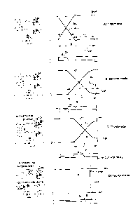
Figure 3 illustrates the equivalent circuit and waveforms for inverting modes
(a) to (d) of
a converter according to the present invention;
CA 02842648 2014-02-13
270717
Figure 4 a schematic drawing showing optional commutating conditions for a two
six-
pulse converters according to the present invention as configured for
operation in a point-
to-point HVDC transmission link with highly asymmetric bi-directional power
flow;
Figure 5 is a schematic drawing showing a six-pulse converter according to the
present
invention as configured for operating in a point-to-point HVDC transmission
link with bi-
directional power flow or as a terminal in a multi-terminal HVDC grid with bi-
directional
power flow;
Figure 6 is a schematic drawing showing a six-pulse converter according to the
present
invention as configured for operating in a point-to-point HVDC transmission
link with
bi-directional power flow or as a terminal in a multi-terminal HVDC grid with
uni-
directional power flow; and
Figure 7 is a schematic drawing showing a twelve-pulse converter according to
the
present invention connected to a symmetrical monopole point-to-point HVDC
transmission link with bi-directional power flow or a symmetrical monopole
multi-
terminal HVDC grid with bi-directional power flow.
With reference to Figures 1 and 4, a point-to-point HVDC transmission link
includes a
first current source converter (CSC) 2a and a second CSC 2b connected to first
and
second respective ends of an HVDC transmission line 4. Each CSC 2a, 2b is
shown as
being a three-phase transformer-fed type with an associated converter
transformer 6a, 6b,
series mode voltage source active filter (AF) 8a, 8b, shunt mode combined
active filter
and static compensator (AF StatCom) 10a, 10b, and dc link inductor 12a, 12b.
Surge
arresters and the control system are not shown in Figures 1 and 4 for reasons
of clarity.
Active filters and filter compensators are not shown in Figure 4 for reasons
of clarity.
With particular reference to Figure 4, each CSC 2a, 2b includes a bridge 14a,
14b. The
first bridge 14a has three ac terminals 16a, 16b, 16c (i.e., one for each
phase) connected
to the associated converter transformer 6a and two dc terminals 18a, 18b
connected to
one end of the HVDC transmission line 4. The second bridge 14b has three ac
terminals
21
CA 02842648 2014-02-13
270717
20a, 20b, 20c connected to the associated converter transformer 6b and two dc
terminals
22a, 22b connected to the other end of the HVDC transmission line 4.
Each bridge 14a, 14b includes a six converter arms. Each arm includes a first
reverse
blocking power semiconductor device ('first device' 24) which in practice can
be a
reverse blocking gate turn-off thyristor (GTO) or reverse blocking gate
commutated turn-
off thyristor (GCT), and a second power semiconductor device ('second device'
26)
which in practice can be a conventional thyristor. The first and second
devices 24, 26 are
connected together in anti-parallel, i.e., each first device has its anode
connected to the
respective ac terminal and its cathode connected to the respective dc terminal
and each
second device has its cathode connected to the respective ac terminal and its
anode
connected to the respective dc terminal.
Each converter arm can include any convenient number of series-connected first
devices
24 and series-connected second devices 26 to provide a bridge with a required
ac line
voltage rating. Groups of series-connected power semiconductor devices may be
assembled within modules and any convenient number of modules may be connected
in
series. Pressure contact power semiconductor devices may be used in order to
allow the
low resistance failure mode of such devices to be exploited as a means of
providing N+M
type series redundancy; where N series-connected devices have adequate total
voltage
rating for normal working and M additional devices are connected in series to
allow M
devices to fail without affecting the working behaviour of the N non-failed
devices.
Voltage sharing and synchronised switching is achieved using any combination
of
passive switching aid networks (RC type snubbers), voltage sharing resistors,
voltage
grading capacitors and di/dt limiting reactors, which may be of saturating
type. When
both first and second devices 24, 26 are employed, the current ratings of the
respective
parallel paths need not be equal and it may be advantageous to employ a large
level of
asymmetry in current rating.
22
CA 02842648 2014-02-13
270717
When power is controlled so as to flow from left to right in the arrangement
shown in
Figures 1 and 4, CSC 2a will operate as a rectifier and CSC 2b will operate as
an inverter
and vice versa.
When a CSC is operating as a rectifier, the first devices 24 are maintained in
an 'off' state
by gate control and the second devices 26 operate in a naturally commutated
rectifier
mode. When a converter is operating as an inverter, the second devices 26 are
not turned
'on' by gate control and the first devices 24 are operated in one of the three
inverting
modes (a) to (c) (and optionally also in mode (d)) described below with
reference to
Figure 3.
Figure 2 shows a multi-terminal HVDC grid with an HVDC transmission line 28.
CSC
2b is equivalent to CSC 2b of Figure 1, i.e., three-phase transformer-fed type
with first
and second devices connected in anti-parallel, and is connected to one end of
the HVDC
transmission line 28. CSC 2c is connected to another end of the HVDC
transmission line
28 and has a bridge according to the present invention that includes only
first devices
which in practice can be GTOs or GCTs that are operated in one of the three
inverting
modes (a) to (c) (and optionally also in mode (d)) described in more detail
below with
reference to Figure 3. CSC 2d is connected to another end of the HVDC
transmission
line 28 and has a bridge that includes only conventional thyristors that are
operated as a
rectifier. Each CSC has an associated converter transformer 6b, 6c, 6d, series
mode
voltage source active filter (AF) 8b, 8c, 8d, shunt mode combined active
filter and static
compensator (AF StatCom) 10b, 10c, 10d, and dc link inductor 12b, 12c, 12d.
Surge
arresters and the control system are not shown in Figure 2 for reasons of
clarity.
When power is controlled so as to flow from left to right from CSC 2d to CSC
2b in the
arrangement shown in Figure 2, CSC 2d will operate as a rectifier and CSC 2b
will
operate as an inverter. CSC 2c has no ability to transmit power from left to
right. When
power is controlled so as to flow from right to left from CSC 2b to CSC 2c,
CSC 2b with
operate as a rectifier and CSC 2c will operate as an inverter. CSC 2d has no
ability to
transmit power from right to left.
23
CA 02842648 2014-02-13
270717
When CSC 2b is operating as a rectifier, the first devices 24 are maintained
in an 'off
state by gate control and the second devices 26 operate in a naturally
commutated
rectifier mode. When CSC 2b is operating as an inverter, the second devices 26
are not
turned 'on' by gate control and the first devices 24 are operated in one of
the three
inverting modes (a) to (c) (and optionally also in mode (d)) described in more
detail
below with reference to Figure 3. When CSC 2c is operating, the first devices
are
operated in one of the three inverting modes (a) to (c) (and optionally also
in mode (d))
described in more detail below with reference to Figure 3. When CSC 2d is
operating,
the conventional thyristors operate in a naturally commutated rectifying mode.
Such a multi-terminal HVDC grid can employ any convenient number of converters
of
different types, including those that are conventional. An CSC according to
the present
invention can be configured with any desired degree of power flow asymmetry.
The four inverting modes (a) to (d) are described in more detail with respect
to Figure 3
which shows a simplified equivalent circuit of the respective inverting
commutation
mode on the left-hand side and the corresponding waveforms on the right-hand
side.
It will be readily appreciated that the waveforms of Figure 3 are not to scale
but allow
comparisons to be made. In each case, the dc link current Idc has the same
magnitude.
After commutation events in inverting modes (a) to (c) and subsequent
transient voltage
responses, the waveforms of outgoing device anode-cathode voltage Vak are
equivalent
to the ac line voltage between incoming and outgoing phases and have the same
magnitudes. A reference time is aligned to the zero crossing of the line
voltage. The
waveforms are all shown with respect to time. However, because the pulse
repetition
periods are substantially fixed according to the ac grid frequency which has
an equivalent
angular frequency, the elapsed times and relative positions of waveform events
can be
expressed as angles in the frequency domain. In the following description, the
time
reference is therefore defined in terms of a reference angle f3ref and the
incoming devices
are turned on at a point in time that is defined as a firing advance angle 13
as shown in
Figure 3.
24
CA 02842648 2014-02-13
270717
The firing sequences that are applied to the gate drivers of the incoming and
outgoing
devices are shown as logic signal waveforms gm and gout with logic levels
defined as
0=off and 1¨on. The logic waveforms gm and gout do not indicate the precise
voltage that
the gate drivers apply between the gate and cathode terminals of the incoming
and
outgoing devices, nor do they indicate the precise current that the gate
drivers apply to
the gate terminals of the incoming and outgoing devices. Yet it will be clear
that the gate
drivers must have a critical influence upon the behaviour of the devices. Mode
(c) and
optional mode (d) require that the outgoing devices receive a gate bias that
is negative
with respect to cathode at the time of gate commutation and that the gate
driver shall be
able to extract charge from the gate terminal of the device. More
particularly, unity gain
turn-off mode is preferred and this requires the diversion of anode current
from cathode
to gate. The gate drivers must therefore be designed so as to be capable of
causing a gate
current that is greater than the level of the anode current lama in the
outgoing devices to
be extracted from the gate terminal at the time of gate commutation. The gate
driver,
having been so designed, when operating in mode (b), and when instructed to
gate
commutate the associated outgoing device at the reference time Pref,
inherently prevents
so called 'forward recovery failure' of the outgoing device. The skilled
person will
understand that the outgoing device in a conventional LCC would suffer
'forward
recovery failure' if the available circuit commutated turn-off time tq is
shorter than the
recovery time of the device. However, with the appropriate gate drivers, the
devices used
in the converter of the present invention may routinely operate with an
available circuit
commutated turn-off time tq that is shorter than the recovery time that is
applicable with
an open circuit gate terminal bias applied.
The devices can optionally be optimised to minimise 'on' state voltage drop as
far as is
consistent with mode (b) and (c).
The devices can optionally be optimised to minimise 'on' state voltage drop as
far as is
consistent with modes (b) and (c) and one of: (i) single commutation events
according to
mode (d), and (ii) a maximum of ten successive commutation events according to
mode
CA 02842648 2014-02-13
270717
(d) having a repetition interval that is equal to the period of the associated
grid
fundamental frequency.
The equivalent circuit for mode (a) is directly equivalent to that of the
conventional line
commutated converter (LCC) and is included as a reference against which the
other
modes may be compared. The dc link current Idc flows in an ideal current
source whose
first terminal is connected to two ideal phase voltages. Each phase voltage
source has a
corresponding series-connected phase commutating reactance and reverse
blocking
power semiconductor device (GTO or GCT). The anode of each device is connected
to
the corresponding commutating reactance and the cathodes of the devices are
connected
together and to the second terminal of the ideal current source. The polarity
of the ac line
voltage (i.e., the difference between the two ac phase voltages) is such that
an incoming
device will carry anode current Iain when it is turned 'on' by gate control.
Referring now to the corresponding waveforms for mode (a), an incoming device
is
turned 'on' by gate control as shown by the 0-1 transition of gin for its
associated gate
driver (i.e., the gate driver is set to an 'on' state) at a firing advance
angle 13 relative to
reference angle Pref thereby initiating a commutation event. It will be
readily appreciated
that the commutation processes herein described are effectively a sequence of
such
commutation events according to a suitable control process. The anode current
Iain
carried by the incoming device will increase at a rate that is set by the
instantaneous sum
of the phase voltages divided by the sum of the phase commutating reactances ¨
taking
into consideration the mutual and leakage components of these reactances. The
anode
current Ikut in the outgoing device correspondingly decreases at a rate that
is equal and
opposite to that of the anode current Ian, in the incoming device. During the
time interval
defined by the commutation overlap angle II, the anode current Iain rises to
the value of
the dc link current Idc while the anode current Mout falls to zero. After the
commutation
overlap angle It, the anode-cathode voltage Vak appears as a reverse bias
voltage across
the outgoing device for a time interval defined by the available circuit
commutated turn-
off time which is labelled tq.
26
CA 02842648 2014-02-13
270717
Since the incoming device is now in the 'on' state and carries an anode
current Iam which
is equal to the dc link current Idc, the anode-cathode voltage Vak of the
outgoing device
is generally equal to the ac line voltage but experiences a negative going
transient
overshoot as a result of the combined action of the di/dt of the reverse
recovery of the
outgoing device and the damping factor of the commutated circuit upon the
voltage that
is developed across the commutating reactance. According to best practice, the
damping
factor of the commutated circuit will be influenced by the presence of
switching aid
networks (snubbers) which are invariably connected in parallel with reverse
blocking
power semiconductor devices of the types specified. The available circuit
commutated
turn-off time tq ends at the point when the anode-cathode voltage Vak reverses
and
reference angle Ref is set at this point in time. At the reference angle Pref,
the gate
driver for the outgoing device is set to the 'off' state as shown by the 1-0
transition in gout
and gate turn-off current is applied to the outgoing device. This has little
effect upon the
outgoing device because its anode-cathode voltage Vak has been reverse biased
for the
duration of the available circuit commutated turn-off time tq. It can be seen
that tql3-
and the outgoing device will reliably continue to block and withstand the
applied anode-
cathode voltage Vak providing the available circuit commutated turn-off time
tq is
greater than the recovery time of the outgoing device.
The equivalent circuit for mode (b) is identical to that for mode (a). The
waveforms for
mode (b) are similar to those for mode (a) and the only change is that the
available circuit
commutated turn-off time tq approaches zero. The effect of reducing firing
advance
angle 13 upon commutated di/dt and t is exaggerated and the available circuit
commutated
turn-off time tq is shown with a small, non-zero value in the interest of
clarity. As the
limit case of mode (b) (when tq=0, 13=p.) is approached, the progressive
reduction in
commutated di/dt that is a consequence of the sinusoidal nature of the phase
voltage
sources is such as to cause the reverse recovery current of the outgoing
device is the be
minimal, consequently a small anode-cathode voltage Vak transient is
experienced and
the corresponding turn-off switching loss is negligible. The magnitude of the
voltage
transient and corresponding turn-off switching loss reduce and power factor
increases as
27
CA 02842648 2014-02-13
270717
firing advance angle 13 is reduced towards the limit case at which the reverse
recovery
current of the outgoing device is suppressed and the power factor of the ac
line current is
then approximately defined by the cosine of a phase displacement angle which
is equal to
12. At the reference angle Pref, the gate driver for the outgoing device is
set to the 'off'
state as shown by the 1-0 transition in gout and gate turn-off current is
applied to the
outgoing device. This has a significant effect upon the outgoing device
because its
anode-cathode voltage Vak has been reverse biased for an available circuit
commutated
turn-off time tq that is shorter than the recovery time of the outgoing
device. Under these
conditions, the outgoing device contains significant stored charge which would
render it
unable to block the forward biased anode-cathode voltage Vak that is applied
at the
reference angle 13ref were it not for the beneficial effect of applying gate
turn-off current.
The exemplary variables depicted in Figure 4 that apply to the inverting
bridge in the
100% power flow left to right condition are for tq=0.63 s and for all
practical purposes
this is effectively equal to the limit condition of mode (b) where tq=0.
The firing advance angle 13 of the converter is significantly reduced relative
to the
limiting case for the conventional LCC whose available circuit commutated turn-
off time
tq=ii- must typically be greater than about 1.5 ms in order to achieve safe
commutation.
The limiting case for mode (b) is where tq=0 or where the firing advance angle
0 has a
limit case of pm. This means that the converter can be continuously operated
at a
greater power factor than a conventional LCC and a smaller power factor
correction
system can be employed. The converter also produces reduced harmonic forcing
voltage
so smaller ac- and dc-side harmonic filters are needed. Switching losses in
the devices
are reduced. In defining these benefits, it is necessary to recognise that, as
the limit case
of mode (b) is approached, reductions in the firing advance angle 13 cause
increases in the
commutation overlap angle and it is generally important that the upper limit
of
commutating inductance is no greater than is practically necessary.
The equivalent circuit for mode (c) includes a series RC type snubber in
parallel with the
outgoing device. In practice it might be expected that a suitable snubber will
be provided
28
CA 02842648 2014-02-13
270717
in parallel with each device (or with the anti-parallel connected pair of
devices) and they
have an influence on the transients in the anode-cathode voltage Vak that
arise following
gate commutation that occurs in modes (c) and (d).
The corresponding waveforms show mode (c) where conditions equivalent to
natural
commutation mode (a) or (b) have been initiated by turning 'on' an incoming
device at
firing advance angle 13 (i.e., the gate driver for the incoming device is set
to the 'on' state
as shown by the 0-1 transition of gin) and where gate commutation of the
outgoing device
is initiated at reference angle Pref (i.e., the gate driver for the outgoing
device is set the
'off' state as shown by the 1-0 transition of gout). During the period of the
firing advance
angle 13 the waveforms are similar to those shown for modes (a) and (b), i.e.,
the anode
current Iain carried by the incoming device will increase whilst the anode
current Tam in
the outgoing device correspondingly decreases. The commutation overlap angle
tt and
the available circuit commutated turn-off time tq are not directly relevant to
mode (c).
The advance firing angle 13 is normally chosen so that the anode current lam
in the
outgoing device is within acceptable limits at the time when gate commutation
is
initiated. Gate commutation of the anode current Ianin in the outgoing device
causes a
positive going transient in the anode-cathode voltage Vak whose magnitude is
determined
by the component values of the respective snubber, the value of the
commutation
reactance, the value of the anode current Tam immediately before gate
commutation and
the phase open circuit voltage. The magnitude of the anode-cathode voltage Vak
during
and immediately after gate commutation has a direct bearing on the magnitude
of the
turn-off switching loss of the outgoing device. Since the magnitude of the
commutating
reactance is fixed and there is a choice to be made in the timing of the
firing commands
to turn the devices 'on' an 'off', the critical role of the snubber in
defining the transient in
the anode-cathode voltage Vak is evident. Phase control of the firing advance
angle 13 is
used as the means of controlling the ratio between the dc and ac terminal
voltages of the
CSC and this control therefore has a bearing upon the turn-off condition of
the devices.
Since the stated objectives of the present invention require the commutation
process to
generate low power losses in order to maximise efficiency, it is generally
preferred that
29
CA 02842648 2014-02-13
270717
the timing of the commutation process and the design of the snubber are
optimised and
there is some flexibility in the choice of timing of both the advance firing
angle 13 and the
point in time of gate commutation. Accordingly the conditions depicted in
Figure 3 may
be altered so as to reduce the advance firing angle 13 and to initiate gate
turn-off of the
outgoing device after the reference angle Pref as long as the snubber is
appropriately
designed. When gate turn-off of the outgoing device is initiated after the
reference angle
13ref, the polarity of di/dt in incoming and outgoing devices reverses at the
reference angle
(3ref as a consequence of the sinusoidal nature of the phase voltage sources,
and thereafter
progressively increases causing the anode current Iaout in the outgoing device
to
correspondingly increase until interrupted at the point in time of gate
commutation. In
mode (c) the firing advance angle 13 of the CSC is significantly reduced
relative to the
limiting case for mode (b) and the available circuit commutated turn-off time
tq may be
considered to be negative. This means that the CSC can be continuously
operated at a
greater power factor than the conventional LLC and a smaller power factor
correction
system may be employed.
The equivalent circuit for mode (d) includes a non-liner resistive surge
arrestor in parallel
with the outgoing device. The incoming device has been omitted because it is
not turned
on. The magnitude of anode current that is gate commutated by the outgoing
device is
particularly high in mode (d) and the non-linear resistive surge arrester has
an influence
on the transients in the anode-cathode voltages yak that arise following gate
commutation at high values of anode current. When the surge arrester comprises
only
non-linear resistive elements, these have little or no influence on modes (a),
(b) or (c).
When the surge arrester comprises linear resistive and capacitive elements,
these have a
generally beneficial influence on modes (a), (b) and (c) in as much as they
may increase
the damping factor and reduce the peak magnitude of transients in the anode-
cathode
voltage Vak arising from commutation, thereby reducing switching losses in the
power
semiconductor switching devices. But in so doing they incur dissipation.
CA 02842648 2014-02-13
270717
The corresponding waveforms show the optional protective mode (d) where the
outgoing
device is turned 'off by gate commutation (i.e., the gate driver for the
outgoing device is
set to the 'off' state as shown by the 1-0 transition of gout) and without
having previously
initiated conditions equivalent to the natural commutation process of modes
(a) to (c).
The incoming device is not turned 'on' at a firing advance angle 13 (i.e., the
gate driver for
the incoming device remains in the 'off state as shown by gil, remaining at 0)
and the
outgoing device is turned 'off without its anode current Iaout having been
reduced from
the initial level of the dc link current Idc prior to gate commutation at the
reference angle
Pref or any other required angle. Whilst it is generally preferable to effect
gate
commutation at the reference angle 13ref because the instantaneous value of ac
line
voltage at that time is zero and because this is beneficial in reducing the
positive going
transient in the anode-cathode voltage Vak as a result of the increased
effectiveness of
snubbers and linear RC surge arresters (when used) in damping transient
voltages under
this condition, the gate commutation may optionally be effected at any
required time. For
example, in the event of a low impedance ac grid fault which causes dc link
current Idc to
increase rapidly beyond its rated level, it would then become preferable to
effect gate
commutation at the point in time when the dc link current Idc reached the
maximum
designed protective level. Since the snubber of the outgoing device is
preferably
optimised on the basis of gate commutation of an anode current Iaout having a
magnitude
that is much less than the dc link current Idc, the positive going transient
in the anode-
cathode voltage Vak is often greater than that which could be safely moderated
by the
snubber alone when the outgoing device is turned 'off. Accordingly the ac
lines
connected to the ac terminals of the CSC typically benefit from the voltage
limiting
behaviour of the non-linear surge arresters and optional linear resistive
capacitive surge
arresters mentioned above. Although the optional linear resistive capacitive
surge
arresters have a similar behaviour to the snubber of the outgoing device and
are generally
beneficial as described above, they are less effective than non-linear surge
arresters in
limiting peak voltage, particularly when dc link current Idc is increased to
fault levels.
When the outgoing device turns 'off, its anode current Iaout diverts into the
non-linear
surge arrester and the transient in the anode-cathode voltage Vak has a
truncated top
31
CA 02842648 2014-02-13
270717
whose peak magnitude is set by the breakover voltage and slope resistance of
the non-
linear surge arrester. The previously-described snubber and the optional
linear resistive
capacitive surge arrester is still effective in limiting the rates of increase
and decrease of
the transient in the anode-cathode voltage Vak. The anode-cathode voltage Vak
remains
at a low value after the transient because the ac line voltage is low under
short circuit
fault conditions. Mode (d) is a protective mode and is not intended to be
employed in a
sustained manner or under normal ac line voltage conditions. As shown in the
waveforms, an incoming device is not turned 'on' and the energy that is stored
in the dc
link reactor must be prevented from causing an additional voltage transient
component of
the anode-cathode voltage Vak. The preventative means can be provided by a
thyristor
clamp circuit which causes the dc link current Idc to divert into the clamp
and for this
current Iclamp to circulate in the loop comprising the dc link reactor and the
clamp. The
ideal current source Idc in the equivalent circuit represents the dc link
reactance and Vdc
is an ideal voltage source that represents the open circuit voltage of the dc
link. The dc
link will incorporate stray inductance and this is prevented from causing a
further
additional voltage transient component of the anode-cathode voltage Vak by dc
line surge
arresters that are connected across Vdc. Optionally, the CSC may be permitted
to
continue commutating repetitively for a period of time (typically 150 ms)
until the fault is
interrupted by a HVAC circuit breaker. If this optional protective strategy is
employed,
the incoming device is turned 'on' immediately before the outgoing device is
turned 'off',
thereby causing the anode current Mout in the outgoing device to divert into
the incoming
device rather than into the thyristor clamp circuit, the ac line surge
arrester in any case
remaining effective. The transient in the anode-cathode voltage Vak has a
truncated top
whose peak magnitude is set by the breakover voltage and slope resistance of
the ac line
surge arrester. The waveforms of the optional protective strategy are similar
to those of
the preferred protection strategy and are not shown; the only difference being
that the
anode current waveform of the incoming device is approximately the same as
that of
Iclamp which it replaces. The thyristor voltage clamp circuit must be retained
in order to
limit the dc voltage transient that is a consequence of the eventual
interruption of ac line
current by the HVAC circuit breaker.
32
CA 02842648 2014-02-13
270717
The operation of rectifying and inverting modes for highly asymmetric bi-
directional
power flow are now further explained with reference to Figure 4 which shows
CSCs 2a,
2b with first devices 24 (e.g., GTOs or GCTs) and second devices 26 (e.g.,
thyristors)
connected in anti-parallel.
The upper schematic is annotated with exemplary variables relating to 100%
power flow
from left to right, e.g., from CSC 2a to CSC 2b, whilst the lower schematic is
annotated
with exemplary variables relating to 1% power flow from right to left, e.g.,
from CSC 2b
to CSC 2a. In a practical example for a point-to-point HVDC transmission link
then CSC
2a might be receiving power from a plurality of offshore wind turbines, where
power is
supplied along the HVDC transmission link 4 to an ac grid or power network
connected
to CSC 2b. The HVDC transmission link 4 will normally operate with power flow
from
left to right. However, in some circumstances, a small amount of power (e.g.,
1% of the
typical power flow during normal operating conditions) might be provided to
the wind
turbines such that the direction of power flow is from right to left. As is
always the case
with a point-to-point HVDC transmission link, the HVDC transmission link
voltage may
be operated at any desired level that is consistent with the requirement to
maintain the
required power flow whilst respective HVAC grid voltages are maintained within
specified limits. Unusually, the CSC of the present invention can achieve the
required
reversible power flow without recourse to a reversal in HVDC transmission link
voltage.
It is inevitable that the conductors or cables of the HVDC transmission link
experience
resistive voltage drop variations that are pro rata with HVDC transmission
link current
and, although the exemplary HVDC transmission link voltage is subject to a
small
variation as power flow is reversed, the HVDC transmission link voltage is
substantially
constant. The exemplary HVDC transmission link current is therefore
approximately
proportional to power flow and has a polarity that corresponds with that of
power flow.
In both the upper and lower schematics of Figure 4, the left-hand HVAC grid
voltage has
been set at an arbitrary 290 kV and the right-hand HVAC grid voltage has been
set at an
arbitrary 266 kV.
33
CA 02842648 2014-02-13
270717
In the upper schematic of Figure 4, CSC 2a operates in rectifying mode with
the second
devices 26 under phase control and first devices 24 continuously gated in the
'off' state.
The thyristor firing delay angle a is 7 and the commutation overlap angle y
is 22.2 . It
would not be practical to operate CSC 2a phased any further forwards and the
commutation overlap angle is determined by the presence of full load current
and the
converter transformer reactance, which in this example is 12%. CSC 2a
therefore
operates at the best possible power factor. In some cases it might be
advantageous for a
small leading power factor correction to be applied by other equipment.
CSC 2b operates the first devices 24 under phase control in the naturally
commutated
inverting mode (b) with zero turn-off (ZTO). The second devices 26 are pulse
suppressed, i.e., they do not receive a gate drive current, so that they
remain in the 'off
state. The firing advance angle 13 is 28.36 and the commutation overlap angle
g is
28.34 . It would not be practical to operate CSC 2b phased any further back
and the
commutation overlap angle is determined by the presence of full load current
and the
converter transformer reactance, which in this example is 12%. CSC 2b
therefore
operates at the best possible power factor. In some cases it might be
advantageous for a
small leading power factor correction to be applied by other equipment. CSC 2b
operates
with an available circuit commutated turn-off time tq of 0.63iis which is
substantially
equal to the ZTO limit case condition.
In the lower schematic of Figure 4, CSC 2b operates in rectifying mode with
the second
devices 26 under phase control and first devices 24 continuously gated in the
'off state.
The thyristor firing delay angle a is 10 and the commutation overlap angle y
is
negligible. It would not be practical to operate CSC 2b phased any further
forwards.
CSC 2b therefore operates at the best possible power factor. There is no
significant
benefit to be gained from power factor correction since the lagging MVAR drawn
from
the ac grid is minimal at such a high power factor and a low power.
CSC 2a operates the first devices 24 under phase control in the naturally
commutated
inverting mode (b) with available circuit commutated turn-off time tq being
substantially
34
CA 02842648 2014-02-13
270717
shorter than the recovery time that is applicable with an open circuit gate
terminal bias
applied and the ZTO capability of the first devices 24 is therefore exploited.
The second
devices 26 are pulse suppressed, i.e., they do not receive a gate drive
current, so that they
remain in the 'off' state. The firing advance angle 13 is 27 and the
commutation overlap
angle pt is negligible. It would not be practical to operate CSC 2a phased any
further
back because the left-hand HVAC grid voltage would deviate from the above
arbitrarily
determined level of 290 kV. CSC 2a therefore operates at the best possible
power factor.
In some cases it might be advantageous for a small leading power factor
correction to be
applied by other equipment. CSC 2a operates with available circuit commutated
turn-off
time tq of 1243 !is which is significantly in excess of the ZTO limit case
condition but is
shorter than the required nominal 1500 las for natural commutation using
conventional
thyristors.
The exemplary conditions of Figure 4 include a high degree of asymmetry in
current
ratings and it would be possible to employ first devices 24 with a relatively
small current
rating in CSC 2a and second devices 26 with a relatively small current rating
in CSC 2b.
It would be within the scope of the present invention to operate the first
devices 24 of
CSC 2b with a reduced value of firing advance angle 13 according to mode (c),
i.e., the
combined naturally commutated and gate commutated inverting mode, for a power
flow
direction from left to right, as long as the rated working HVAC grid voltage
was adjusted
accordingly. CSC 2b would operate at an increased power factor when operating
under
the circumstances defined by mode (c) but this would be achieved at the
expense of
increased snubber component ratings and turn-off switching power losses in the
first
devices 24.
Although it might appear that the benefit of increased power factor would be
subject to a
simple trade off against increased snubber component cost and reduced
converter
efficiency, it must be recognised that the effect of improving power factor
also has a
direct bearing upon the volt.amp product of the CSC. In other words, the
converter
power rating that is achieved for a given HVAC line current and voltage rating
is
CA 02842648 2014-02-13
270717
effectively proportional to power factor. This means that the use of mode (c)
can be both
cost-effective and beneficial in terms of operational flexibility.
Figure 5 shows a schematic of the six-pulse CSC 2a shown in Figures 1 and 4.
The
bridge 14a includes three ac terminals 16a, 16b, 16c and first and second dc
terminals
18a, 18b. The ac terminals 16a, 16b, 16c are connected to an HVAC grid or
distribution
network by means of a converter transformer 6a.
Non-linear surge arrestors 30 are connected to the ac lines.
The de terminals 18a, 18b are connected to a respective conductor or cable of
the HVDC
transmission link 4 by means of HVDC link reactors 12a. A thyristor clamp
circuit 32 is
in parallel with the HVDC link reactors 12a ¨ see the detailed description of
mode (d)
above. A surge arrester 72 can be connected across the HVDC transmission link
4 to
prevent the stray inductance in the HVDC transmission link from causing an
additional
voltage transient component in the anode-cathode voltage Vak.
The converter transformer 6a includes grid-side windings 34 connected to the
three-phase
HVAC grid and converter-side windings 36 ¨ both of which are shown more
clearly in
the detail view. The converter-side windings 36 are effectively a star winding
whose
points of common coupling have been disconnected to provide three terminals
that are
connected to a three-phase series mode voltage source active filter (AF) 8a.
The series
mode active filter 8a may be of any convenient type, for example two-level,
three-level or
multi-level voltage source inverter. When the series mode active filter 8a is
controlled so
as to produce three-phase zero states (i.e., states where all line voltages
are set to zero)
the converter-side windings of the converter transformer 6a is effectively
star connected
with the series mode active filter effectively behaving as a star point. When
the CSC 2a
operates in any of mode (a) to (c) and the series mode active filter 6a is
controlled so as to
effectively behave as a star point, the ac terminals of the CSC 2a receive ac
voltages that
have the same harmonic relationship with the respective dc terminal voltages
and with the
HVAC grid voltages that is applicable to the conventional LCC. Under these
conditions
36
CA 02842648 2014-02-13
270717
the voltage between the dc terminals 18a, 18b includes a dominant dc component
upon
which is superimposed a spectrum of harmonic components of order np*Fg whose
amplitudes reduce as harmonic order increases, where p is the pulse number
(six in this
example), n=1, 2, 3.. .co, and Fg is the HVAC grid fundamental frequency.
These un-
filtered voltage harmonics are undesirable because they cause a corresponding
spectrum
of harmonic current components to flow in the HVDC transmission link 4 and
they may
be mitigated to a similar extent to that in the conventional LCC by the use of
the dc link
reactors 12a. The dominant harmonic component of HVDC transmission link
current is
that at six times the HVAC grid fundamental frequency. Since the CSC 2a may be
designed to operate with a smaller rectifier firing delay angle a or inverter
firing advance
angle f3 than in the conventional LCC, its HVDC transmission link current
ripple has
reduced amplitude. The current ripple can be reduced by increasing the HVDC
transmission link reactor inductance and the lowest order harmonic components
may be
eliminated by increasing the pulse number, for example, a twelve-pulse series
CSC (as
described below with reference to Figure 7) has a dc current ripple comprising
component of twelve times HVAC grid frequency and multiples therefore, while a
twenty-four-pulse series CSC has a dc current ripple comprising components of
twenty-
four times HVAC grid frequency and multiples thereof. Despite the possibility
of using
increased HVDC transmission link reactor inductance and converter pulse
number, this
approach entails an increase in the cost and complexity of wound components
and it may
be preferable to minimise this current ripple by active means. These active
means can be
provided by the series mode active filter 6a.
The series mode active filter 6a may be used to superimpose voltages upon the
ac line
voltages and thereby to effectively superimpose dc ripple voltages upon the
voltage
between the dc terminals 18a, 18b of the CSC 2a. The effectively superimposed
dc ripple
voltages may be controlled so as to be in anti-phase with the underlying
ripple dc voltage
that exists when the series mode active filter 6a acts as transformer star
point. The series
mode active filter 6a shown in Figure 5 has only three terminals and the
requirement for
symmetry in the three phases of the CSC 2a therefore constrain the active
filter to have
37
CA 02842648 2014-02-13
270717
no net power flow into or out of the active filter converter on average,
excluding a
fractionally small difference which is required to supply the power losses of
the active
filter converter. In its most basic form the preferred function of a
particular series mode
active filter is to oppose each positive going peak in the underlying dc
ripple voltage and
in doing so the active filter is receiving power from the HVAC grid in the
case where the
CSC 2a is operating as a rectifier. It follows that the series mode active
filter must export
power into the HVDC output by opposing each negative going peak in the
underlying dc
ripple voltage in order to satisfy the above requirement for zero net average
power flow
into the active filter. In its most basic form the series mode active filter
may superimpose
one positive going and one negative going rectangular pulse of voltage per
cycle of the
underlying ripple dc voltage (1/6th of a cycle of HVAC grid fundamental
frequency)
upon the voltage between the dc terminals 18a, 18b of the CSC 2a. The series
mode
active filter 6a may optionally superimpose a filtered or un-filtered pulse
width
modulated or staircase or other multi-level voltage waveform in order to more
comprehensively and precisely counteract the effects of dc voltage ripple upon
dc current
ripple. The use of the series mode active filter 6a allows the inductance,
size and cost of
the dc link reactors 12a to be reduced for a given permitted dc ripple current
content and,
moreover, the energy that is stored in the dc link reactors during over-
current faults may
be minimised.
A shunt mode active filter/compensator 10a may be included as shown in Figures
1 and 5
which is connected in parallel with the CSC 2a and on the grid-side of the
converter
transformer 6a. The active filter component will mitigate the injection of
current
harmonics of the fundamental frequency from the CSC 2a into the HVAC grid by
superimposing corresponding current harmonics onto the grid connection which
are
comparable in magnitude but in anti-phase to those generated in the CSC and
present on
the grid-side of the converter transformer 6a. The harmonic numbers h which
are
compensated by the active filter will depend on the pulse number of the CSC
but can be
described in general by h = (np 1) where p is the pulse number (6, 12, 18,
24 etc.) and
n--1, 2, 3...y, where y is determined by the grid harmonic injection
limitations which may
38
CA 02842648 2014-02-13
270717
be specific to the local requirements at the point of connection to the HVAC
grid. In
instances where the coupling of the CSC 2a to the HVAC grid or distribution
network
will result in particularly high levels of harmonics injection, it may be
beneficial to
include optional switched passive harmonic filters to provide additional
filtering and
reduce the rating requirements of the active filter.
The active filter may comprise any convenient three-phase active filter
implementation
and will typically include the benefit of controllable power factor
compensation at the
point of common coupling with the HVAC grid. Control of the compensator can be
accomplished by monitoring the phase displacement between the voltage and
injected
current at the point of common coupling into the ac grid such that the
required level of
reactive power may be injected by the compensator to achieve the required
power factor.
It has been noted that the CSC 2a will reduce the power factor compensation
requirements to the benefit of the compensator rating requirements when
compared to a
conventional LCC. The compensator rating requirements may be further reduced
by the
inclusion of power factor correction capacitors 38 connected in parallel to
the active
filter/compensator. These capacitors 38 may be continuously connected to the
HVAC
grid or may be connected in series with a suitable switching mechanism such
that their
inclusion and their cumulative reactive power compensation may be controlled.
Power provided to and received from the HVAC grid to the active
filter/compensator 10a
may be such that on average a balance is achieved and no net power is supplied
to the
CSC 2a; excluding a fractionally small difference which is required to supply
the active
filter/compensator losses. It has been identified that in some instances it
may be
optionally beneficial for the CSC 2a to pre-energise the converter transformer
6a, to pre-
synchronise to the HVAC grid before ac circuit breaker closure, and to
potentially 'black-
start' an `islanded' HVAC grid. In this instance, the commutating voltage
required by the
CSC 2a may be provided by the active filter/compensator 10a if a suitable
energy source
is coupled to the dc link of the active filter/compensator. This may include
any
convenient means of providing reserve power including through standby
generation or by
39
CA 02842648 2014-02-13
270717
the inclusion of a mechanism of energy storage with sufficient storage
capacity to supply
energy for the duration required by the specific instance of implementation of
the CSC
2a.
The active filter/compensator 10a may be directly coupled to the HVAC grid or
optionally coupled to the HVAC grid via an isolating transformer 40 which will
provide
an additional level of protection to the active filter/compensator during
possible fault
conditions on the HVAC grid and whose voltage step-up capability would allow
for a
more convenient lower voltage operation of the active filter/compensator. The
active
filter 10a can include a pulse width modulated (PWM) filter whose function is
to
minimise the propagation of active filter switching frequency harmonics into
the ac grid.
Transformer 40 and power factor correction capacitors 38, if provided, may
supplement
or replace the PWM filter.
Figure 6 shows a schematic of the six-pulse CSC 2c shown in Figure 2. The CSC
2c is
similar to CSC 2a but the bridge 14c includes only first devices 24 (e.g. GTOs
or GCTs)
and it can operate only as an inverter when first dc terminal 44a is positive
with respect to
second dc terminal 44b. The skilled person will appreciate that if the voltage
between dc
terminals 44a and 44b are reversed, then a CSC according to the present
invention
including only first devices may optionally operate as a rectifier since GTOs
and GCTs
are inherently capable of thyristor-like behaviour when provided with
appropriate gate
drive. The bridge 14c includes three ac terminals 42a, 42b, 42c. The ac
terminals 42a,
42b, 42c are connected to an HVAC grid or distribution network by means of a
converter
transformer 6c.
Non-linear surge arrestors 46 are connected to the ac lines.
The dc terminals 44a, 44b are connected to a respective conductor or cable of
the HVDC
transmission link 28 by means of HVDC link reactors 12c. A thyristor clamp
circuit 48 is
in parallel with the HVDC link reactors 12c ¨ see the detailed description of
mode (d)
above. A surge arrester 72 can be connected across the HVDC transmission link
28 to
CA 02842648 2014-02-13
270717
prevent the stray inductance in the HVDC transmission link from causing an
additional
voltage transient component in the anode-cathode voltage Vak.
The converter transformer 6c includes grid-side windings connected to the
three-phase
HVAC grid and converter-side windings. The converter-side windings are as
described
above for converter transformer 6a and are connected to a three-phase series
mode
voltage source active filter (AF) 8c. The series mode active filter 8c
operates in the same
way as the series mode active filter 8a described above.
A shunt mode active filter/compensator 10c is connected in parallel with the
CSC 2c on
the grid-side of the converter transformer 6c. The active filter/compensator
10c operates
in the same way as the active filter/compensator 10a described above. The
compensator
rating requirements may be further reduced by the inclusion of power factor
correction
capacitors 50 connected in parallel to the active filter/compensator. The
active
filter/compensator 10c may be directly coupled to the HVAC grid or optionally
coupled
to the HVAC grid via an isolating transformer 52. The active
filter/compensator 10c can
include a PWM filter whose function is to minimise the propagation of active
filter
switching frequency harmonics into the HVAC grid. Transformer 52 and power
factor
correction capacitors 50, if provided, may supplement or replace the PWM
filter.
Figure 7 shows a schematic of a twelve pulse CSC 2e with first and second
bridges 54,
56. The first bridge 54 includes three ac terminals 58a, 58b, 58c and first
and second dc
terminals 60a, 60b. The second bridge 56 includes three ac terminals 62a, 62b,
62c and
first and second dc terminals 64a, 64b. The ac terminals 58a, 58b, 58c of the
first bridge
54 and the ac terminals 62a, 62b, 62c of the second bridge 56 are connected to
an HVAC
grid or distribution network by means of a converter transformer assembly 64.
The first
dc terminal 60a of the first bridge 54 defines a first dc terminal of the CSC
2e and is
connected to a conductor or cable of the HVDC transmission link 66 by means of
a
HVDC link reactor 68. The second dc terminal 64b of the second bridge 56
defines a
second dc terminal of the CSC 2e and is connected to a conductor or cable of
the HVDC
transmission link 66 by means of a HVDC link reactor 68. A thyristor clamp
circuit 70 is
41
CA 02842648 2014-02-13
270717
in parallel with each HVDC link reactor 68 ¨ see the detailed description of
mode (d)
above.
The second dc terminal 60b of the first bridge 54 and the first dc terminal
64a of the
second bridge 56 are connected together and to ground by means of a grounding
resistor
84.
A surge arrester 72 is connected between the first and second dc terminals
60a, 60b of the
first bridge 54 and a surge arrester 72 is connected between the first and
second dc
terminals 64a, 64b of the second bridge 56 in order to prevent the stray
inductance in the
HVDC transmission link from causing an additional voltage transient component
in the
anode-cathode voltage Yak. If the protection strategy of CSC 2e is such that
mode (d) is
effected simultaneously in both the first and second bridges 54, 56, then a
single surge
arrester may optionally be connected across the HVDC transmission link instead
of the
two specified surge arresters 72.
Each converter arm includes a first device 24 (e.g., a GTO or GCT) and a
second device
26 (e.g., a thyristor) connected in anti-parallel. The CSC 2e is therefore
capable of
operating as both a rectifier and an inverter with bi-directional power flow
through the
HVDC transmission link 66 without requiring a voltage reversal.
The phase-shifting converter transformer assembly 64 is shown as being two
discrete
transformers 74a, 74b. Each transformer 74a, 74b includes grid-side windings
connected
to the three-phase HVAC grid and converter-side windings. A first transformer
74a has a
star connected grid-side winding and a star connected converter-side winding
whose
points of common coupling have been disconnected to provide three terminals
that are
connected to a first three-phase series mode voltage source active filter (AF)
76a. A
second transformer 74b has a delta connected grid-side winding and a star
connected
converter-side winding whose points of common coupling have been disconnected
to
provide three terminals that are connected to a second three-phase series mode
voltage
source active filter 76b. The respective converter-side windings have
identical rated
42
CA 02842648 2014-02-13
270717
voltage magnitudes and impedances relative to the grid-side point of common
coupling
but the voltages are subject to a 30 relative phase shift as will be
understood by the
skilled person. The first and second series mode active filters 76a, 76b may
be of any
convenient type, for example two-level, three-level or multi-level voltage
source
inverters. When the first and second series mode active filters 76a, 76b are
controlled so
as to produce their respective three-phase zero states (i.e., states where all
line voltages
are set to zero) the respective converter-side windings of each transformer
74a, 74b are
effectively star connected with the series mode active filters effectively
behaving as star
points. When the CSC 2e operates in any of modes (a) to (c) and the first and
second
series mode active filters 76a, 76b are controlled so as to effectively behave
as a star
point, the ac terminals of the CSC 2e receive ac voltages that have the same
harmonic
relationship with the respective dc terminal voltages and with the HVAC grid
voltages
that are applicable to the conventional LCC. Under these conditions the
voltage between
the first and second d- terminals of the CSC 2e includes a dominant dc
component upon
which is superimposed a spectrum of harmonic components of order np*Fg whose
amplitudes reduce as harmonic order increases, where p is the pulse number
(twelve in
this example), n=1, 2, 3...00, and Fg is the HVAC grid fundamental frequency.
These un-
filtered voltage harmonics are undesirable because they cause a corresponding
spectrum
of harmonic current components to flow in the HVDC transmission link 66 and
they may
be mitigated to a similar extent to that in the conventional LCC by the use of
the dc link
reactors 68. The dominant harmonic component of HVDC transmission link current
is
that at twelve times the HVAC grid fundamental frequency. Since the CSC 2e may
be
designed to operate with a smaller rectifier firing delay angle a or inverter
firing advance
angle 13 than in the conventional LCC, its HVDC transmission link current
ripple has
reduced amplitude. The current ripple can be reduced by increasing the HVDC
transmission link reactor inductance and the lowest order harmonic components
may be
eliminated by increasing the pulse number, for example, a twenty-four-pulse
series CSC
has a dc current ripple comprising components of twenty-four times HVAC grid
frequency and multiples thereof. Despite the possibility of using increased
HVDC
transmission link reactor inductance and converter pulse number, this approach
entails an
43
CA 02842648 2014-02-13
270717
increase in the cost and complexity of wound components and it may be
preferable to
minimise this current ripple by active means. These active means can be
provided by the
first and second series mode active filters 76a, 76b.
The first and second series mode active filters 76a, 76b may be used to
superimpose
voltages upon the ac line voltages and thereby to effectively superimpose dc
ripple
voltages upon the voltage between the first and second de terminals of the CSC
2e. The
effectively superimposed dc ripple voltages may be controlled so as to be in
anti-phase
with the underlying ripple dc voltage that exists when the first and second
series mode
active filters 76a, 76b act as transformer star points. The series mode active
filters 76a,
76b shown in Figure 7 each have only three terminals and the requirement for
symmetry
in the three phases of the CSC 2e therefore constrain each active filter to
have no net
power flow into or out of the active filter converter on average, excluding a
fractionally
small difference which is required to supply the power losses of the active
filter
converter. In its most basic form the preferred function of a particular
series mode active
filter is to oppose each positive going peak in the underlying dc ripple
voltage of the
respective bridge and in doing so that particular active filter is receiving
power from the
HVAC grid in the case where the CSC 2e is operating as a rectifier. It follows
that the
same series mode active filter must export power into the HVDC output by
opposing
each negative going peak in the underlying dc ripple voltage of the respective
bridge in
order to satisfy the above requirement for zero net average power flow into
the active
filter. In its most basic form the series mode active filter may superimpose
one positive
going and one negative going rectangular pulse of voltage per cycle of the
underlying
ripple dc voltage of the respective bridge (1/6th of a cycle of HVAC grid
fundamental
frequency) upon the voltage between the dc terminals of the respective bridge
of the CSC
2e. The series mode active filter may optionally superimpose a filtered or un-
filtered
pulse width modulated or staircase or other multi-level voltage waveform in
order to
more comprehensively and precisely counteract the effects of dc voltage ripple
upon
current ripple. The harmonic corrective voltages that are developed within
first and
second series mode active filters 76a, 76b are symmetrically interleaved by
defining that
44
CA 02842648 2014-02-13
270717
they benefit from the same 30 of grid fundamental frequency phase shift that
is applied
to the phase controlled events of the first and second bridges 54, 56. The use
of the series
mode active filters 76a, 76b allows the inductance, size and cost of the dc
link reactors 68
to be reduced for a given permitted dc ripple current content and, moreover,
the energy
that is stored in the dc link reactors during over-current faults may be
minimised.
Non-linear surge arrestors 78a are connected to the ac lines of the first
bridge 54 and non-
liner surge arrestors 78b are connected to the ac lines of the second bridge
56.
A common shunt mode active filter/compensator 78 may be included as shown in
Figure
7 which is connected in parallel with the CSC 2e on the grid-side of the
converter
transformer assembly 64. The active filter component will mitigate the
injection of
harmonics of the fundamental frequency from the CSC 2e into the HVAC grid by
superimposing matching current harmonics onto the grid connection which are
comparable in magnitude but in anti-phase to those generated in the CSC and
present on
the grid-side of the converter transformer assembly 64. The harmonic numbers h
which
are compensated by the active filter are in accordance with the pulse number
of the CSC
but can be described by h = (12n 1) n=1, 2, 3...y, where y is determined by
the grid
harmonic injection limitations which may be specific to the local requirements
at the
point of connection to the HVAC grid. In instances where the coupling of the
CSC 2e to
the HVAC grid or distribution network will result in particularly high levels
of harmonic
injection, it may be beneficial to include optional switched passive harmonic
filters to
provide additional filtering and reduce the rating requirements of the active
filter.
The active filter may comprise of any convenient three-phase active filter
implementation
and will typically include the benefit of controllable power factor
compensation at the
point of common coupling with the HVAC grid. Control of the compensator can be
accomplished by monitoring the phase displacement between the voltage and
injected
current at the point of common coupling such that the required level of
reactive power
may be injected by the compensator to achieve the required power factor. It
has been
noted that the CSC 2e will reduce the power factor compensation requirements
to the
CA 02842648 2014-02-13
270717
benefit of the compensator rating requirements when compared to a conventional
LCC.
The compensator rating requirements may be further reduced by the inclusion of
power
factor correction capacitors 80 connected in parallel to the active
filter/compensator.
These capacitors 80 may be continuously connected to the HVAC grid or may be
connected in series with a suitable switching mechanism such that their
inclusion and
their cumulative reactive power compensation may be controlled.
Power provided to and received from the HVAC grid to the active
filter/compensator 78
may be such that on average a balance is achieved and no net power is supplied
to the
CSC 2e; excluding a fractionally small difference which is required to supply
the active
filter/compensator losses. It has been identified that in some instances it
may be
optionally beneficial for the CSC 2e to pre-energise the converter transformer
assembly
64, to pre-synchronise to the HVAC grid before ac circuit breaker closure, and
to
potentially 'black-start' an `islanded' HVAC grid. In this instance, the
commutating
voltage required by the CSC 2e may be provided by the active
filter/compensator 78 if a
suitable energy source is coupled to the dc link of the active
filter/compensator. This
may include any convenient means of providing reserve power including through
standby
generation or by the inclusion of a mechanism of energy storage with
sufficient storage
capacity to supply energy for the duration required by the specific instance
of
implementation of the CSC 2e.
The active filter/compensator 78 may be directly coupled to the HVAC grid or
optionally
coupled to the HVAC grid via an isolating transformer 82 which will provide an
additional level of protection to the active filter/compensator during
possible fault
conditions on the HVAC grid and whose voltage step-up capability would allow
for a
more convenient lower voltage operation of the active filter/compensator.
The active filter/compensator 78 can include a PWM filter whose function is to
minimise
the propagation of active filter switching frequency harmonics into the ac
grid.
Transformer 82 and power factor correction capacitors 80, if provided, may
supplement
or replace the PWM filter.
46