Note : Les descriptions sont présentées dans la langue officielle dans laquelle elles ont été soumises.
CA 02843203 2014-01-27
WO 2013/026697 PCT/EP2012/065433
1
Description
Technical field of the invention
RFID chip module
The invention pertains to chip modules, particularly to RFID chip modules for
connecting to textile substrates. The invention pertains further to a label
having an
RFID chip module and to a method of manufacturing a label having an RFID chip
module.
Background
RFID chips have become increasingly useful for labelling textiles, for example
-15 clothing or other products made from textiles. In order to ensure their
proper
functionality RFID labels have to be provided with an RFID transponder chip
and a
corresponding antenna structure for sending and receiving electrical RF1D
signals.
RFID labels may be manufactured by using an RFID chip and connecting the
RFID chip to an electrically conductive strip in a substrate, such as a
textile
substrate having a metal strip glued to or woven therein.
Since RFID labels are a mass product there is a need for efficiently and
reliably
manufacturing RFID labels with a high throughput.
Summary
An idea of the present invention is to provide a chip module, particularly an
RFID
chip module, for connecting to a substrate having an antenna structure, for
example a textile substrate with a metallization structure forming an RFID
antenna.
In order to reliably and efficiently connect the chip module to the substrate,
the
chip module is provided with a metallization structure on the bottom side,
which
may be soldered to the metallization structure of the substrate. The soldering
may
be performed by a laser reflow soldering process, wherein the chip module is
irradiated on the surface opposite to the surface with the metallization
structure by
one or more laser beams, which are guided through the main body of the chip
module towards the metallization structure. The energy of the laser beams may
be
deposited mainly at the metallization structure in order to reflow soldering
material
CA 02843203 2014-01-27
WO 2013/026697
PCT/EP2012/065433
2
arranged on the metallization structure, thus forming a solder connection
between
the chip module and the substrate.
An aspect of the present invention therefore relates to a chip module
according to
independent claim 1. The chip module comprises a carrier, having a first main
surface and a second main surface opposite to the first main surface, a first
recess
structure arranged in the carrier in the first main surface, and a chip
arranged in
the first recess structure of the carrier. A patterned metallization layer is
deposited
on the second main surface of the carrier, the metallization layer having a
first
metallization structure and a second metallization structure, the first
metallization
structure being electrically isolated from the second metallization structure.
The
chip is electrically connected to the first metallization structure and the
second
metallization structure.
With the chip module according to claim 1 a fast, efficient and reliable laser
reflow
soldering process may be used when soldering the chip module to a substrate.
One of several advantages consists in the chip module being configured to
guide
energy from laser beams hitting the first main surface through the carrier to
the
metallization structure, where a soldering process may be performed. The
possibility of laser reflow soldering through the main body of the chip module
increases the processing speed and efficiency.
According to one embodiment the carrier may comprise a material which is
transparent to visible, UV, and/or infrared light. This provides the advantage
that
the energy of laser beams used for laser reflow soldering are not or not
substantially absorbed in the carrier material, thus providing for a faster
reflow
process.
According to another embodiment the chip module may comprise a second recess
structure arranged in the carrier in the first main surface opposite to the
first
metallization structure, and a third recess structure arranged in the carrier
in the
first main surface opposite to the second metallization structure. The
additional
recess structures provide the advantage that the thickness of the carrier is
lower in
the areas where a laser beam is guided through the carrier of the chip module.
Advantageously, the second and the third recess structures may be vias which
extend from the first main surface to the second main surface through the
carrier.
CA 02843203 2014-01-27
WO 2013/026697
PCT/EP2012/065433
3
This allows for a direct energy transfer of the laser beams to the
metallization
structure on the surface of the carrier, when laser beams are guided through
the
vias.
In an embodiment, the vias may extend through the first and the second
metallization structures. In this case, the energy of the laser beams is
directly
transferred through the chip module to solder material which may be deposited
on
the metallization structure of the chip module.
In an embodiment, the first and second metallization structures are each
patterned
with a continuous metallization member extending over edge portions of the
chip
module on the second main surface and with a metallization land extending from
the continuous metallization member towards a centre portion of the chip
module.
In yet another embodiment, a photoresist layer may be arranged between the
metallization layer and the carrier. The photoresist layer may allow for an
efficient
energy absorption of laser beams in the metallization structure when laser
reflow
soldering of the chip module to a substrate.
In yet another embodiment, the chip in the recess structure may be molded with
a
mold material. This seals off the chip within the chip module and provides
additional stability and resistance with regard to extraneous causes
potentially
endangering the integrity or functionality of the chip module.
In another embodiment, the chip may be an RFID chip. This allows for the
efficient
and inexpensive manufacturing of RFID chip modules, in particular for RFID
labels.
In yet another embodiment, the chip module may comprise a first solder bump
arranged on the first metallization structure, and a second solder bump
arranged
on the second metallization structure. The solder bumps may preferably be
arranged on the metallization structure prior to laser soldering the chip
module to a
substrate, in order to speed up the soldering process.
Another aspect of the present invention relates to a method according to
independent claim 11 of connecting a chip module to a substrate, the chip
module
comprising a carrier, having a first main surface and a second main surface
CA 02843203 2014-01-27
WO 2013/026697
PCT/EP2012/065433
4
opposite to the first main surface and a patterned metallization layer
deposited on
the second main surface of the carrier, the metallization layer having a first
metallization structure with a first solder bump attached thereto and a second
metallization structure with a second solder bump attached thereto. The method
comprises placing the chip module on a substrate, the second main surface of
the
chip module facing the substrate, aligning the first solder bump and the
second
solder bump of the chip module with corresponding first and second
metallization
patterns on the substrate, irradiating the chip module with laser beams, the
laser
beams hitting the first main surface at a right incidence angle, and ref
lowing the
-io first and the second solder bumps by the laser beams, thereby forming a
solder
connection between the first and the second solder bumps and the corresponding
first and second metallization patterns on the substrate. The inventive method
has
the advantage that the laser reflow processing allows for efficient and fast
soldering of chip modules to substrates.
According to an embodiment the method may further comprise stencilling the
chip
module from a tape, the tape comprising a plurality of chip modules. With this
method, the throughput of the manufacturing process can be thoroughly
enhanced.
In an embodiment, the chip module may comprise an RFID chip and the first and
second metallization patterns of the substrate may form an RFID antenna
structure. This allows for a fast and efficient processing of an RFID
transponder,
where an antenna structure of the substrate has to be electrically
conductively
connected to electrical terminals of an RFID chip.
Yet another aspect of the present invention relates to an RFID label according
to
independent claim 14 having a chip module according to the invention and a
substrate having an RFID antenna structure, the chip module being soldered to
the RFID antenna structure. The substrate may in particular be a textile
substrate.
Further modifications and variations are featured in the dependent claims.
Brief description of the drawings
The accompanying drawings are included to provide a further understanding of
the
present invention. The drawings illustrate the embodiments of the present
CA 02843203 2014-01-27
WO 2013/026697
PCT/EP2012/065433
invention and together with the description serve to explain the principles of
the
invention. Other embodiments of the present invention and many of the intended
advantages of the present invention will be readily appreciated as they become
better understood by reference to the following detailed description. The
elements
5 of the drawings are not necessarily drawn to scale relative to each
other. Like
reference numerals designate corresponding similar parts, unless noted
otherwise.
Several embodiments of the present invention will be described in more detail
with
reference to the accompanying drawings in which
lo
Fig. 1 shows a schematical illustration of a chip module according to
one
embodiment of the invention;
Fig. 2A shows a schematical illustration of the chip module of Fig. 1 in
isometric
view according to a further embodiment of the invention;
Fig. 2B shows a schematical illustration of the chip module of Fig. 1 in
isometric
view according to a further embodiment of the invention;
Fig. 3 shows a schematical illustration of a chip module according to
another
embodiment of the invention;
Fig. 4 shows a schematical illustration of a chip module according to
yet
another embodiment of the invention;
Fig. 5 shows a schematical illustration of the chip module of Fig. 4 in
isometric
view according to a further embodiment of the invention;
Fig. 6 shows a schematical illustration of a manufacturing apparatus for
connecting chip modules to a substrate according to yet another
embodiment of the invention;
Fig. 7 shows a schematical illustration of a method of connecting chip
modules to a substrate according to yet another embodiment of the
invention; and
CA 02843203 2014-01-27
WO 2013/026697
PCT/EP2012/065433
6
Fig. 8 shows a schematical illustration of an RFID label according to
yet
another embodiment of the invention.
Although specific embodiments have been illustrated and described herein, it
will
be appreciated by those of ordinary skill in the art that a variety of
alternate and/or
equivalent implementations may be substituted for the specific embodiments
shown and described without departing from the scope and spirit of the present
invention. Generally, this application is intended to cover any adaptations or
variations of the specific embodiments discussed herein. In particular,
specific
features, characteristics and properties of different embodiments as discussed
hereinbelow may be combined, if not explicitly indicated otherwise.
Detailed description
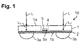
Fig. 1 shows a schematical illustration of a chip module 10. The chip module
10
may comprise a carrier 1 having a first main surface la, denoted hereinforth
as top
surface, and a second main surface lb, denoted hereinforth as bottom surface,
the bottom surface lb being opposite to the top surface la. The carrier 1 may
comprise an electrically isolating material. The carrier 1 may comprise for
example
a semiconductor material or alternatively a fibreglass reinforced epoxy
material,
such as FR4. It may be possible for the carrier 1 to comprise a flexible
circuit
material, such as for example polyester, polyimide, polyetherimide or
polyethylene
naphthalate. The chip module 10 may further comprise a metallization layer 2
being arranged on the bottom surface lb. The metallization layer 2 may be
deposited on the bottom surface lb of the carrier 1 by conventional depositing
means, for example by galvanic deposition, electroplating, physical vapour
deposition (PVD), chemical vapour deposition (CVD), sputtering or similar
deposition techniques. The metallization layer 2 may also be a metal sheet
bonded to the carrier 1. The metallization layer 2 may for example comprise a
copper layer or copper sheet. The metallization layer 2 may be coated with
silver
or gold in order to reduce oxidation effects on the surface of the
metallization layer
2.
The chip module 10 may further comprise a first recess structure 4, which is
arranged in the carrier 1 from the top surface la. The first recess structure
4 may
for example be arranged substantially in the centre portion of the chip module
10.
The first recess structure 4 may have any desired shape and size. In
particular,
CA 02843203 2014-01-27
WO 2013/026697
PCT/EP2012/065433
7
the first recess structure 4 may be dimensioned to house a chip 5 within the
first
recess structure 4. The chip 5 may for example be an RF1D chip. The chip 5 may
be arranged in the first recess structure 4. In one embodiment, the first
recess
structure 4 may be recessed into the carrier material to a predetermined depth
that
does not exceed the total depth of the carrier 1. In this case, the chip 5 may
be
directly adhered to the bottom of the first recess structure 4. In one
embodiment,
the first recess structure 4 may be arranged in the carrier material so as to
form a
throughhole through the carrier 1 In this case, the chip 5 may be coupled to
the
metallization layer 2 by means of an electrically isolating adhesive layer 5a.
The chip module 10 may further comprise electrically conductive connecting
material, in particular solder material, arranged on the metallization layer
2. The
electrically conductive connecting material may for example be deposited as
solder bumps 3a, 3b. In Fig. 1 two solder bumps 3a, 3b are exemplarily shown,
however, any other numbers of solder bumps are equally possible. The solder
bumps 3a, 3b may be arranged in edge portions of the chip module 10. In
particular, the solder bumps 3a, 3b may be arranged in an area of the chip
module
10 which is not situated below the centre portion, where the chip 5 is
arranged in
the first recess structure 4. It is also possible to use other connecting
material
instead of solder material, for example electrically conductive glue, which
may
form connection bumps similar to the solder bumps 3a, 3b.
In order to solder the chip module 10 to a substrate (not shown), laser beams
L
may be used to irradiate the chip module 10. The laser beams L may be directed
in a right or substantially right incidence angle towards the top surface la
of the
carrier 1. The energy of the laser beams L may be transferred through the main
body of the carrier 1 towards the metallization layer 2. The chip module 10
may be
irradiated at areas of the top surface la which lie directly opposite of the
area on
the bottom surface lb where the solder bumps 3a, 3b are deposited. In that
way,
the energy of the laser beams L is transferred through the carrier 1 and heats
up
the metallization layer 2 and the solder bumps 3a, 3b, thereby ref lowing the
solder
or connecting material. The reflown solder material may be used to solder the
chip
module 10 to a substrate below the solder bumps 3a, 3b.
Fig. 2A and 2B show schematical illustrations of the chip module 10 of Fig. 1
in
isometric view according to a further embodiment of the invention. Fig. 2A
shows
CA 02843203 2014-01-27
WO 2013/026697
PCT/EP2012/065433
8
an isometric view on the top surface la of the chip module 10, whereas Fig. 2B
shows an isometric view on the bottom surface la of the chip module 10.
The metallization layer 2 may be patterned to form first and second
metallization
structures 2a and 2b, as exemplarily depicted in Fig. 2B. The first and second
metallization structures 2a and 2b may be patterned to be electrically
isolated from
each other. The first and second metallization structures 2a and 2b may for
example be patterned with a continuous metallization member extending over an
edge portion of the chip module 10 on the bottom surface lb and with a
metallization land extending from the continuous metallization member towards
the centre portion of the chip module 10. The metallization lands of each of
the
first and second metallization structures 2a and 2b may be arranged on
opposite
sides of the chip module 10. It should be noted, that the shape and dimensions
of
the first and second metallization structures 2a and 2b in Fig. 2A and 2B are
only
exemplary, and that any other shape, size and structure of the first and
second
metallization structures 2a and 2b may equally be possible.
The chip 5 within the first recess structure 4 may be electrically connected
to the
first and second metallization structures 2a and 2b. The electrical connection
may
for example be established by wire bonds (not shown) extending from terminals
of
the chip 5 to each of the first and second metallization structures 2a and 2b.
For
example, a first wire bond may be connected to a first terminal of the chip 5
and to
a metallization land of the first metallization structures 2a. A second wire
bond
may be connected to a second terminal of the chip 5 and to a metallization
land of
the second metallization structures 2b.
An additional layer (not shown) may be provided between the metallization
layer 2
and the carrier 1. For example, a photoresist layer may be provided between
the
metallization layer 2 and the carrier 1. The carrier 1 may comprise a material
which is substantially transparent to visible, UV, and/or infrared light. In
particular,
the carrier 1 may comprise a material which has a high transmission
coefficient or
transmittance for laser beams L guided through the carrier 1. The laser beams
L
may be transmitted substantially without energy loss as laser beams LT through
the carrier 1. The photoresist layer may then comprise a material which has a
low
transmittance, that is, a high absorbance for the laser beams LT. Laser beams
L
that are used to irradiate the chip module 10 in order to perform a laser
reflow
soldering process for the solder bumps 3 are able to heat up the solder bumps
3
CA 02843203 2014-01-27
WO 2013/026697
PCT/EP2012/065433
9
more quickly, since most of the laser energy is transmitted through the
carrier 1
and deposited in the photoresist layer near the metallization layer 2 and the
solder
bumps 3.
Fig. 3 shows a schematical illustration of a chip module 20. The chip module
20
differs from the chip module 10 in that additional recess structures 6a, 6b
are
formed in the carrier 1. A second recess structure 6a is formed in an edge
portion
of the carrier 1 from the top surface la towards the bottom surface lb. A
third
recess structure 6b is formed in an edge portion of the carrier 1 opposite to
the
edge portion where the second recess structure 6a is formed from the top
surface
la towards the bottom surface lb. The recess structures 6a, 6b may be formed
to
a depth which is lower than the thickness of the carrier 1. Alternatively, the
recess
structures 6a, 6b may be formed as vias through the main body of the carrier
1,
that is, the vias extend through the whole thickness of the carrier 1. The
bottom of
the recess structures 6a, 6b may be coated with a photoresist in order to
increase
the absorbance of laser beams L guided through the recess structures 6a, 6b.
Fig. 4 shows a schematical illustration of a chip module 30. The chip module
30
differs from the chip module 20 in that the additional recess structures 6a,
6b are
formed as vias through the carrier 1 and through the metallization layer 2. In
other
words, the recess structures 6a, 6b extend from the top surface la of the
carrier 1
through the whole thickness of the carrier 1 and through the whole thickness
of the
metallization layer 2 to the bottom surface lb of the chip module 30. Solder
bumps
3a, 3b deposited on the metallization layer 2 may preferably be arranged on
the
bottom surface lb over the exits of the vias formed by the recess structures
6a,
6b, respectively.
The second and third recess structures 6a, 6b may have any shape and size. For
example, as schematically shown in Fig. 5, which shows an isometric view of
the
chip module 30 in Fig. 4, the second and third recess structures 6a, 6b may
have
a circular shape and are formed as cylindrical tubes extending through the
carrier
1 and/or the metallization layer 2.
Fig. 6 shows a schematical illustration of a manufacturing apparatus 40 for
connecting chip modules to a substrate 47. Exemplarily, a chip module 10 is
shown in Fig. 6, however, any other chip module 10, 20 or 30 as detailed
above,
may be used as well. The manufacturing apparatus 40 may comprise a laser
CA 02843203 2014-01-27
WO 2013/026697
PCT/EP2012/065433
device 41 having an active laser portion 41a, a stencilling device 42, a
stencilling
mask 45 and a base plate 46. The laser device 41 and the stencilling device 42
may be aligned with respect to each other by means of a guiding housing 43.
The
stencilling device 42 may comprise a stencil head 44. The stencil head 44 may
5 comprise a plurality of hollow structures 44a, through which laser beams
L from
the active laser portion 41a may be guided towards the chip module 10.
The chip modules 10 may be provided as a tape comprising a plurality of chip
modules 10 connected adjacently to each other. For example, the tape may
10 comprise a number of parallel rows of chip modules 10 and the tape may
be
guided through the stencilling mask 45 during the operation of the
manufacturing
apparatus 40.
The operation of the manufacturing apparatus will be explained in conjunction
with
the method 50 schematically illustrated in Fig. 7. The method 50 comprises in
a
first step 51 placing a chip module on a substrate 47. This may be done by
stencilling the chip module from a tape, the tape comprising a plurality of
chip
modules. Any of the chip modules 10, 20 or 30 a shown above in conjunction
with
Figs. 1 to 5 may be used in the method 50 of Fig. 7.
The chip module may be arranged in the stencilling mask 45 such that the
second
main surface lb of the chip module faces the substrate 47. The substrate 47
may
for example be a textile substrate 47 having a metallization structure
arranged
thereon. The metallization structure may for example be an RF1D antenna
structure. The stencilling head 44 may be brought down along the guiding
housing
43 in order to stencil the chip module 10 from the tape with chip modules 10.
The
chip module 10 cut out from the tape may be held against the stencilling head
44
by means of underpressure applied through a channel 42a within the stencilling
head 44.
The chip module 10 may in a second step 52 be aligned by aligning the first
solder
bump 3a and the second solder bump 3b of the chip module 10 with
corresponding first and second metallization patterns on the substrate 47. In
a
third step 53, the chip module 10 may be irradiated with laser beams L, the
laser
beams L being guided through the hollow structures 44a of the stencilling head
44
and thus hitting the first main surface la at a right or substantially right
incidence
angle. The laser device 41 may be controlled to apply one or more laser pulses
to
CA 02843203 2014-01-27
WO 2013/026697 PCT/EP2012/065433
11
the chip module 10, wherein the energy of the laser pulses is controlled to
ref lowing the first and the second solder bumps in a fourth step 54. Thereby
a
solder connection between the first and the second solder bumps 3a, 3b and the
corresponding first and second metallization patterns on the substrate 47 may
be
formed.
A system for connecting a chip module to a substrate, may comprise means for
placing the chip module on a substrate, the second main surface of the chip
module facing the substrate, means for aligning the first solder bump and the
second solder bump of the chip module with corresponding first and second
metallization patterns on the substrate, means for irradiating the chip module
with
laser beams, the laser beams hitting the first main surface at a right
incidence
angle, and means reflowing the first and the second solder bumps by the laser
beams, thereby forming a solder connection between the first and the second
s solder bumps and the corresponding first and second metallization
patterns on the
substrate.
Fig. 8 shows a schematical illustration of an RFID label 60 manufactured for
example by using a method 50 in a manufacturing apparatus 40 as shown in Fig.
6
and 7. The RFID label 60 is formed by a chip module 10, 20 or 30, as detailed
in
conjunction with Figs. 1 to 5, which is soldered to metallization patterns 62
on the
surface of a substrate 62. The substrate 62 may for example be the same
substrate as substrate 47, particularly a textile substrate. The metallization
patterns 62 may form an RFID antenna structure serving as an RFID antenna for
the RFID chip 5 arranged in the recess structure 4 of the carrier 1. The
soldering
connection is procured by the reflown soldering bumps 3a and 3b, respectively,
which are shown as substantially flat structures in Fig. 8.
Particular features of an embodiment of the invention may have been disclosed
with respect to only one of several implementations, however, said feature may
be
combined with one or more other features of the other implementations as may
be
desired and advantageous for any given or particular application. Furthermore,
to
the extent that the terms "include", "have", "with", or other variants thereof
are
used in either the detailed description or the claims, such terms are intended
to be
inclusive in a manner similar to the term "comprise". The terms 'coupled" and
"connected", along with derivatives may have been used. It should be
understood
that these terms may have been used to indicate that two components work
CA 02843203 2014-01-27
WO 2013/026697
PCT/EP2012/065433
12
together or interact with each other, irrespective of whether they are in
direct
physical or electrical contact or not. Additionally, any terminology used in
the
foregoing description related to the spatial arrangement of features, elements
or
components of the embodiments depicted in the drawings, such as "top",
"bottom",
"left", "right", "lower", "upper" and similar terms, is used solely for
purposes of an
easier understanding and is not intended to limit the invention in any way.