Note : Les descriptions sont présentées dans la langue officielle dans laquelle elles ont été soumises.
CA 02844698 2014-02-07
WO 2013/032840
PCT/US2012/052003
ELECTROMAGNETIC INTERFERENCE SHIELD
FIELD OF THE DISCLOSURE
[0001] The present disclosure relates to electromagnetic interference shields
for printed circuit boards.
BACKGROUND
[0002] Electronic circuitry assemblies, printed circuits boards (PCBs), and
substrates containing circuitry and electronic components mounted thereon,
often require electromagnetic interference (EMI) shields to limit the
likelihood of
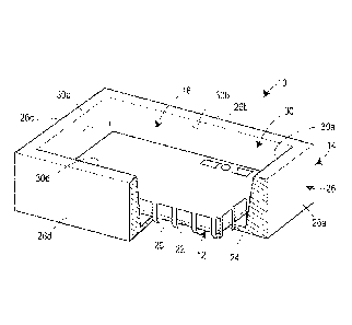
signal interferences from electromagnetic waves, such as those caused by
radio-frequency (RF) signals, high-power transmission lines, and other
electronic and/or industrial components, for example.
[0003] EMI shields are often installed over or in proximity to sensitive
electronic components on a circuit board to inhibit interference from
propagating. An EMI shield may be varying in shape and size in relation to the
sensitivity of the electronics and the material used in construction of the
EMI
shield. It is known that an EMI shield is typically comprised of a metal
sheet, a
casting, or other conductive material such as a mesh or paint which is formed
into a shape in relation to both the components and the space available on the
circuit board. An EMI shield is usually precisely placed on a circuit board at
a
prescribed location and is attempted to be grounded, usually with a circuit
ground. The EMI shield is typically installed by securing the shield to the
circuit
board. Often, compression fittings, screws, and/or soldering are used to
secure
the shield in place within an electronics enclosure or other housing, for
example.
SUMMARY
[0004] One of the present disclosure provides a device for protecting a
circuit board from electromagnetic interference, and which includes shield to
be
attached to the circuit board. The device includes a metal plate and a
plurality
1
CA 02844698 2014-02-07
WO 2013/032840
PCT/US2012/052003
of tangs. The metal plate has a perimeter portion. The plurality of tangs are
spaced about and extend transversely away from at least a portion of the
perimeter portion of the metal plate. Each tang includes a bridge portion and
a
finger portion. The bridge portion has a first end attached to the perimeter
portion and a second end spaced away from the perimeter portion and
attached to the finger portion. The finger portion extends away from the
second end of the bridge potion and is disposed at an obtuse angle relative to
the bridge portion such that the plurality of tangs, in combination, are
adapted
to receive the circuit board.
[0005] Another aspect of the present disclosure provides an assembly,
which includes a circuit board, an enclosure, and at least one metal shield.
The
circuit board has a perimeter edge. The enclosure has a bottom wall and at
least one sidewall disposed around a perimeter of the bottom wall. The
sidewall includes an inclined interior wall surface such that the enclosure
defines a cavity between the bottom wall and the at least one sidewall. The
cavity has a cross-sectional dimension that diverges away from the bottom
wall. The at least one metal shield is attached to the circuit board for
protecting
the printed circuit board from electromagnetic interference. The shield
includes
a metal plate having a perimeter portion and a plurality of tangs extending
away
from the perimeter portion. The circuit board and the shield are disposed in
the
cavity of the enclosure such that each of the tangs of the shield are disposed
between the perimeter edge of the circuit board and the at least one sidewall
of the enclosure such that the inclined interior wall surface of the at least
one
sidewall urges the tangs toward the perimeter edge of the circuit board.
[0006] Another aspect of the present disclosure provides a method of
manufacturing an electrical assembly. The method includes forming an
enclosure having a bottom wall and at least one sidewall with an inclined
interior surface, wherein the sidewall extends about and away from the bottom
wall to define a cavity between the bottom wall and the at least one sidewall.
The method further includes providing a circuit board. Moreover, the method
includes stamping a first metal shield comprising a first plate with a first
2
CA 02844698 2014-02-07
WO 2013/032840
PCT/US2012/052003
perimeter portion and a first plurality of tangs extending from the first
perimeter
portion. Furthermore, the method includes bending the first plurality of tangs
of
the first metal shield transverse to the first plate and positioning the
circuit
board between the first plurality of tangs of the first metal shield. The
method
also includes positioning the circuit board and first metal shield into the
cavity of
the enclosure such that the inclined interior surface of the at least one
sidewall
contacts the first plurality of tangs and urges the first plurality of tangs
toward a
perimeter edge of the circuit board.
BRIEF DESCRIPTION OF THE DRAWINGS
[0007] Fig. 1 is a perspective view of an electromagnetic interference
(EMI)
shield and printed circuit board (PCB) constructed and assembled in
accordance with the principles of the present disclosure.
[0008] Fig. 2 is a partial cut-away perspective view of the EMI shield and
PCB of Fig. 1 disposed within an enclosure and constructed and assembled in
accordance with the principles of the present disclosure.
[0009] Fig. 3 is a detailed sectional view taken from circle 3 of Fig. 2.
[0010] Fig. 4 is a detailed view of one version of a circuit board
constructed
in accordance with the principles of the present disclosure.
[0011] Fig. 5 is a cross-sectional side view of an EMI shield, PCB, and
enclosure constructed in accordance with one alternative version of the
present
disclosure.
DETAILED DESCRIPTION
[0012] The present disclosure is directed to an electromagnetic interference
(EMI) shield and related assembly including a printed circuit board (PCB) and
enclosure, which beneficially reduces manufacturing and assembly times and
ensures accurate alignment of the component parts.
3
CA 02844698 2014-02-07
WO 2013/032840
PCT/US2012/052003
[0013] For example, Fig. 2 depicts an assembly 10 constructed and
assembled in accordance with the principles of the present disclosure and
includes a circuit board 12 such as a PCB, an enclosure 14, and an EMI shield
16. The enclosure 14 in Fig. 2 includes a partially cut-away portion to
illustrate
the positional relationship of the component parts, as will be described. Fig.
1
depicts the circuit board 12 and EMI shield 16 removed from the enclosure 14.
In the disclosed version, the circuit board 12 comprises a generally
rectangular
circuit board 12 having a top surface 18, a bottom surface 20, and a perimeter
edge 22, as is also identified in Fig. 3.
[0014] The enclosure 14 can be a generally conventional enclosure formed
of plastic or metal casting, and includes a bottom wall 24 and at least one
sidewall 26. In the disclosed version, because the circuit board 12 is
generally
rectangular, the bottom wall 24 of the enclosure 14 is also rectangular. As
such, that at least one sidewall 26 of the disclosed version of the enclosure
14
includes first through fourth sidewalls 26a-26d. So configured, the sidewalls
26a-26d are disposed around a perimeter of the bottom wall 24 to define a
cavity 28 between the bottom wall 24 and the sidewalls 26a-26d of the
enclosure 14. Each of the sidewalls 26a-26d includes a corresponding inclined
interior wall surface 30a-30d. The interior wall surfaces 30a-30d of opposing
sidewalls 26a-26d diverge away from the bottom wall 24. More specifically, the
interior wall surfaces 30a, 30c of the first and third sidewalls 26a, 26c
diverge
away from each other as they extend away from the bottom wall 24. Similarly,
the interior wall surfaces 30b, 30d of the second and fourth sidewalls 26b,
26d
diverge away from each other as they extend away from the bottom wall 24.
[0015] While the circuit board 12 and correspondingly, the enclosure 14, of
the version of the assembly depicted in the figures are generally rectangular
in
shape, the disclosure is equally applicable and intended to include circuit
boards having generally any shape. The circuit board 12 could be circular,
square, triangular, hexagonal etc. In any of these cases, the shape and
configuration of the enclosure 14 and the EMI shield 16, which is to be
4
CA 02844698 2014-02-07
WO 2013/032840
PCT/US2012/052003
discussed in more detail below, would be correspondingly adjusted to
accommodate the differently shaped circuit board 12.
[0016] Referring again to Figs. 1 and 2, the EMI shield 16 is attached to
the
circuit board 12 for protecting the circuit board 12 from electromagnetic
interference. The EMI shield 16 includes a metal plate 32 having a perimeter
portion 34 and a plurality of tangs 36 extending away from the perimeter
portion
34. In a preferred version of the EMI shield 16, the metal plate 32 and the
tangs
36 are constructed from a single piece of metal and manufactured through a
stamping operation, for example.
[0017] In the disclosed version, the plurality of tangs 36 are spaced
generally
equally about the entirety of the perimeter portion 34 of the metal plate 32.
Preferably, the spacing between adjacent tangs is equal to or less than
approximately 1/2". Not all spacing must be equal to each other, however. In
some versions, however, the plurality of tangs 36 could only be spaced about a
portion of the perimeter portion 34, for example, along three of the four
sides.
Moreover, the plurality of tangs 26 extend transversely away from the metal
plate 32. Referring to Fig. 3 and for the sake of description, each tang 36 of
the
currently disclosed version includes a bridge portion 38 and a finger portion
40,
as identified in Fig. 3, wherein the bridge portion 38 is longer than the
finger
portion 40. The bridge portion 38 of each tang 36 includes a first end 38a
attached to the perimeter portion 34 of the plate 32 and a second end 38b
spaced away from the perimeter portion 34 and attached to the finger portion
40. The finger portion 40 extends away from the second end 38b of the bridge
potion 38 and is disposed at an angle relative to the bridge portion 38. In
the
disclosed version, the angle is an obtuse angle, i.e., the angle is great than
90 .
So configured, and as depicted in Fig. 3, each of the plurality of tangs 36
defines a recess 42 where the bridge portion 38 meets the finger portion 40.
The recesses 42 of the plurality of tangs 36, in combination, receive the
circuit
board 12 to attach the EMI shield 16 to the circuit board 12.
[0018] Referring to Figs. 2 and 3, the circuit board 12 and the EMI shield
16
are disposed in the cavity 28 of the enclosure 14 such that each of the tangs
36
CA 02844698 2014-02-07
WO 2013/032840
PCT/US2012/052003
of the EMI shield 16 are disposed between the perimeter edge 22 of the circuit
board 12 and the at least one sidewall 26a-26d of the enclosure 14. More
specifically, as shown in Fig. 3, each of the tangs 36 of the EMI shield 16
are
disposed between the perimeter edge 22 of the circuit board 12 and an inclined
interior surface 30a-30d of one of the sidewalls 26a-26d such that the
inclined
interior wall surfaces 30a-30d urge the tangs 36 toward the perimeter edge 22
of the circuit board 12. In the version depicted in Figs. 2 and 3, this urging
causes each of the tangs 36 to contact and become engaged with the
perimeter edge 22 of the circuit board 12. In the version depicted in Figs. 2
and
3, for example, this engagement between the tangs 36 and the perimeter edge
22 of the circuit board 12 creates a grounded electrical connection.
[0019] Specifically, as shown in Fig. 3, a metal ground plate 44 is mounted
to the bottom surface 20 of the circuit board 12 such that the ground plate 44
is
disposed between the circuit board 12 and the bottom wall 24 of the enclosure
14. In one form, the ground plate 44 can include a copper plate. While the
ground plate 44 is described as being attached to the circuit board 12, it
could
also be integrated into the circuit board 12 itself using a layer of copper,
for
example, on the board 12. To further facilitate the electrical connection
between the ground plate 44 and the tangs 36, the circuit board 12 includes a
plurality of notches 46, as shown in Fig. 4. Each of the notches 46 includes a
partially-cylindrical recess formed in the perimeter edge 22 of the circuit
board
12. An internal surface 48 of each notch 46 is further plated with solder or
some other electrically conductive material, for example, to provide an
electrically conductive surface on the perimeter edge 22, which is connected
directly to the ground plate 44.
[0020] Thus, when the EMI shield 16 depicted in Figs. 1-3 is attached to the
circuit board 12, each of the plurality of tangs 36 is disposed in one of the
notches 46 on the perimeter edge 22 and in contact with the plated surface 48
such that the EMI shield 16 is electrically connected to the ground plate 44,
thereby completing the electrical connection and enabling the complete system
6
CA 02844698 2014-02-07
WO 2013/032840
PCT/US2012/052003
to protect any components that might be mounted on the top surface 18 of the
circuit board 12 from the detrimental effects of electromagnetic interference.
[0021] While the EMI shield 16 depicted in FIGS. 1-3 is the same size as the
corresponding circuit board 12 such that the tangs 36 all contact and engage
the perimeter portion of the circuit board 12, other versions or variations of
the
circuit board 12 could be accommodated. For example, the circuit board 12
may be arranged such that only a portion, e.g., half, of the circuit board 12
requires an EMI shield 16. In such situations, the circuit board 12 could
include
a plurality of holes (not shown) arranged along a line, for example, through
the
center of the board 12 for receiving corresponding tangs 36 of an
appropriately
sized EMI shield 16. Similar to the notches 46 described with reference to
Fig.
4, the holes could also be plated to facilitate an electrical connection with
the
ground plate 44.
[0022] Further still, while the assembly 10 depicted in Figs. 1-3 has been
described as including a single EMI shield 16 mounted above the top surface
18 of the circuit board 12 for protecting electronic components mounted only
to
the top surface 18, for example, Fig. 5 depicts an embodiment of an assembly
100 constructed in accordance with the principles of the present disclosure
that
includes first and second EMI shields 116a, 116b, mounted adjacent to
opposing top and bottom surfaces 118, 120 of a circuit board 112, thereby
being capable of protecting sensitive electronic components mounted to both
the top 118 and the bottom surfaces 120.
[0023] In Fig. 5, the first and second EMI shields 116a, 116b are
substantially identical to the EMI shield 16 described above with reference to
Figs. 1-3 in that they each include a corresponding plate 132a, 132b and
plurality of tangs 136a, 136b. Additionally, the enclosure 114 is
substantially
identical to the enclosure 14 described above with respect to Figs. 2 and 3.
As
such, all of the additional details of the EMI shields 116a, 116b and the
enclosure 114 will not necessarily be repeated.
7
CA 02844698 2014-02-07
WO 2013/032840
PCT/US2012/052003
[0024] The circuit board 112 of the assembly 100 depicted in Fig. 5 is
generally similar to the circuit board 12 described above, except that it does
not
require the ground plate 44. Moreover, the notches 46 are optional for
alignment purposes, but it would not be necessary that the internal surfaces
48
of the notches 46 be plated. The ground plate 44 would not be included
because the bottom surface 120 of the circuit board 112 would include
electronic components attached thereto similar to the top surface 118.
Moreover, as will be described, the assembly 100 depicted in Fig. 5 does not
rely on a ground plate 44 to complete the electrical ground connection.
[0025] Specifically, as shown in Fig. 5, when assembled, each of the
plurality
of tangs 136a of the first EMI shield 116a are disposed between a perimeter
edge 122 of the circuit board 112 and a sidewall 126 of the enclosure 114 such
that an inclined interior wall surface 130 of the sidewall 126 urges each of
the
tangs 136a of the first EMI shield 116a toward the perimeter edge 122 of the
circuit board 112. Furthermore, each of the plurality of tangs 136b of the
second EMI shield 116b is disposed between the perimeter edge 122 of the
circuit board 12 and one of the tangs 136a of the first EMI shield 116a.
[0026] So configured, as the inclined interior wall surface 130 of the
sidewalls 126 of the enclosure 114 urge the tangs 136a of the first EMI shield
116a toward the perimeter edge 122 of the circuit board 112, the tangs 136a of
the first EMI shield 116a are urged into contact with the tangs 136b of the
second EMI shield 116b and the tangs 136b of the second EMI shield 116b are
urged into contact with the perimeter edge 122 of the circuit board 112. The
contacting tangs 136a, 136b creates an electrical connection between the first
and second EMI shields 116a, 116b. So configured, the first and second EMI
shields 116a, 116b of the assembly 100 depicted in Fig. 5 provide protection
above the top surface 118 and below the bottom surface 120 of the circuit
board 112.
[0027] In Fig. 5, the tangs 136b of the second EMI shield 116b are depicted
as being disposed between the tangs 136a of the first EMI shield 116a and the
perimeter edge 122 of the circuit board 112, but in an alternative version,
the
8
CA 02844698 2014-02-07
WO 2013/032840
PCT/US2012/052003
tangs 136a, 136b of the first and second EMI shields 116a, 116b could be
reversed.
[0028] Based on the foregoing description, it should be appreciated that
the
unique arrangement and configuration of the tangs 36, 136a, 136b extending
from the EMI shield(s) 16, 116a, 116b enable for a simple assembly of the EMI
shield(s) 16, 116a, 116b to the circuit board 12, 112, while the inclined
interior
wall surfaces 30, 130 of the disclosed enclosure 14, 114 helps to maintain the
desired electrical contact.
[0029] Additionally, in embodiments wherein the circuit boards 12, 112
include the notches 46 formed in the perimeter edge 22, 122, the present
disclosure further ensures that the EMI shields 16, 116a, 116b are properly
and
accurately aligned relative to the circuit boards 12, 112, which alignment can
affect the performance of the EMI shields 16, 116a, 116b in some applications.
In some versions, the EMI shield 16, 116a, 116b and the circuit board 12, 112
can finally be secured into the enclosure 14, 114 with ordinary means
including
fasteners, adhesive, potting, etc., if desired.
[0030] One method of manufacturing the assembly 10 depicted in Figs. 2
and 3 includes forming the enclosure 14 such that the enclosure 14 includes
the bottom wall 24 and the at least one sidewall 26 with inclined interior
surface
30. The enclosure 14 can be formed by molding plastic or casting metal, for
example. Additionally, the method includes providing the circuit board 12.
Furthermore, the method includes stamping the EMI shield 16 to include the
plate 32 with the first perimeter portion 34 and the plurality of tangs 36
extending from the perimeter portion 34. Furthermore, the method includes
bending the plurality of tangs 36 of the EMI shield 16 transverse to the plate
32.
To achieve the specific construct of the tangs 36 described above with
reference to Fig. 3, for example, the method further includes bending a distal
portion of each of the plurality of tangs 36 to include the bridge portion 38
attached to the perimeter portion 34 of the metal plate 32 and the finger
portion
40 extending from the bridge portion 38 to define the recess 42.
9
CA 02844698 2014-02-07
WO 2013/032840
PCT/US2012/052003
[0031] The circuit board 12 is then positioned between the plurality of
tangs
36 and into the recesses 42 of the tangs 36, and the circuit board 12 and EMI
shield 16 can be positioned into the cavity 28 of the enclosure 14. More
specifically, the circuit board 12 and EMI shield 16 are inserted into the
cavity
28 such that the inclined interior surface 30 of the sidewalls 26 contact the
tangs 26 and urges them toward the perimeter edge 22 of the circuit board 12.
In the version disclosed in reference to Figs. 2 and 3, the inclined interior
surfaces 30 of the sidewalls 26 urge the tangs 36 into direct abutting contact
with the perimeter edge 22 of the circuit board 12 and, as such, into
electrical
contact with the ground plate 44 mounted to the bottom surface 20 of the
circuit
board 12 via the plated internal surfaces 48 of the notches 46.
[0032] To manufacture the notches 46 in the perimeter edge of the circuit
board 12, one method further includes drilling a plurality of holes through a
circuit board blank. The circuit board blank is then cut along a line that
extends
through the plurality of holes to form the circuit board 12 having the
perimeter
edge 22, which is defined by the cut, having the plurality of notches 46.
Additionally, for the version of the assembly disclosed with reference to
Figs. 2
and 3, the interior surface 48 of the notches 46 are plated with solder, for
example. The surfaces 48 can be plated either before or after the circuit
board
blank is cut to form the circuit board 12.
[0033] With the circuit board 12 formed to include the notches 46, the EMI
shield 16 is attached to the circuit board 12 by positioning the circuit board
12
between the tangs 36 such that each tang 36 is positioned in a corresponding
notch 46. This facilitates easy assembly and ensures proper alignment of the
EMI shield 16 relative to the circuit board 12.
[0034] The assembly 100 described with reference to Fig. 5 can be
manufactured and assembled in generally the same manner as the assembly
described above, with the exception that that notches 46 are optional and
the assembly 100 includes the first and second EMI shield 116a, 116b.
Nonetheless, the first and second EMI shields 116a, 116b are each
manufactured identical to the EMI shield 16 described above. That is, the EMI
CA 02844698 2014-02-07
WO 2013/032840
PCT/US2012/052003
shields 116a, 116b are first stamped, and then the tangs 136a, 136b are bent,
as desired.
[0035] With the first and second EMI shields 116a, 116b formed, as desired,
the circuit board 112 is positioned between the tangs 136b of the second EMI
shield 116b, as shown in Fig. 5. Then, the circuit board 12, with the second
EMI shield 116b attached, is positioned between the tangs 136a of the first
EMI
shield 116a. These three components, i.e., the circuit board 112, the first
EMI
shield 116a, and the second EMI shield 116b, are then positioned into the
enclosure 114, as depicted in Fig. 5. As these components are inserted into
the enclosure 114, the inclined interior surfaces 130 of the sidewalls
126contact
the tangs 136a of the first EMI shield 116a and urges them into contact with a
corresponding one of the tangs 136b on the second EMI shield 116b.
Moreover, the urging created by the inclined interior surfaces 130 further
urges
the tangs 136b of the second EMI shield into engagement with the perimeter
edge 122 of the circuit board 112. The contact between the tangs 136a of the
first EMI shield 116a and the tangs 136b of the second EMI shield 116b form
an electrical connection between the first and second EMI shields 116a, 116b
that completes a ground circuit for protecting any components carried by the
top and bottom surfaces of the circuit board 112.
[0036] While the tangs 36, 136a, 136b of the various EMI shields 16, 116a,
116b described herein are described as including a bridge portion 38 and
finger
portion 40 disposed at an obtuse angle relative to each other, thereby
defining
the recess 42, this is merely one example. Other versions of the EMI shields
16, 116a, 116b may include tangs that are not bent at all, except relative to
the
plates 32, 132, or may include tangs that occupy a different bent
configuration.
[0037] In view of the foregoing, it should be appreciated that the present
invention is not intended to be limited to the specific examples described
herein
and depicted in the attached figured, but rather, is intended to be defined by
the
spirit and scope of the following claims, which can be further exemplified by
the
following "aspects" of the invention.
11
CA 02844698 2014-02-07
WO 2013/032840
PCT/US2012/052003
[0038] Aspect 1. A device for providing an electromagnetic interference
shield to be attached to a circuit board for protecting the circuit board from
electromagnetic interference, the device comprising: a metal plate having a
perimeter portion; and a plurality of tangs spaced about and extending
transversely away from at least a portion of the perimeter portion of the
metal
plate, each tang including a bridge portion and a finger portion, the bridge
portion having a first end attached to the perimeter portion and a second end
spaced away from the perimeter portion and attached to the finger portion, the
finger portion extending away from the second end of the bridge potion and
being disposed at an obtuse angle relative to the bridge portion such that the
plurality of tangs, in combination, are adapted to receive a circuit board.
[0039] Aspect 2. The device of aspect 1, wherein the bridge portion of each
tang is longer than the finger portion of each tang.
[0040] Aspect 3. The device of any one of the preceding aspects, wherein
the flat metal plate and the plurality of tangs are formed from a single piece
of
metal.
[0041] Aspect 4. The device of any one of the preceding aspects, wherein
the plurality of tangs are spaced equal to or less than 1/2" apart about the
perimeter portion of the metal plate.
[0042] Aspect 5. The device of any one of the preceding aspects, wherein
each tang defines a recess where the bridge portion meets the finger portion
for receiving an edge of a circuit board.
[0043] Aspect 6. An assembly, comprising: a circuit board having a
perimeter edge; an enclosure having a bottom wall and at least one sidewall
disposed around a perimeter of the bottom wall, the sidewall including an
inclined interior wall surface such that the enclosure defines a cavity
between
the bottom wall and the at least one sidewall, the cavity having a cross-
sectional dimension that diverges away from the bottom wall; and at least one
metal shield attached to the circuit board for protecting the printed circuit
board
from electromagnetic interference, the shield comprising a metal plate having
a
12
CA 02844698 2014-02-07
WO 2013/032840
PCT/US2012/052003
perimeter portion and a plurality of tangs extending away from the perimeter
portion, the circuit board and the shield disposed in the cavity of the
enclosure
such that each of the tangs of the shield are disposed between the perimeter
edge of the circuit board and the at least one sidewall of the enclosure such
that the inclined interior wall surface of the at least one sidewall urges the
tangs toward the perimeter edge of the circuit board.
[0044] Aspect 7. The assembly of aspect 6, wherein the plurality of tangs
are spaced equal to or less than 1/2" apart about and extend transversely away
from the perimeter portion of the metal plate.
[0045] Aspect 8. The assembly of any one of aspects 6 to 7, wherein each
tang includes a bridge portion and a finger portion, the bridge portion having
a
first end attached to the perimeter portion of the metal plate and a second
end
spaced away from the perimeter portion of the metal plate, the finger portion
attached to and extending away from the second end of the bridge potion and
being disposed at an obtuse angle relative to the bridge portion such that the
plurality of tangs, in combination, receive the circuit board.
[0046] Aspect 9. The assembly of any one of aspects 6 to 8, wherein each
tang defines a recess where the bridge portion meets the finger portion, the
recess receiving a portion of the edge of the circuit board.
[0047] Aspect 10. The assembly of any one of aspects 6 to 9, wherein the
bridge portion of each tang is longer than the finger portion of each tang.
[0048] Aspect 11. The assembly of any one of aspects 6 to 10, wherein the
metal plate and the plurality of tangs of the at least one shield are formed
from
a single piece of metal.
[0049] Aspect 12. The assembly of any one of aspects 6 to 11, further
comprising a metal ground plate mounted to a surface of the circuit board and
disposed between the circuit board and the bottom wall of the enclosure, and
wherein the metal plate of the shield is disposed opposite the circuit board
from
the metal ground plate such that each of the plurality of tangs are
electrically
connected to the copper plate.
13
CA 02844698 2014-02-07
WO 2013/032840
PCT/US2012/052003
[0050] Aspect 13. The assembly of any one of aspects 6 to 12, wherein the
perimeter edge of the circuit board includes a plurality of plated notches
corresponding to the plurality of tangs of the shield, each of the plurality
of
plated notches receiving one of the plurality of tangs.
[0051] Aspect 14. The assembly of any one of aspects 6 to 13, wherein the
at least one metal shield comprises a first metal shield mounted to the
circuit
board and a second metal shield mounted to the circuit board opposite the
circuit board from the first metal shield, the plurality of tangs of the first
metal
shield disposed between the perimeter edge of the circuit board and the at
least one sidewall of the enclosure such that the inclined interior wall
surface
of the at least one sidewall urges each of the tangs into contact with the
perimeter edge of the circuit board, and the plurality of tangs of the second
metal shield disposed between the perimeter edge of the circuit board and the
at least one sidewall of the enclosure such that the inclined interior wall
surface of the at least one sidewall urges each of the tangs into contact with
one of the tangs of the first metal shield, thereby creating an electrical
connection between the first and second metal shields.
[0052] Aspect 15. A method of manufacturing an electrical assembly, the
method comprising: forming an enclosure having a bottom wall and at least one
sidewall with an inclined interior surface, the sidewall extending about and
away from the bottom wall to define a cavity between the bottom wall and the
at
least one sidewall; providing a circuit board; stamping a first metal shield
comprising a first plate with a first perimeter portion and a first plurality
of tangs
extending from the first perimeter portion; bending the first plurality of
tangs of
the first metal shield transverse to the first plate; positioning the circuit
board
between the first plurality of tangs of the first metal shield; positioning
the circuit
board and first metal shield into the cavity of the enclosure such that the
inclined interior surface of the at least one sidewall contacts the first
plurality of
tangs and urges the first plurality of tangs toward a perimeter edge of the
circuit
board.
14
CA 02844698 2014-02-07
WO 2013/032840
PCT/US2012/052003
[0053] Aspect 16. The method of aspect 15, further comprising: drilling a
plurality of holes through a circuit board blank; cutting the circuit board
blank
through the plurality of holes to form the circuit board as having a perimeter
edge having a plurality of notches.
[0054] Aspect 17. The method of any one of aspects 15 to 16, wherein
positioning the circuit board between the first plurality of tangs comprises
positioning each of the first plurality of tangs into a corresponding notch.
[0055] Aspect 18. The method of any one of aspects 15 to 17, further
comprising bending a distal portion of each of the first plurality of tangs to
include a bridge portion attached to the perimeter portion of the first metal
plate
and a finger portion extending from the bridge portion at an obtuse angle
relative to the bridge portion thereby defining a recess where the bridge
portion
meets the finger portion, the recess for receiving the perimeter edge of the
circuit board.
[0056] Aspect 19. The method of any one of aspects 15 to 18, further
comprising: stamping a second metal shield comprising a second plate with a
second perimeter portion and a second plurality of tangs extending from the
second perimeter portion; bending the second tangs of the second metal shield
transverse to the second plate; positioning the circuit board between the
second plurality of tangs of the second metal shield, prior to inserting the
circuit
board and the first metal shield into the cavity of the enclosure; and
positioning
the circuit board, the first metal shield, and the second metal shield into
the
cavity of the enclosure such that the inclined interior surface of the at
least one
sidewall contacts the first plurality of tangs and urges each of the first
plurality
of tangs into contact a corresponding one of the second plurality of tangs,
thereby forming an electrical connection between the first and second metal
shields.
Aspect 20. The method of any one of aspects 15 to 19, further comprising
urging the second plurality of tangs into contact with a perimeter edge of the
circuit board.