Note : Les descriptions sont présentées dans la langue officielle dans laquelle elles ont été soumises.
CA 02848832 2014-04-01
L12-1835W01
IMAGE PROCESSOR WITH MULTI-CHANNEL INTERFACE BETWEEN
PREPROCESSING LAYER AND ONE OR MORE HIGHER LAYERS
Field
The field relates generally to image processing, and more particularly to
processing of
images such as depth maps and other types of depth images.
Background
Image processing is important in a wide variety of different applications, and
such
processing may involve multiple images of different types, including two-
dimensional (2D)
images and three-dimensional (3D) images. For example, a 3D image of a spatial
scene may be
generated using triangulation based on multiple 2D images captured by
respective cameras
arranged such that each camera has a different view of the scene.
Alternatively, a 3D image can
be generated directly using a depth imager such as a structured light (SL)
camera or a time of
flight (ToF) camera. Multiple images of these and other types may be processed
in machine
vision applications such as gesture recognition, feature extraction, pattern
identification, face
detection, object recognition and person or object tracking.
In typical conventional arrangements, raw image data from an image sensor is
usually
subject to various preprocessing operations. Such preprocessing operations may
include, for
example, contrast enhancement, histogram equalization, noise reduction, edge
highlighting and
coordinate space transformation, among many others. The preprocessed image
data is then
subject to additional processing needed to implement one or more of the above-
noted machine
vision applications.
Summary
In one embodiment, an image processor comprises image processing circuitry
implementing a plurality of processing layers including a preprocessing layer
for received
image data and one or more higher processing layers coupled to the
preprocessing layer. The
image processor further comprises a multi-channel interface including at least
first and second
image data channels arranged in parallel with one another between the
preprocessing layer and
a given higher processing layer. The first image data channel is configured to
carry partial
depth information derived from the received image data to the given higher
processing layer,
and the second image data channel is configured to carry complete preprocessed
frames of the
received image data from the preprocessing layer to the given higher
processing layer.
1
CA 02848832 2014-04-01
L12-1835W01
By way of example only, in a given embodiment the partial depth information
comprises depth information determined to have at least a specified level of
reliability. Also,
the one or more higher processing layers coupled to the preprocessing layer
may comprise a
second processing layer coupled to a third processing layer, with the first
and second image
data channels being arranged in parallel with one another between the
preprocessing layer and
the third processing layer.
Other embodiments of the invention include but are not limited to methods,
apparatus,
systems, processing devices, integrated circuits, and computer-readable
storage media having
computer program code embodied therein.
Brief Description of the Drawings
FIG. 1 is a block diagram of an image processing system comprising an image
processor
having a preprocessing layer with a multi-channel interface to one or more
higher processing
layers in one embodiment.
FIGS. 2 and 3 illustrate progressively more detailed views of exemplary
processing
layers of the image processor of FIG. 1.
FIG. 4 shows another embodiment of an image processing system comprising an
image
processor implemented in the form of a controller chip having a preprocessing
layer and second
and third higher processing layers.
Detailed Description
Embodiments of the invention will be illustrated herein in conjunction with
exemplary
image processing systems that include image processors or other types of
processing devices
that implement a multi-channel interface between a preprocessing layer and one
or more higher
processing layers. It should be understood, however, that embodiments of the
invention are
more generally applicable to any image processing system or associated device
or technique
that can benefit from more efficient interaction between a preprocessing layer
and one or more
higher processing layers.
FIG. 1 shows an image processing system 100 in an embodiment of the invention.
The
image processing system 100 comprises an image processor 102 that receives
images from one
or more image sources 105 and provides processed images to one or more image
destinations
107. The image processor 102 also communicates over a network 104 with a
plurality of
processing devices 106.
=
2
CA 02848832 2014-04-01
L12-1835W01
Although the image source(s) 105 and image destination(s) 107 are shown as
being
separate from the processing devices 106 in FIG. 1, at least a subset of such
sources and
destinations may be implemented as least in part utilizing one or more of the
processing devices
106. Accordingly, images may be provided to the image processor 102 over
network 104 for
processing from one or more of the processing devices 106. Similarly,
processed images may
be delivered by the image processor 102 over network 104 to one or more of the
processing
devices 106. Such processing devices may therefore be viewed as examples of
image sources
or image destinations.
A given image source may comprise, for example, a 3D imager such as an SL
camera or
a ToF camera configured to generate depth images, or a 2D imager configured to
generate
grayscale images, color images, infrared images or other types of 2D images.
It is also possible
that a single imager or other image source can provide both a depth image and
a corresponding
2D image such as a grayscale image, a color image or an infrared image. For
example, certain
types of existing 3D cameras are able to produce a depth map of a given scene
as well as a 2D
image of the same scene. Alternatively, a 3D imager providing a depth map of a
given scene
can be arranged in proximity to a separate high-resolution video camera or
other 2D imager
providing a 2D image of substantially the same scene.
It is also to be appreciated that a given image source as that term is broadly
used herein
may represent an image sensor portion of an imager that incorporates at least
a portion of the
image processor 102. For example, at least one of the one or more image
sources 105 may
comprise a depth sensor, with the depth sensor being part of an SL camera, a
ToF camera or
other depth imager that incorporates the image processor 102. Numerous
alternative
arrangements are possible. For example, another example of an image source is
a storage
device or server that provides images to the image processor 102 for
processing.
A given image destination may comprise, for example, one or more display
screens of a
human-machine interface of a computer or mobile phone, or at least one storage
device or
server that receives processed images from the image processor 102.
Accordingly, although the image source(s) 105 and image destination(s) 107 are
shown
as being separate from the image processor 102 in FIG. 1, the image processor
102 may be at
least partially combined with at least a subset of the one or more image
sources and the one or
more image destinations on a common processing device. Thus, for example, a
given image
source and the image processor 102 may be collectively implemented on the same
processing
device. Similarly, a given image destination and the image processor 102 may
be collectively
implemented on the same processing device.
3
CA 02848832 2014-04-01
L12-1835W01
In the present embodiment, the image processor 102 comprises a preprocessing
layer
110-1 coupled to multiple higher processing layers denoted 110-2, 110-3 and so
on. The
preprocessing layer 110-1 and the higher processing layers such as layers 110-
2 and 110-3 are
collectively referred to herein as processing layers 110. Also, preprocessing
layer 110-1 is
referred to as Layer 1, and the higher processing layers denoted as respective
second and third
layers 110-2 and 110-3 are referred to as Layer 2 and Layer 3, respectively.
It will be assumed
for purposes of the further description to be provided below in conjunction
with FIGS. 2 and 3
that the higher processing layers of the image processor 102 comprise only the
processing
layers 110-2 and 110-3, with it being understood that more than three
processing layers 110
may be provided in the image processor 102 in other embodiments. The term
"higher" as used
in the context of processing layers herein should be understood to encompass
any processing
layers that receive outputs from a preprocessing layer and thus perform
subsequent processing
operations of those outputs.
The preprocessing layer 110-1 performs preprocessing operations on received
image
data from the one or more image sources 105. This received image data in the
present
embodiment is assumed to comprise raw image data received from a depth sensor,
but other
types of received image data may be processed in other embodiments.
The image processor 102 further comprises a multi-channel interface comprising
at least
first and second image data channels 111 and 112 arranged in parallel with one
another between
the preprocessing layer 110-1 and a given one of the higher processing layers
110-2 and 110-3.
The first image data channel 111 is configured to carry reliable partial depth
information
derived from the received image data to the given higher processing layer, and
the second
image data channel 112 is configured to carry complete preprocessed frames of
the received
image data from the preprocessing layer 110-1 to the given higher processing
layer. The partial
depth information may comprise, for example, depth information determined in
the
preprocessing layer 110-Ito have at least a specified level of reliability,
although other types of
partial depth information may be used in other embodiments. The first and
second image data
channels are also denoted herein as Channel 1 and Channel 2, respectively, or
as CH1 and CH2
in this particular figure.
The term "complete" as used herein in the context of a given preprocessed
frame sent
over the second image data channel 112 is intended to be broadly construed,
and should not be
construed as limited to any particular frame arrangement. For example, a
variety of different
preprocessed frames of different types may be sent over this channel. A given
complete
preprocessed frame may comprise, for example, a substantially full set of
depth information of
4
CA 02848832 2014-04-01
L12-1835W01
a depth image as preprocessed by the preprocessing layer 110-1, as contrasted
to partial depth
information sent over the first image data channel 111.
The particular number of image data channels of the multi-channel interface
between
the preprocessing layer 110-1 and the given higher processing layer can be
varied in other
embodiments. Accordingly, the multi-channel interface may comprise more than
two image
data channels arranged in parallel with one another in other embodiments.
As is illustrated in FIGS. 2 and 3, the first and second image data channels
111 and 112
are more particularly arranged in parallel with one another between the
preprocessing layer
110-1 and the third processing layer 110-3. However, in other embodiments, a
multi-channel
interface comprising a plurality of parallel image data channels may be
arranged between the
preprocessing layer 110-1 and additional or alternative higher processing
layers. The
preprocessing layer 110-1 further includes an interface 114 with a higher
processing layer other
than the one which is coupled via the multi-channel interface 111 and 112. In
this embodiment,
as will be illustrated in FIGS. 2 and 3, the interface 114 is assumed to be an
interface with the
second processing layer 110-2. It should be noted in this regard that one or
more interface
signal lines that are illustrated in the figures as bidirectional may
alternatively be unidirectional,
and vice versa.
The processing layers 110 may comprise different portions of image processing
circuitry
of the image processor 102, although a given such processing layer may be
implemented as a
combination of hardware, firmware and software. The term "layer" as utilized
herein is
therefore intended to be broadly construed, and may comprise, for example,
specialized
hardware, processing cores, firmware engines and associated firmware, or
general-purpose
processing resources and associated software executing on those resources, as
well as various
combinations of these and other types of image processing circuitry.
An otherwise conventional image processing integrated circuit or other type of
image
processing circuitry may be suitably modified to implement at least a portion
of one or more of
the processing layers 110 of image processor 102, as will be appreciated by
those skilled in the
art. One possible example of image processing circuitry that may be used in
one or more
embodiments of the invention is an otherwise conventional graphics processor
suitably
reconfigured to perform functionality associated with one or more of the
processing layers 110.
A more detailed example of an image processing circuitry arrangement of this
type in which the
graphics processor comprises a controller integrated circuit of an image
processing system will
be described in detail in conjunction with FIG. 4.
5
CA 02848832 2014-04-01
L12-1835W01
The processing devices 106 may comprise, for example, computers, mobile
phones,
servers or storage devices, in any combination. One or more such devices also
may include, for
example, display screens or other user interfaces that are utilized to present
images generated by
the image processor 102. The processing devices 106 may therefore comprise a
wide variety of
different destination devices that are configured to receive processed image
streams or other
types of output information from the image processor 102 over the network 104,
including by
way of example at least one server or storage device that receives such output
information from
the image processor 102.
Although shown as being separate from the processing devices 106 in the
present
embodiment, the image processor 102 may be at least partially combined with
one or more of
the processing devices 106. Thus, for example, the image processor 102 may be
implemented
at least in part using a given one of the processing devices 106. By way of
example, a computer
or mobile phone may be configured to incorporate the image processor 102 and
possibly a
given image source. The image source(s) 105 may therefore comprise cameras or
other imagers
associated with a computer, mobile phone or other processing device. As
indicated previously,
the image processor 102 may be at least partially combined with one or more
image sources or
image destinations on a common processing device.
The image processor 102 in the present embodiment is assumed to be implemented
using at least one processing device and comprises a processor 120 coupled to
a memory 122.
The processor 120 executes software code stored in the memory 122 in order to
control the
performance of image processing operations. The image processor 102 also
comprises a
network interface 124 that supports communication over network 104.
The processor 120 may comprise, for example, a microprocessor, an application-
specific
integrated circuit (ASIC), a field-programmable gate array (FPGA), a central
processing unit
(CPU), an arithmetic logic unit (ALU), a digital signal processor (DSP), or
other similar
processing device component, as well as other types and arrangements of image
processing
circuitry, in any combination.
The memory 122 stores software code for execution by the processor 120 in
implementing portions of the functionality of image processor 102, such as
portions of the
preprocessing layer 110-1 and the higher processing layers 110-2 and 110-3. A
given such
memory that stores software code for execution by a corresponding processor is
an example of
what is more generally referred to herein as a computer-readable medium or
other type of
computer program product having computer program code embodied therein, and
may
comprise, for example, electronic memory such as random access memory (RAM) or
read-only
6
CA 02848832 2014-04-01
L12-1835W01
memory (ROM), magnetic memory, optical memory, or other types of storage
devices in any
combination. As indicated above, the processor may comprise portions or
combinations of a
microprocessor, ASIC, FPGA, CPU, ALU, DSP or other image processing circuitry.
It should be apparent from the foregoing description that embodiments of the
invention
may be implemented in the form of integrated circuits. In a given such
integrated circuit
implementation, identical die are typically formed in a repeated pattern on a
surface of a
semiconductor wafer. Each die includes an image processor or other image
processing circuitry
as described herein, and may include other structures or circuits. The
individual die are cut or
diced from the wafer, then packaged as an integrated circuit. One skilled in
the art would know
how to dice wafers and package die to produce integrated circuits. Integrated
circuits so
manufactured are considered embodiments of the invention.
The particular configuration of image processing system 100 as shown in FIG. 1
is
exemplary only, and the system 100 in other embodiments may include other
elements in
addition to or in place of those specifically shown, including one or more
elements of a type
commonly found in a conventional implementation of such a system.
For example, in some embodiments, the image processing system 100 is
implemented as
a video gaming system or other type of gesture-based system that processes
image streams in
order to recognize user gestures. The disclosed techniques can be similarly
adapted for use in a
wide variety of other systems requiring a gesture-based human-machine
interface, and can also
be applied to applications other than gesture recognition, such as machine
vision systems in
robotics and other industrial applications.
The operation of the image processor 102 will now be described in greater
detail in
conjunction with the diagrams of FIGS. 2 and 3.
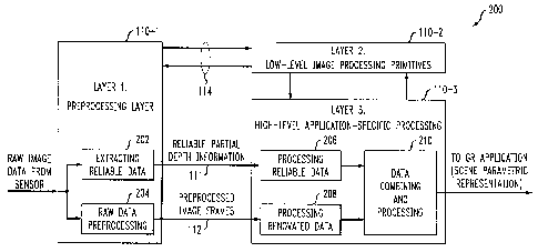
Referring initially to FIG. 2, a portion 200 of the image processor 102
comprises
preprocessing layer 110-1 and second and third higher processing layers 110-2
and 110-3, also
referred to as Layer 1, Layer 2 and Layer 3, respectively. The preprocessing
layer 110-1 is
coupled to the third processing layer 110-3 via first and second image data
channels 111 and
112, which are arranged in parallel with one another and carry reliable
partial depth information
and preprocessed image frames, respectively.
The preprocessing layer 110-1 is also coupled to the second processing layer
110-2 via a
bidirectional interface 114. In addition, the second processing layer 110-2
interacts with the
third processing layer 110-3 as indicated.
The preprocessing layer 110-1 in this embodiment comprises a data extraction
module
202 configured to separate the reliable partial depth information from other
depth information
7
CA 02848832 2014-04-01
L12-1835W01
of received raw image data, and a raw data preprocessing module 204 configured
to generate
the complete preprocessed frames. These modules have respective inputs coupled
to a source
of the received raw image data, which is assumed in this embodiment to
comprise a sensor of a
depth imager, and respective outputs coupled via the respective first and
second data channels
111 and 112 to the third processing layer 110-3.
The raw image data from the sensor may include a stream of frames comprising
respective depth images, with each such depth image comprising a plurality of
depth image
pixels. For example, a given depth image D may be provided to the
preprocessing layer 110-1
in a form of matrix of real values. Each such real value may more particularly
provide a depth
value du for a particular pixel of the depth image, where i and j denote pixel
indices, and the
depth value represents distance to an imaged object. A given such depth image
is also referred
to herein as a depth map.
A given pixel with indexes i, j and a depth value du can be transformed to
(x,y,z)
coordinates in 3D space. Also, if the depth is unknown for a given pixel, a
predefined value u
(e.g., zero) may be used as the depth value for that pixel. A wide variety of
other types of image
data may be used in other embodiments.
In some embodiments, a sensor that generates the depth values for the pixels
may also
provide corresponding reliability values for those pixels. For example, each
pixel (i, j)
supplied by a sensor of that type may comprise a pair (dy, ) where 0
:Clis a depth image
pixel reliability indicator or other type of reliability value. Alternatively,
the reliability values
may be estimated or otherwise determined in the preprocessing layer 110-1
based on known
characteristics of the particular type of sensor. The reliability values may
be part of a separate
reliability matrix, as will be described below in conjunction with FIG. 3.
Numerous other
techniques may be used to provide indications of the reliability associated
with particular pixels
or other portions of a depth image. Such determinations may be carried out at
least in part
within the preprocessing layer 110-1, or in other system elements.
The second processing layer 110-2 in this embodiment implements a plurality of
low-
level image processing primitives, particular examples of which will be
described in greater
detail below in conjunction with FIG 3. It should also be noted that such low-
level image
processing primitives may comprise one or more hardware-accelerated
recognition primitives
selected from a primitives library associated with the second processing
layer, as in the
embodiment of FIG. 4.
8
CA 02848832 2014-04-01
L12-1835W01
The third processing layer 110-3 in this embodiment implements high-level
application-
specific image processing, which is assumed to comprise at least gesture
recognition (GR), but
could additionally or alternatively comprise other types of high-level
application-specific image
processing such as activity recognition, emotion recognition and gaze
tracking. The third
processing layer 110-3 more particularly comprises a first processing module
206 adapted to
receive the reliable partial depth information carried over the first image
data channel 111, and
a second processing module 208 adapted to receive coupled the complete
preprocessed frames
carried over the second image data channel 112. The first and second
processing modules 206
and 208 are more particularly comprise respective reliable data processing and
renovated data
processing modules, the operation of which will be described in greater detail
in conjunction
with FIG. 3.
A data combining and processing module 210 is coupled to the first and second
processing modules 206 and 208 and configured to combine at least portions of
the partial depth
information and the complete preprocessed frames for subsequent processing. In
this
embodiment, the subsequent processing, which may be implemented in additional
higher
processing layers of the image processor 102 or in another processing device,
comprises at least
one GR application that utilizes GR output of the third processing layer 110-3
in the form of a
parametric representation of an imaged scene. Other types of processed image
data outputs
may be provided to one or more application layers of the image processor 102
or a related
processing device 106 or destination 107.
With reference now to FIG. 3, the portion 200 of the image processor 102 is
illustrated
in greater detail. This figure also shows preprocessing layer 110-1 coupled to
second and third
processing layers 110-2 and 110-3, including modules 202 and 204 of the
preprocessing layer
110-1 and modules 206, 208 and 210 of the third processing layer 110-3. Again,
the layers
110-1, 110-2 and 110-3 are more particularly denoted as Layer 1, Layer 2 and
Layer 3. The
modules 202, 204, 206 and 208 of Layer 1 and Layer 2 are also denoted as
processing blocks
1.1, 1.2, 3.1 and 3.2, respectively.
The processing block 3.1 is configured for processing reliable data received
from the
processing block 1.1 of preprocessing layer 110-1 via the first image data
channel 111, denoted
Channel 1 in this figure. In this embodiment, processing block 3.1 includes
block 3.1.1 in
which objects are detected based on models, and block 3.1.2 in which scenes
are segmented,
both of which may be implemented using well-known conventional techniques.
The processing block 3.2 is configured for processing renovated data received
from the
processing block 1.2 of preprocessing layer 110-1 via the second image data
channel 112,
9
CA 02848832 2014-04-01
L12-1835W01
denoted Channel 2 in the figure. In this embodiment, processing block 3.2
includes block 3.2.1
in which object geometric parameters such as center of mass are determined,
and block 3.2.2 in
which object edges and size are determined, again both of which may be
implemented using
well-known conventional techniques.
The data combining and processing module 210 is more particularly shown in
FIG. 3 as
comprising separate data combining and processing modules 210A and 2108,
denoted as
processing blocks 3.3 and 3.4, respectively.
In addition to blocks 1.1 and 1.2, the preprocessing layer 110-1 in this
embodiment
comprises processing blocks 1.3, 1.4, 1.5 and 1.6, configured for estimating
pixel reliability,
detecting edges, detecting reflections, and performing inter-frame
registration, respectively.
The various processing blocks of the processing layer 110-1 in the present
embodiment will
now be described in greater detail,
1.1 Extract reliable data
This block receives raw image data comprising a depth image D and extracts
highly
reliable depth information using additional information provided by blocks
1.3, 1.4 and 1.5.
The resulting reliable partial depth information is carried over Channel 1 of
the multi-channel
interface to processing layer 110-3,
1.1.1 Exclude pixels with low reliability
This block receives depth image D and a corresponding reliability matrix R
from
block 1.3, and generates a first modified depth image D' I
in which each pixel has either a
reliable depth value or an unknown depth value. For example, the pixels of the
first modified
depth image may be computed as follows:
du ry reliability _threshold
u otherwise
where u is a particular predetermined value indicative of unknown depth, such
as a
value of zero.
1.1.2 Exclude pixels near edges of close objects
CA 02848832 2014-04-01
,
L12-1835W01
This block receives the first modified depth image D' and a corresponding edge
matrix
E from block 1.4, and generates a second modified depth image D" dcill which
excludes
pixels near edges of close objects. For example, the pixels of the second
modified depth image
may be computed as follows:
{
d,.,... d,i' f (E,i, j) __closeness _threshold
' u otherwise
where u is again the above-noted predetermined value indicative of unknown
depth and
f (E,i, j) is a function that provides a value of closeness for one or more
objects in an area
surrounding the pixel (1, j) .
1.1.3 Exclude pixels related to reflections
This block receives the second modified depth image D" and a corresponding
reflection
matrix M from block 1.5, and generates a third modified depth image D" = kill
which
further excludes pixels related to reflections. For example, the pixels of the
third modified
depth image may be computed as follows:
dr' m, J =0
d,,,,, { J
j
where u is again the above-noted predetermined value indicative of unknown
depth,
and where my > 0 if the pixel (i, j) belongs to an area treated as a
reflection, and has a value of
zero otherwise. The third modified depth image in this embodiment represents
the reliable
partial depth information that is transmitted over Channel 1 of the multi-
channel interface to the
third processing layer 110-3. Other types of reliable partial depth
information may be used in
other embodiments. For example, only a subset of blocks 1.1.1, 1.1.2 and
1.1.3, such as only a
particular one of these blocks, may be utilized in other embodiments. A wide
variety of
alternative techniques may be used to identify reliable depth information from
a given depth
image. The term "partial depth information" as used herein is therefore
intended to be broadly
construed.
11
CA 02848832 2014-04-01
L12-1835W01
1.2 Raw data preprocessing
This block receives raw image data comprising depth image D and preprocesses
the
depth image to provide a corresponding preprocessed image frame using
additional information
provided by blocks 1.3, 1.4, 1.5 and 1.6. The resulting complete preprocessed
image frame is
carried over Channel 2 of the multi-channel interface to processing layer 110-
3.
1.2.1 Remove defects in depth image based on intraframe information
This block receives depth image D and generates depth image /5 from which
defects
have been removed utilizing intraframe information such as reliability matrix
R from block
1.3, edge matrix E from block 1.4, and reflection matrix M from block 1.5.
Objects which are
observed in the depth image D typically have surfaces, i.e., areas in which
neighboring pixels
have closely similar depth values: Idy ¨ diajl< h and Idy ¨ j+il< h for any i,
j in some area
A where h denotes a defect detection threshold. There are various types of
defects in such
surfaces which may result from noise and other technical or physical
characteristics of the
sensor. The threshold h is typically specified as larger than a depth
difference that would
ordinarily be produced by noise alone. Block 1.2.1 is configured to detect
defects that cause
depth differences that exceed the specified threshold h.
By way of example, a given defect may be defined as a "hole" in a surface, or
more
particularly as a limited area in which depth values differ significantly from
depth values of
surrounding areas, where the depth value difference across the boundary of the
area is abrupt
and opposite sides of the area have similar depth values.
An exemplary process will now be described for locating and removing at least
part of a
hole in a surface of the depth image. This process operates using only a
single row of depth
image pixels at a time, but may additionally or alternatively be implemented,
for example, using
a single column of depth image pixels at a time, or using single lines of
diagonal depth image
pixels at a time. Combinations of such arrangements may be used in order to
enhance the
quality of the defect removal process.
The process to be described utilizes an edge matrix E which in this context
more
particularly comprises a list of elements ek =(ik,jk,dk,ck) where ik, /lc, di,
denote indexed
position and depth value of a corresponding pixel k, and ck denotes the
direction of depth
change for that pixel. These elements of the list E are also referred to below
as candidate
border pixels.
12
CA 02848832 2014-04-01
L12-1835W01
The defect detection threshold h in this process more particularly specifies a
minimum
depth to the bottom of a hole. Other input parameters for the exemplary
process include the
following:
hole _size - maximum size hole that is considered removable;
border _dist _diff - maximum depth difference on opposite sides of a hole; and
border _dist _change - maximum depth change per pixel.
The process includes the following steps 1 through 3:
1. Fill in the list E of candidate border pixels using the rules given below.
This part of
the process is assumed to be performed in the edge detection block 1.4. The
particular rules
used to select depth image pixels as candidate border pixels may vary
depending on factors
such as input data quality and required selectivity. In the present
embodiment, the following
two candidate border pixel selection rules are utilized:
If a pixel (i, j) is such that d1.j+1¨ h
then it is a candidate border pixel of a left
border. Do the following: set ik = 1, jk = j,dk=c1ti and ck = 0, add
ek=(ik,jk,dk,ck) to the list
E, increment k.
If a pixel (i, j) is such that then
it is a candidate border pixel of a right
border. Do the following: set ik = , jk = j,dk= clv and ck =1, add ek
=(ik,jodk,ck) to the list
E, increment k.
2. Filter out left and right border pairs from the list E that satisfy the
constraints of hole
definition. As noted above, ek =(ik, jk,dock) is element k of the list E. In
the present
embodiment, it is assumed that a pair (ek,ek,i) of two subsequent elements
from E forms a
border pair of a hole in the row i if the following constraints are satisfied:
(a) The elements are the left and the right border: ck = 0 and ck+, ¨1;
(b) The elements are from the row i: ik = k+,;
(c) The hole has limited size: jkfl ¨ jk < hole _size;
(d) The opposite sides of the hole have similar depth:dk~l¨ dki < border _dist
_diff ;
and
(e) A difference between the depth of the opposite sides of the hole satisfy:
dk I
< border _dist _change
4+1 ik
13
CA 02848832 2014-04-01
L12-I 835W01
If all the constraints (a) through (e) are satisfied for the pair (eoek,i),
the next step of
the process is performed.
3. Repair the hole by filling the gap between the two border pixels selected
in step 2.
This may involve, for example, any of a number of different types of
interpolation. As a more
particular example, the following linear interpolation may be used:
a dk+1 - dk
4+1- Jk
b dk
= a=j+ b
where j takes on values from jk to jk+land row index i is fixed.
As indicated previously, the exemplary process described above removes defects
one
row at a time. It can be modified in a straightforward manner to remove
defects one column at
a time, or one diagonal line at a time, or using combinations of row, column
and line-based
implementations. Such arrangements can remove a large variety of different
types of depth
image defects.
As one example of a combined approach utilizing both rows and columns, let V
denote
a result of application of the process to rows of the depth image D , let W
denote a result of
application of the process to columns of the depth image D, and let v1 , Iv,
denote elements of
the corresponding matrixes.
The combined result b comprising elements a, may be determined from V and W in
different ways, such as using a minimal distance selection approach in which
au = min(vy, Ivo),
or using an averaging approach in which ay = (vy + .
The minimal distance selection
approach has been found to achieve better results than the averaging approach
in certain typical
applications.
In other embodiments, the exemplary process described above can be modified to
classify defects in other ways, such as by depth change direction and by
border type. For
example, classification by depth change direction may use holes and peaks, and
classification
by border type may use bounded holes and unbounded holes. The classification
by depth
change direction can be implemented by changing holes to peaks and back by
altering the
14
CA 02848832 2014-04-01
L12-1835W01
direction of the depth axis d: au¨do. The classification by border type allows
for the
identification of gaps that are completely surrounded by pixels classified as
border pixels as
well as other gaps that are not completely surrounded by pixels classified as
border pixels.
It should be noted that the process parameters should be selected to ensure
that natural
gaps within imaged objects are not inadvertently removed as defects. For
example, such natural
gaps are often observed between fingers of a hand. To avoid inadvertent
removal of these and
other natural gaps in the depth image, the process parameters may be adjusted
at least in part
based on feedback from higher processing layers.
As one example of such feedback, the third processing layer 110-3 may be
configured to
identify to the preprocessing block 110-1 one or more areas of the depth image
that contain
particular types of detected objects, such as hands, that are known to include
natural gaps. A
given such area, which could be identified using a bounding rectangle or other
shape, could
then be excluded from the defect removal process, or could be processed using
a different set of
parameters than other areas of the image.
The exemplary process for defect removal based on intraframe information
described
above is simple, and can be performed in parallel on multiple rows, columns or
other lines of
pixels of the depth image. However, in other embodiments alternative
techniques can be used
to remove defects based on intraframe information.
1.2.2 Remove defects in depth map based on interframe information
This block receives multiple processed depth images b from which defects have
been
removed based on intraframe information, and generates a modified depth image
D from
which additional defects are removed based on interframe information. For
example, it may
utilize first and second processed depth images D, and A , where A is a
processed depth
image corresponding to a current frame and h, is a processed depth image
corresponding to a
past frame, such as the immediately preceding frame.
Additional inputs received in this block primarily include interframe
registration
information F from block 1.6, and may possibly further include edge matrix E
from block 1.4
and reflection matrix M from block 1.5.
An exemplary process for removal of defects based on interframe information
includes
the following steps 1 through 6:
CA 02848832 2014-04-01
L12-1835W01
1. Perform matched segmentation of depth images A and /52 in order to identify
pairs
of corresponding segments. This may additionally or alternatively involve
obtaining a segment
list from the interframe registration information F.
For each pair of corresponding segments identified in step 1, repeat steps 2-
6:
2. Apply an isometric transform to depth data in the A segment of the pair.
3. Perform a rendering of the transformed depth data of the A segment to match
a
coordinate grid of the A segment of the pair.
4. For each pixel in the A2 segment having the unknown depth value u, if the
rendered
segment from 131 contains an actual depth value for this pixel, replace the
unknown depth value
u with the actual depth value.
5. Fill any small residual gaps in the resulting A segment using an
interpolation
technique.
6. Apply a smoothing transform between reconstructed and non-reconstructed
pixels of
the A segment.
The above process steps, like those of the other processes described herein,
are
exemplary only, and additional or alternative steps may be used in other
embodiments. For
example, steps 5 and 6 may be eliminated in one possible alternative
implementation of the
above process.
1.2.3 Smoothing and denoising
This block receives the depth image D and generates as its output a smoothed
and
denoised depth image ñ, A wide variety of different techniques can be used in
this block. For
example, the block may implement one or more of the smoothing or denoising
techniques
disclosed in Russian Patent Application Attorney Docket No. L12-1843RUI,
entitled "Image
Processor with Edge-Preserving Noise Suppression Functionality," which is
incorporated by
reference herein.
1.3 Estimate reliability of each pixel
This block generates the reliability matrix R described above. As mentioned
previously,
some types of sensors provide reliability values at their output, and for
other types of sensors
the reliability values may be estimated or otherwise determined in this block.
Such
16
CA 02848832 2014-04-01
L12-1835W01
determinations of reliability values in block 1.3 generally involves using
known physical
properties or other characteristics of the particular type of sensor. For
example, SL sensors
typically have quadric error growth as a function of depth while ToF sensors
have linear error
growth as a function of depth. Reliability estimations based on statistics may
additionally or
alternatively be used. For example, the reliability value of a given pixel may
be estimated
based on the difference between the depth value of that pixel and the mean
depth value
calculated for multiple pixels of a designated surrounding area.
1.4 Detect edges
This block provides information about edges in the depth image D in the form
of an
edge matrix E. For example, in some embodiments, element ey of E indicates if
pixel (i, j)
belongs to an edge and possibly also provides additional information
characterizing that edge
pixel. As a more particular example, the edge matrix E may be in the form of a
list of pixels
belonging to edges, having elements ek (ik,jk,dk,gk,hk) where ik, jk,dk denote
indexed
position and depth value of pixel k in the list, and gk,hk represent a
corresponding gradient
vector. The edge matrix E is typically more useful if it is a sparse matrix.
Any of a wide variety of edge detection techniques may be applied to generate
the edge
matrix E. One such technique is described above in the context of step 1 of
the exemplary
defect removal process of block 1.2.1.
Other examples of edge detection techniques that may be applied in embodiments
of the
invention are disclosed in, for example, J. Canny, "A computational approach
to edge
detection," IEEE Transactions on Pattern Analysis and Machine Intelligence,
Vol. PAMI-8,
Issue 6, pp. 679-698, November 1986; R. Kimmel and A.M. Bruckstein, "On
regularized
Laplacian zero crossings and other optimal edge integrators," International
Journal of Computer
Vision, 53(3):225-243, 2003; and W.K. Pratt, Digital Image Processing, 3rd
Edition, John Wiley
& Sons, 2001, which are incorporated by reference herein. In applying a given
edge detection
operation in block 1.4, any associated edge detection threshold should be set
sufficiently low so
as to ensure retention of important edges, as the subsequent processing to be
described will
ensure rejection of unreliable edges. Also, different types of edge detection
operations,
potentially using different edge detection thresholds and other parameters,
may be used for
different types of input raw image data in block 1.4
It should be noted that the term "edge matrix" as used herein is intended to
be broadly
construed, and in the context of block 1.4 may comprise, for example, an edge
map, edge image
=
17
CA 02848832 2014-04-01
1,12-1835W01
or other set of pixel information characterizing detected edges. The term
"edge" is also
intended to be broadly construed, so as to encompass, for example, a set of
pixels in a given
image that are associated with a transition between part of a periphery of an
imaged object and
other portions of the image.
In a given edge matrix E, edge pixels may be indicated with particular binary
pixel
values. Thus, a pixel that is part of an edge has a binary value of "1" in the
edge matrix while
another pixel that is not part of an edge has a binary value of "0" in the
edge matrix. The terms
"white" and "black" may also be used herein to denote respective edge and non-
edge pixels of
an edge matrix. As indicated above, such an edge matrix may also be referred
to herein as an
edge map or an edge image.
The edge detection techniques applied in block 1.4 may involve techniques such
as
rejection of undersized edges, as well as various types of edge segmentation.
For example,
edge segmentation may be used to identify a plurality of distinct edge
segments, where each
pixel of a given edge segment corresponds to a particular pixel of an edge
matrix and all edges
are assumed to be one pixel thick. Each such edge segment has a starting pixel
and an ending
pixel, and may include filled or non-filled corner positions, or combinations
thereof. Numerous
other types of edge segments may be generated in block 1.4. For example, edge
segments in
other embodiments may be more than one pixel in thickness.
1.5 Detect reflections
As mentioned above, reflections are manifested as unexpected changes of depth
value.
For example, the depth value in a given area of the depth image D may be
falsely decreased as a
result of reflection from a shiny object. This block receives the input depth
image D and
generates the previously-described reflection matrix M providing information
on reflections.
For example, the reflection matrix M may be configured such that element mu =d
if the pixel
(i, j) belongs to an area treated as a reflection, and is zero otherwise,
where the value a, > o is
an estimation of real depth value for the pixel (i, j) .
An exemplary process for detecting reflections in block 1.5 is similar to the
process used
to remove defects in block 1.2.1. More particularly, the interpolated depth
values au
calculated in step 3 of that process may be used to fill in the pixels of
reflection areas in the
matrix M. The difference between these two different contexts is that defects
detected in
block 1.2.1 are holes, or areas in which depth is falsely increased, while
reflections are peaks, or
areas in which depth is falsely decreased. However, peaks can be easily
transformed to holes
18
CA 02848832 2014-04-01
L12-1835W01
and vice versa, as indicated previously herein, by altering the direction of
the depth axis d:
= ¨do. As a more particular example, one can transform peaks determined in
block 1.5 to
holes for use in block 1.2.1 by providing c ¨ ci,j depth values to the input
of block 1.2.1, where
c is a constant selected such that c > max dy .
1.6 Interframe registration
This block receives two depth images DI and D2 corresponding to two different
frames
of an input image stream and outputs interframe registration information F
which indicates
correspondence between the two depth images. For example, in one embodiment,
the frame
registration data is given by F = {(Aõd,), i=1..NF} where each A, is a 3x3
orthogonal transform
matrix providing a 3D space rotation, and each di is a real vector of size 3.
Such a pair (Aõdi)
describes the isometric transform of a segment of E such that, if F is applied
to this segment
of D1, then its pixels become close to the pixels of the corresponding segment
of D2 in a
designated sense such as Euclidian distance between rendered depth images.
An exemplary process for interframe registration in block 1.6 includes the
following
steps 1 through 5:
1. Perform matched segmentation of depth images Di and D2 in order to identify
pairs
of corresponding segments. This step may be viewed as separating an image into
objects, and
may be skipped if the images are assumed to include only a single segment. The
list of
segments may be included as part of the frame registration information F.
For each pair of corresponding segments, perform steps 2-5:
2. Detect feature points P2 = {p1, p2,..., PN, }, p, E 913 in the D2 segment
of the pair.
3. Using correlation analysis or another type of feature detection that is
invariant to
affine and isometric transforms, find prototypes PI = p2'
pm' }, p C913 on feature points
in the DI segment of the pair. If for some feature point in set P1 a prototype
is not found, that
feature point may be excluded from the set P1.
4. Solve an over-determined system of linear equations for sets P1 and P2 to
find the
best pair {A,d} defining an isometric transform of the Di segment to best fit
the corresponding
D2 segment. Solution of the system of linear equations may involve use of a
least mean
squares technique or other known technique.
19
CA 02848832 2014-04-01
L12-1835W01
5. Exclude from sets P1 and P2 any outlying points that do not meet a
specified
threshold when applying isometric transform {A,d} and repeat step 4.
Again, these steps are exemplary only, and additional or alternative steps may
be used in
other embodiments. For example, steps 1 and 5 may be eliminated in one
possible alternative
implementation of the above process.
The various processes described above in the context of particular processing
blocks of
portion 200 of image processor 102 as illustrated in FIG. 3 can be pipelined
in a straightforward
manner. For example, at least a portion of the steps of a given process can
typically be
performed in parallel with one another, thereby reducing the overall latency
of the process, and
facilitating implementation of the described techniques in real-time image
processing
applications. Also, the particular processing layers and blocks and their
interconnection as
illustrated in FIG. 3 should therefore be viewed as one possible arrangement
of such elements
in one embodiment, and other embodiments may include additional or alternative
arrangements
of processing layers and blocks.
As indicated in FIG. 3, the output of the processing layer 110-3 in this
embodiment is
supplied to a GR application for further processing, possibly in the form of a
scene parametric
representation. The GR application may be running on the image processor 102
or on another
processing device 106 or image destination 107, as mentioned previously.
Numerous other
types of processing layer outputs and higher-level applications may be used in
other
embodiments of the image processor 102.
Accordingly, it is to be appreciated that the particular processing modules,
blocks and
steps used in the embodiments of FIGS. 2 and 3 are exemplary only, and other
embodiments
can utilize different types and arrangements of image processing circuitry and
associated image
processing operations.
Embodiments of the invention provide particularly efficient techniques for
image
preprocessing in image processor 102 in a manner that facilitates subsequent
processing
operations of higher processing layers. For example, the use of a multi-
channel interface
between preprocessing layer 110-1 and third processing layer 110-3 allows the
latter processing
layer to achieve better results, such as a lower GR error rate, than it could
in an arrangement
that relies on a single channel between the two layers 110-1 and 110-3.
As indicated previously, an image processor as disclosed herein may be
implemented
using a wide variety of different types of image processing circuitry. Another
exemplary
implementation of an image processing system 400 is shown in FIG. 4. In this
embodiment, the
image processing system 400 comprises an image processor 402 in the form of a
controller
CA 02848832 2014-04-01
L12-1835W01
chip. The image processor 402 is coupled to a set of image sources 405 that
include a depth
sensor 405-0 and a plurality of additional sensors 405-1 through 405-N that
include, for
example, a color CMOS image sensor 405-1 and a microphone array 405-N.
The depth sensor 405-0 and at least a subset of the additional sensors 405-1
through
405-N may be combined with the image processor 402 into an imager, such as a
depth imager
that generates and processes both depth images and 2D color images.
The image processor 402 includes a preprocessing layer 410-1 and two higher
processing layers in the form of second processing layer 410-2 and third
processing layer 410-3,
also denoted as respective 1st, 2nd and 3' layers.
The preprocessing layer 410-1 includes a depth map compute module 412 that
receives
raw image data from the depth sensor 405-0, and additional sensor interfaces
414-1 through
414-N adapted to receive additional input sensor data from the respective
additional sensors
405-1 through 405-N.
The second processing layer 410-2 comprises a hardware-accelerated recognition
primitives library 415 and a plurality of sensor interaction cores 416. The
sensor interaction
cores provide processing relating to combinations of depth and video
information, depth and
audio information, and possibly others.
The third processing layer 410-3 comprises firmware 417 for various types of
image
processing operations, including gesture recognition, activity recognition,
emotion recognition,
gaze tracking, and so on. Also included in this layer is a firmware execution
engine 418 for
executing operations associated with the firmware 417.
The image processor 402 further includes a plurality of external interfaces
420 for
communicating with other processing devices of the image processing system
400, although
such other processing devices are not explicitly shown in the figure.
The depth map compute module 412, sensor interfaces 414, hardware-accelerated
recognition primitives 415, sensor interaction cores 416, firmware 417,
firmware execution
engine 418 and external interfaces 420 are considered examples of what is more
generally
referred to herein as image processing circuitry.
It should again be emphasized that the embodiments of the invention as
described herein
are intended to be illustrative only. For example, other embodiments of the
invention can be
implemented utilizing a wide variety of different types and arrangements of
image processing
circuitry, processing layers, processing blocks, image data channels and
processing operations
than those utilized in the particular embodiments described herein. In
addition, the particular
assumptions made herein in the context of describing certain embodiments need
not apply in
21
CA 02848832 2014-04-01
=
L12-1835W01
other embodiments. These and numerous other alternative embodiments within the
scope of the
following claims will be readily apparent to those skilled in the art.
22