Note : Les descriptions sont présentées dans la langue officielle dans laquelle elles ont été soumises.
CA 02849852 2014-04-25
1
Distributed feeding circuit for antenna beamforming array
FIELD OF THE INVENTION
The invention relates to the field of antenna beamforming arrays for
antennal arrays. It relates more precisely to a distributed feeding circuit
for a
beamforming array.
The field of the invention is that of antennal arrays, notably for satellite
antennas. Satellite antenna arrays have the capacity to generate several
antenna beams in various directions of observation. Such multi-beam
antennas are used aboard a satellite for telecommunications applications in
various frequency bands, for example the Ka band for multimedia
applications, the Ku or C bands for point-to-point communication links or else
the L or S bands for satellite-based mobile communications. Antenna arrays
have the advantage of allowing a reconfiguration of the various beams,
notably of their number and of their direction of pointing.
Accordingly, a multi-beam antenna needs to be coupled to a
beamforming array tasked with routing the appropriate feeding signal to the
various antennal elements of the antenna array with a view to configuring the
antenna beams generated by each of the said elements.
The field of the invention is therefore also that of antenna
beamforming arrays. A sub-field relates to matrix-like beamforming arrays
known by the name of Butler matrices. A Butler matrix is a microwave-
frequency passive device composed of hybrid couplers and phase shifters.
Such a device is known from the field of antennal arrays and is notably
described in the publication "Jesse Butler, Ralph Lowe, Beam-Forming
Matrix Simplifies Design of Electronically Scanned Antennas, Electronic
Design, volume 9, pp. 170-173, April 12, 1961". It makes it possible to
obtain,
for a microwave-frequency signal produced on one of its inputs, an equi-
amplitude distribution of this signal over all the outputs, with a regular
phase
increment between each consecutive output.
CA 02849852 2014-04-25
2
When the output ports of a Butler matrix are connected to the radiating
elements of an antennal array, the microwave-frequency signal injected on
each input of the matrix is radiated by the antennal array in a predetermined
direction and according to a predetermined directional antenna beam. All the
antenna beams thus generated via the various radiating elements are
regularly spaced and orthogonal. The orthogonality property of the beams is
significant for obtaining good mutual isolation of the various pathways.
An advantage of the Butler matrix is that it requires a minimum
number of couplers, of the order of N.(log2N)/2 instead of 2N(N-1), for a
conventional beamforming array, with N the number of outputs of the matrix
equal to the number of antenna beams to be generated.
BACKGROUND OF THE INVENTION
Butler matrices are generally employed for microwave-frequency
signals or more generally for electrical signals in the microwave frequency
range. The technology conventionally used to produce a Butler matrix is
waveguide technology which exhibits the drawback of significant bulkiness.
Indeed, for onboard applications, a problem to be solved relates to the
miniaturization of such devices since the compactness of an antennal device
is a significant advantage especially when the number of antennal elements,
and therefore indirectly the number of outputs of the Butler matrix,
increases.
A known solution making it possible to solve the problem of bulkiness
of the Butler matrices produced with waveguide technology consists in
converting the electrical signal at a microwave frequency into an optical
signal so as to be able to produce the Butler matrix consisting of an
arrangement of couplers and delay lines implemented by a photonic
integrated circuit or PIC. The wavelength of an optical signal being by nature
substantially more reduced than that of an electrical signal at a microwave
frequency, the compactness of the device is thus improved.
CA 02849852 2014-04-25
3
Solutions for implementing Butler matrices utilizing the technology of
photonic integrated circuits are described notably in the scientific
publication
"J. T. Gallo, and R. DeSalvo, Experimental Demonstration of Optical Guided-
Wave Butler Matrices, IEEE Transactions on Microwave Theory and
Techniques, Vol. 45, No.8, August 1997" or in the international publication of
application WO 2003/079101.
The proposed architectures are based on heterodyne optical systems
which require very precise control of the optical phase and implementation of
complex phase control loops.
A problem with this type of architecture relates to the precision of the
phase shifters required to produce a Butler matrix. Indeed, as indicated
hereinabove a Butler matrix is traditionally composed of hybrid couplers but
also of phase shifters. The arrangement of these couplers and phase shifters
makes it possible to produce the desired matrix transfer function, which must
be unitary or at least orthogonal, so as notably to configure the phases of
the
output signals of the matrix. For a matrix with 8 inputs and 8 outputs, the
necessary phase shifts are multiples of PI/8 or 22.5 . A phase shifter is in
practice embodied by a delay line. Now, in the optical domain, the
wavelength (directly related to the phase shift to be imparted) is much
reduced, typically of the order of a few nanometres. It is therefore seen that
a
problem exists relating to the precision of the embodiment of the delay lines
to implement the desired phase shifts with the required accuracy. The
precision of the phase shifts is significant since it is directly related to
the
mutual isolation of the output pathways of the matrix. If the phase shifts are
not implemented in a sufficiently precise manner, this has an impact on the
transfer function of the matrix which is then no longer unitary.
A problem therefore exists in respect of improving the precision of the
phase shifters of a Butler matrix implemented in PIC technology.
The present invention affords a response to the aforementioned
problem by proposing a distributed feeding circuit having small bulk, since it
4
can be embodied in PIC technology, adapted for receiving an electrical signal
modulated
on optical carrier.
The invention exhibits the main advantage of allowing configuration of the
lengths
of the delay lines on the scale of the microwave frequencies of the electrical
signal,
thereby greatly facilitating the implementation of the precise phase shifts
such a circuit
must comprise.
The distributed feeding circuit according to the invention, allows, when it is
employed in an antenna beamforming array, the generation of a multiple antenna
beam
in directions of pointing whose angular spacing is adjustable.
SUMMARY OF THE INVENTION
According to an aspect of the invention, there is provided a distributed
feeding
circuit for antenna beamforming array comprising a plurality N of inputs and a
plurality N
of outputs, wherein the circuit is adapted for receiving, on one or more
inputs, an electrical
signal at a microwave frequency, modulated one or more optical carriers, the
circuit
comprising one or more assemblies of two or more optical dividers, one or more
delay
lines of length equal to an integer fraction of a wavelength of the signal at
its microwave
frequency and two means for combining two optical signals, the assembly being
arranged
and the delay lines being configured so that a theoretical transfer function
of the circuit is
an orthogonal matrix..
According to a particular aspect of the distributed feeding circuit according
to the
invention, a delay line is connected, at a first end, to a first output of an
optical divider.
According to a particular aspect of the distributed feeding circuit according
to the
invention, an optical divider is connected, by its input, to an input of the
said circuit.
Date recue/Date Received 2020-08-28
CA 02849852 2014-04-25
According to a particular aspect of the distributed feeding circuit
according to the invention, a means for combining two optical signals is
connected, by its output, to an output of the said circuit.
According to a particular aspect of the distributed feeding circuit
5 according to the invention, the said assembly comprises two delay lines
which are of length substantially equal to a quarter of the wavelength of the
said signal at its microwave frequency.
According to a particular aspect of the distributed feeding circuit
according to the invention, the said assembly comprises a delay line of length
substantially equal to half the wavelength of the said signal at its microwave
frequency.
According to a particular aspect of the distributed feeding circuit
according to the invention, the number N of inputs and of outputs is a power
of two.
According to a particular aspect of the distributed feeding circuit
according to the invention, a second output of an optical divider is connected
to a first input of a means for combining two optical signals and a delay line
is
connected, at a second end, to a second input of a means for combining two
optical signals.
According to a particular aspect of the distributed feeding circuit
according to the invention, the said circuit comprises a number of assemblies
that is equal to the binary logarithm of the number N of inputs and of outputs
that is multiplied by half of the said number N.
According to a particular aspect of the distributed feeding circuit
according to the invention, an output of a means for combining two optical
signals of a first assembly is connected to an input of an optical divider of
a
second assembly, directly or by way of an additional delay line of length zero
or substantially equal to half the length of a delay line, of non-zero length,
of
one of the said assemblies, the said length being configured so that the
theoretical transfer function of the said circuit is an orthogonal matrix.
CA 02849852 2014-04-25
6
According to a particular aspect of the distributed feeding circuit
according to the invention, the assembly formed by a means for combining
two optical signals and an optical divider, connected in series, is replaced
with an optical coupler, the said additional delay line being connected, at a
first end, to an output of an optical coupler.
According to a particular aspect of the distributed feeding circuit
according to the invention, a means for combining two optical signals is a 3-
dB optical combiner.
According to a particular aspect of the distributed feeding circuit
according to the invention, a means for combining two optical signals is a
multiplexer of at least two optical wavelengths and the theoretical transfer
function of the said circuit is a unit matrix.
According to a particular aspect of the distributed feeding circuit
according to the invention, an optical coupler is replaced with a first
interleaver of optical wavelengths and a means, linked to an output of the
said circuit, for combining two optical signals is a second interleaver of
optical
wavelengths, an interleaver of optical wavelengths being able to receive on
an input a plurality of optical wavelengths and to deliver them alternatively
on
one or the other of its outputs according to a given interleaving period, the
interleaving period of a second interleaver being equal to double the
interleaving period of a first interleaver.
According to a particular aspect of the distributed feeding circuit according
to the invention, the said circuit is an optical integrated circuit or a
circuit
embodied by means of optical fibres.
The subject of the invention is also an antenna beamforming array
comprising means for modulating at least one electrical signal at a
microwave frequency on an optical carrier, a distributed feeding circuit
according to the invention for receiving the said at least one electrical
signal
on optical carrier and means for converting the said electrical signal on
CA 02849852 2014-04-25
7
optical carrier into an electrical signal intended to feed at least one
antennal
element of an antenna array.
According to a particular aspect of the antenna beamforming array
according to the invention, the said means for modulating an electrical signal
on optical carrier are adapted for modulating the electrical signals intended
to
be injected onto the inputs of the said distributed feeding circuit on optical
carriers of different wavelengths.
The subject of the invention is also the use of a distributed feeding
circuit according to the invention, or of an antenna beamforming array
according to the invention consisting in injecting, onto the inputs of the
said
distributed feeding circuit, a plurality of electrical signals on optical
carrier
according to an increasing arrangement of the values of the optical
wavelengths of the said signals or according to an arrangement alternating
the even and odd values of the optical wavelengths of the said signals.
The subject of the invention is also a receiver comprising a plurality of
antennai elements delivering an electrical signal, means for modulating the
said electrical signal at a microwave frequency on an optical carrier, a
distributed feeding circuit according to the invention for receiving the said
electrical signal on optical carrier and means for converting the said
electrical
signal on optical carrier into an electrical signal.
The subject of the invention is also a multi-port amplification device
comprising means for modulating at least one electrical signal at a
microwave frequency on an optical carrier, a first distributed feeding circuit
according to the invention for receiving the said electrical signal on optical
carrier, means for converting the said electrical signal on optical carrier
into
an electrical signal and a second distributed feeding circuit designed to
receive the electrical output signal of the conversion means.
BRIEF DESCRIPTION OF THE DRAWINGS
CA 02849852 2014-04-25
8
Other characteristics and advantages of the present invention will
become more apparent on reading the description which follows in relation to
the appended drawings which represent:
- Figure 1, a diagram of a 900 coupler with two inputs and two
outputs according to the invention,
- Figure 2, a diagram of a distributed feeding circuit with four inputs
and four outputs according to the invention,
- Figure 3, a diagram of a variant embodiment of the 4x4 feeding
circuit of Figure 2,
- Figure 4, a diagram of a distributed feeding circuit with eight inputs
and eight outputs according to the invention,
- Figure 4bis, the orthogonal matrix corresponding to the theoretical
transfer function of the circuit of Figure 4,
- Figure 5, a diagram of a variant embodiment of the 8x8 feeding
circuit of Figure 4,
- Figure 5bis, a diagram illustrating the operation of a wavelengths-
interleaving multiplexer employed in the circuit of Figure 5,
- Figure 5ter, two other examples of matrix transfer functions for
the
embodiment of another variant of the feeding circuit according to
the invention, respectively for 4 inputs/outputs and 8
inputs/outputs, on the basis of a 180 coupler,
- Figure 6, a diagram of a beamforming array according to the
invention,
- Figure 7, a diagram illustrating the formations of antenna beams
obtained with a beamforming array according to one or the other of
the variant embodiments of the coupler with two inputs and two
outputs according to the invention,
- Figure 8, a diagram of an additional variant embodiment of a
feeding circuit according to the invention with four inputs and four
outputs,
CA 02849852 2014-04-25
9
- Figure 9, a diagram of an antennal device operating in reception,
the said device comprising a distributed feeding circuit according to
the invention,
- Figure 10, a variant of the beamforming array according to the
invention and described in Figure 6,
- Figure 11, a diagram of a multi-port amplification device comprising
two distributed feeding circuits according to the invention,
MORE DETAILED DESCRIPTION
Figure 1 represents, in a diagram, an example of a first embodiment of
a distributed feeding circuit according to the invention. The example relates
to a circuit with two inputs and two outputs, but can be extended, as is
explained subsequently, to a circuit with N inputs and N outputs, with N an
integer equal to a power of two. When the number N of inputs and of outputs
is equal to two as in the example of Figure 1, the distributed feeding circuit
is
equivalent to a coupler, for example a hybrid coupler.
The feeding circuit 100 of Figure 1 is composed of an assembly of two
optical dividers DI1,D12, two optical combiners C01,CO2 and two delay lines
LR1,LR2. An input of an optical divider DI1,D12 is connected to an input 11,12
of the feeding circuit 100. An output of an optical combiner C01,CO2 is
connected to an output 01,02 of the feeding circuit 100. A delay line
LR1,LR2 is connected, at a first end, to an output of an optical divider
DI1,D12 and at a second end, to an input of an optical combiner C01,CO2.
The second output of an optical divider DI1 is connected to the second input
of the optical combiner CO1 whose first input is linked to the other optical
divider D12 via the delay line LR2.
The two delay lines LR1,LR2 have a length equal to a quarter of the
wavelength of the signal at the microwave frequency. As the signal injected
on the inputs 11,12 of the circuit 100 according to the invention is an
electrical
signal on optical carrier, the length of the delay lines LR1,LR2 is configured
CA 02849852 2014-04-25
to obtain a phase shift of PI/2 or 900 in the frequency domain of the
electrical
signal, that is to say in the microwave frequency domain. In this manner, it
is
easier to obtain the required precision in the phase shift since the
wavelength
in the microwave frequency domain is of the order of some ten millimetres
5 whereas it is only of the order of a micrometre in the optical frequency
domain.
The optical dividers D11,D12 and the optical combiners C01,CO2 are
optical coupling devices which are able to divide a signal in power or to
combine two signals to obtain a signal of double the power. The output
10 signals of an optical divider D11,012 are in phase.
The arrangement of the dividers, combiners and delay lines is
effected such that the theoretical transfer function of the feeding circuit
100
according to the invention is equal to T= 1 where j is
the
imaginary unit, that is to say the complex number whose square is equal to -1
and p is an amplitude loss factor, p2 being the corresponding power loss
factor.
The amplitude loss factor p is equal to one in the case where the
optical combiners C01, CO2, are embodied by devices which do not induce
any loss in amplitude on the output signal. This is the case notably for
multiplexers of different frequency sub-bands, as will be explained
subsequently.
The loss factor p is less than 1 if the optical combiners C01, CO2 are
embodied by devices which induce losses in amplitude on the output signal.
This is the case notably for optical summation devices or optical summators.
Indeed a summator, or summation device, can only be loss-free for a precise
phase relation between the input signals, for example a zero phase
difference for a summator termed 'in-phase'. As the signals originating from
each input are different, in practice decorrelated, this phase condition may
not be complied with, and it is well known to a person skilled in the art that
a
summator induces a loss in amplitude of 3dB between any one of the inputs
CA 02849852 2014-04-25
11
and its output. The value of the loss factor is in this case equal to 1N2 and
stems from the fact that 20log(1/42) = -3dB.
Whatever the value of the loss factor p, the theoretical transfer
function of the feeding circuit 100 according to the invention is an
orthogonal
matrix, that is to say it satisfies the relation V01.V02* V02.V01*=0, where
VO1 and V02 are the column vectors (in the example of Figure 1, these
vectors comprise only two terms) composed of the values of the complex
amplitudes of the two output signals of the feeding circuit 100. The operator
*
is the conjugate transpose operator. V* is a row matrix composed of the
complex conjugates of the values of the vector V.
In the case where the loss factor p is equal to 1, stated otherwise
when the feeding circuit according to the invention is loss-free, then its
theoretical transfer function is furthermore a unit matrix, that is to say it
satisfies the following relation T.T* = T*.T=Id, with Id the identity matrix
and
T* the conjugate transpose matrix also called the Hermitian conjugate of the
matrix T. In the case where the loss factor is different from 1, the above
relation becomes T.T* = T*.T=(1/p2).1d, the matrix T is then solely
orthogonal.
The fact that the transfer function of the feeding circuit 100 is an
orthogonal matrix is an essential property since it makes it possible to
obtain
perfect isolation of the output pathways of the circuit with respect to one
another and a regular spacing of the beams generated by the antenna fed by
this device. If the matrix is not a unit matrix, the losses are manifested by
the
fact that a significant share of the power of the input signal is reflected.
The output signals of the feeding circuit 100 are thus given, in complex
notation, by the following relations, as a function of the input signals:
01 = 1/(p2) (11-j.12)
02 = 1/(p-42) (1.11 +12)
Stated otherwise, when a signal is produced on the first input 11, the
signal resulting on the first output 01 is in phase with the input signal and
the
signal resulting on the second output 02 is phase-shifted by ¨PI/2. When a
CA 02849852 2014-04-25
12
signal is produced on the second input 12, the signal resulting on the second
output 02 is in phase with the input signal and the signal resulting on the
first
output 01 is phase-shifted by ¨P1/2.
The feeding circuit 100 according to the invention thus makes it
possible to obtain the required phase shift of plus or minus PI/2 between the
two outputs of the circuit. It is not possible to obtain such a phase shift,
calculated at the microwave frequency, with a simple optical coupler since
the latter makes it possible to impart only phase shifts effected on the scale
of optical frequencies, which are much higher than microwave frequencies.
The feeding circuit 100 according to the invention is advantageously
embodied by an optical integrated circuit or PIC (photonic integrated circuit)
circuit and is generally implemented by way of an integrated optics
technology. An advantage of this technology is the miniaturization of the
device produced.
Alternatively, in particular if the microwave frequencies are low, the
feeding circuit 100 according to the invention can also be embodied as
optical fibres.
The circuit 100 described in Figure 1 can be generalized to a
distributed feeding circuit comprising N inputs and N outputs, with N an
integer equal to a power of two.
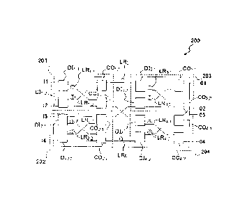
Figure 2 describes a feeding circuit 200 with four inputs 11,12,13,14 and
four outputs 01,02,03,04.
The circuit 200 of Figure 2 comprises four assemblies
201,202,203,204 of two dividers, two combiners and two delay lines arranged
in the same manner as for the circuit 100 of Figure 1 with two inputs and two
outputs.
The four assemblies 201,202,203,204 are connected together in the
following manner. The output of a combiner C01,1 of the first assembly 201 is
connected to the input of a divider D13,1 of the third assembly 203 by way of
a
delay line LR5 of length equal to an eighth of the wavelength of the signal at
CA 02849852 2014-04-25
13
the microwave frequency. The output of a combiner CO2,2 of the second
assembly 202 is connected to the input of a divider D14,2 of the fourth
assembly 204 by way of a delay line LR6 of length equal to an eighth of the
wavelength of the signal at the microwave frequency. The output of a
.. combiner C01,2 of the first assembly 201 is connected directly to the input
of
a divider 014,1 of the fourth assembly. The output of a combiner CO2,1 of the
second assembly 202 is connected directly to the input of a divider 013,2 of
the third assembly.
The four assemblies 201,202,203,204 are arranged so that the
transfer function of the feeding circuit 200 according to the invention is
equal
Jffe j3n e _Et e_pn\
. 4. 2 4
1 e 7 1
to the orthogonal matrix T= ¨ .0 4 e 2 where p is
the
2p e- 2 e- 4 1 _p_i
e 4
\e -j3: e.4 e- 3: 1 /
amplitude loss factor introduced previously.
As a function of the activated input 11,12,13,14, that is to say of the input
on which a signal is injected, the signals obtained on the four outputs
01,02,03,04 have equal power and are regularly mutually phase shifted by
a constant phase shift which is a multiple of P1/4.
The circuit represented in Figure 2 can be generalized to any
distributed feeding circuit with N inputs and N outputs, N being a power of 2,
by increasing the number of assemblies 201,202,203,204 to a number equal
.. to (N/2)log2(N) and by mutually interconnecting them by means of delay
lines
of length equal to a multiple of the wavelength of the signal at a microwave
frequency divided per 2N.
Figure 3 represents a diagram of a variant embodiment of the feeding
.. circuit 200 of Figure 2.
In order to further improve the compactness of the circuit according to
the invention by decreasing the number of hardware components required,
CA 02849852 2014-04-25
14
the assembly formed by a combiner and a divider mounted in series is
replaced by a coupler with two inputs and two outputs.
For example, the assembly formed of the combiner C01,2 and divider
D14,1 connected in series is replaced with a single coupler CP1,2. Likewise
the
assembly formed of the combiner CO2,1 and divider D13,2 connected in series
is replaced with a single coupler CP2,1. The assembly formed of the combiner
C01,1 and divider DI3,1 connected in series by way of a delay line LR5 is
replaced with a single coupler CP1,1 whose two outputs are connected to two
delay lines LR5,1 and LR5,2 of the same length equal to an eighth of the
113 wavelength of the signal at the microwave frequency. The assembly formed
of the combiner CO2,2 and divider DI4,2 connected in series by way of a delay
line LR6 is replaced with a single coupler CP2,2 whose two outputs are
connected to two delay lines LR6,1 and LR6,2 of the same length equal to an
eighth of the wavelength of the signal at the microwave frequency.
The couplers CP1,1, CP1,2, CP2,1, CP2,2 used are optical couplers which
do not introduce any appreciable phase shift, on the scale of the microwave
frequency domain, between the two signals delivered by their two respective
outputs.
Two delay lines LR5,2, LR3,2 mounted in series can be replaced with a
single delay line of length equal to the sum of the lengths of the two lines.
Another advantage of this variant embodiment is that dispensing with
the combiners C01,1 C01.2 CO2,1 CO2,2 makes it possible to avoid losses in
power when the input signals of the combiners are not phase-coherent.
Figure 4 represents a diagram of a feeding circuit 400 with eight inputs
and eight outputs according to the invention.
The circuit 400 described in Figure 4 is derived from the circuit 300
described in Figure 3 by doubling the number of inputs and outputs.
The circuit 400 comprises eight optical dividers, each connected to an
input 11,..., 18 of the circuit 400 and eight optical combiners, each linked
to an
output 01,..., 08 of the circuit 400. The circuit 400 furthermore comprises
CA 02849852 2014-04-25
two stages of eight dual-input and dual-output optical couplers. The various
hardware components of the circuit 400 are connected together, either
directly, or by way of delay lines of length equal to a multiple of the
distance
d'=ARF/16 where ARE is the wavelength of the signal at the microwave
5 frequency. In Figure 4 are indicated the precise values of the lengths of
the
various delay lines as a multiple of the length d'.
The assembly of hardware components of the circuit 400 is arranged
so that the theoretical transfer function T of the circuit is the orthogonal
matrix
represented in Figure 4bis, where p is the amplitude loss factor.
An objective is that the signals obtained at the output of the circuit 400
must be regularly mutually phase shifted by a constant phase increment
equal to a multiple of PI/8. The value of the phase increment depends on the
input I1,..., 18 activated.
Figure 4 represents an exemplary distributed feeding circuit with eight
inputs and eight outputs according to the invention. The dual-input and dual-
output couplers are used, as indicated for the example of Figure 3, to
decrease the number of hardware components required. Without departing
from the scope of the invention, they can be replaced, as explained for the
example of Figure 2, by an assembly composed of an optical combiner and
an optical divider connected in series.
The examples of Figures 1,2,3 and 4 are given by way of illustration,
for the proper understanding of the invention, but must not be interpreted as
limiting the subject of the invention to these examples alone. In particular,
the
invention can be extended to any distributed feeding circuit comprising a
number N of inputs and of outputs, N being a power of two, and whose
transfer function is an orthogonal or unit matrix when the loss factor is
equal
to 1. In a first variant embodiment, the feeding circuit according to the
invention is composed of a plurality of assemblies, such as described in
Figure 1, mutually interconnected directly or by way of delay lines of length
CA 02849852 2014-04-25
16
equal to a multiple of the distance d'=ARF/(2N) where ARF is the wavelength of
the signal at the microwave frequency. In a second variant embodiment, the
assembly composed of an optical combiner and of an optical divider
connected in series can be replaced with a dual-input and dual-output optical
coupler as illustrated in Figures 3 and 4.
Figure 5 represents another variant embodiment of the feeding circuit
of Figure 4.
The optical combiners forming the last stage of hardware components
ir) of the feeding circuit according to the invention may exhibit losses
due to the
fact that the signals that they receive at input are not phase-coherent.
Stated
otherwise, an optical combiner cannot perform a coherent recombination of
two signals if they are not phase-coherent.
A means of solving this problem is to replace each optical combiner
with a multiplexer of optical frequencies or more generally with a frequency-
selective means making it possible to combine two signals on two different
optical carriers. As an example, such a means can take the form of an optical
interleaver or "wavelength interleaver", of a Mach-Zehnder interferometer or
of any equivalent device able to multiplex several optical frequencies.
The signals produced on the various inputs 11,...18 of the circuit 500
according to the invention are modulated on different optical carriers.
Denoting by Al,... A8, the wavelengths associated with the optical carrier
frequencies of each of the eight input signals of the circuit 500, it is
possible
to perform various associations between the optical carrier frequencies and
the inputs of the circuit. By making the assumption that Al> A2> A3> A4> A5>
A6> A7> A8, a possible choice consists in assigning the optical carrier
frequencies to the inputs 11,...18 in increasing order of their value. The
following table illustrates the assignment of the optical carriers to the
various
inputs:
11 12 13 14 15 16 17 18
Al A2 A3 A4 A5 A6 A7 A8
CA 02849852 2014-04-25
17
By making this choice, the signals obtained on each output 0 1,...08 of the
circuit 500 will arise from the combination of a low optical frequency and of
a
high optical frequency.
Another possible choice consists in interleaving the optical carriers
before assigning them to the various inputs 11, ...18 of the circuit 500. The
following table illustrates the assignment of the optical carriers to the
various
inputs for this second choice:
11 12 13 14 115 16 17 18
Al A3 A5 A7 A2 A4 A6 A8
By making this second choice, the signals obtained on each output 01,...08
of the circuit 500 will arise from the combination of two adjacent optical
frequencies.
Other choices are possible regarding the order of assignment of the
optical wavelengths to the inputs of the circuit, but the two examples
mentioned hereinabove exhibit the advantage of facilitating the embodiment
of the multiplexers placed at the output of the feeding circuit.
Indeed it is observed on following the path of the signals in the
example of Figure 5 that for the first case of assignment of the optical
carriers
according to an increasing order of their values, each multiplexer receives on
its upper input a signal carried by an optical wavelength 21 to X4, and on its
lower input a signal carried by an optical wavelength 2.5 to X.8. The eight
multiplexers Ml,... M8 can therefore be identical multiplexers of two adjacent
sub-bands, also dubbed 'diplexers'.
For the second case of assignment of the optical carriers according to
a prior interleaving, the eight multiplexers M1,... M8 can be multiplexers
with
periodic transfer function, known by the term "wavelengths interleaver". Such
a device can be embodied in the guise of discrete hardware component or be
implanted on the same PIC optical circuit as the circuit according to the
invention.
CA 02849852 2014-04-25
18
Figure 5bis illustrates the operating principle of a wavelengths-
interleaving multiplexer 501. On the right of Figure 5bis is represented a
diagram of the spectrum at the output of the eight multiplexers M1,... M8.
This
spectrum comprises two sets of interleaved optical carriers 510,520. The first
set 510 corresponds to the odd wavelengths and the second set 520
corresponds to the even wavelengths.
The exemplary embodiments of the invention described hereinabove
in support of Figures 1 to 5 are all based on a feeding circuit according to
the
invention with two inputs and two outputs, one output of which is phase-
shifted with respect to the other output by +/- 90 and whose transfer
function
is given by the matrix T= ( 1 and an
exemplary implementation is
Thif ¨ j 1
given in Figure 1. By convention, such a circuit is named a 90 coupler.
Without departing from the scope of the invention, the 90 coupler of
Figure 1 can be replaced with any other device carrying out the function of a
coupler and whose transfer function is orthogonal or unitary (when the
combiners used are loss-free).
For example, another possible basic device is a 180 hybrid coupler
pi.2 11 11
whose transfer function is given by the matrix T'= _( )and which
provides as output two equi-amplitude signals which are either in phase, or in
phase opposition (that is to say phase-shifted by 180 ) instead of a phase
shift of +/- 90 as for the device of Figure 1.
Such a device can be embodied in the same manner as that
presented in Figure 1 except for the difference that the two delay lines
LR1,LR2 have a different length. The first delay line LR1 has a length equal
to half the wavelength of the signal at the microwave frequency. The second
delay line LR2 has a zero length, stated otherwise this second delay line can
be dispensed with.
CA 02849852 2014-04-25
19
On the basis of this variant of the basic device according to the
invention with two inputs and two outputs, it is possible to construct, as
indicated in Figures 2 to 5, distributed feeding circuits according to the
invention having an even number greater than two of inputs and of outputs.
The only modifications to be afforded to the circuits described in
Figures 2 to 5 are the lengths of the delay lines which are configured so that
the transfer function of the distributed feeding circuit obtained is given by
the
matrices presented in Figure 5ter.
The matrix T'a is the theoretical transfer function of a feeding circuit
according to the invention with 4 inputs and 4 outputs composed of 4 basic
hybrid couplers whose theoretical transfer functions are equal to T'.
The diagram of a distributed feeding circuit of theoretical transfer
function equal to T'4 is identical to the diagram of Figure 2 except for the
differences that the four assemblies 201,202,203,204 consist of 1800 hybrid
couplers according to the second variant of the invention, one of the two
additional delay lines LR5,LR6 is of length equal to a quarter of the
wavelength of the signal at the microwave frequency (stated otherwise to half
the length of a delay line of the basic 180 hybrid coupler) and the other
additional delay line LR5,LR6 is of zero length.
It is therefore seen that the design, according to the invention, of a
circuit with 4 inputs and 4 outputs on the basis of a 1800 hybrid coupler is
effected in a manner equivalent to that of the circuit of Figure 2 obtained on
the basis of a 900 coupler.
Likewise it is also possible to design a distributed feeding circuit with
eight inputs and eight outputs whose theoretical transfer function is the
matrix
T's and which is designed on the basis of several 180 hybrid couplers on the
same principle as that described in Figures 4 and 5.
By observing the matrix T'8, it is noted that, for each column, a phase
gradient makes it possible to pass from one line to the other:
-2Tr18, 6Tr/8, -6Tr18, 27/8, -41-r/8, 4-rr/8, -81-r/8,1
CA 02849852 2014-04-25
The values of the phase shifts obtained at the output of the 8x8 circuit are
therefore even multiples of Tr/8 and a sign alternation is present between two
adjacent outputs.
5 Figure 6 represents a diagram of an antenna beamforming array 600
comprising a distributed feeding circuit 601 according to the invention.
By way of illustration, the antenna beamforming array 600 described in
Figure 6 is adapted for feeding eight antennal elements 632,642 and
comprises a distributed feeding circuit 601 according to the invention with
10 eight inputs and eight outputs.
Each input 11,...18 is connected to an optical modulator 612,622, for
example a Mach-Zehnder modulator, which receives on an input an electrical
or microwave-frequency signal 610,620 previously optionally amplified by
way of an amplifier 611,621. The second input of each optical modulator
15 612,622 is connected to a generator of optical carriers 602 which is able
to
generate at least one optical carrier of wavelength Al. Advantageously, the
generator 602 is able to generate as many optical carriers as inputs of the
distributed feeding circuit 601. For example, the generator 602 may be able
to implement a wavelength multiplexing technique, or "wavelength division
20 multiplexing", so as to generate, in the example of Figure 6, eight
carriers at
eight wavelengths Al,... A8. Each optical carrier thus modulates the
microwave-frequency signal produced on one of the inputs of the circuit 601.
The signal obtained on each of the outputs 01,...08 of the circuit 601
is thereafter demodulated by way of an optical detector 630,640, for example
a photo-detector, able to convert the optical signal into an electrical signal
which is thereafter optionally amplified by way of amplifiers 631,641 before
being conveyed to the radiating elements 632,642 of the antennal array to be
fed.
Figure 7 illustrates the antenna radiation diagram obtained for an
antenna beamforming array of the type of that of Figure 6.
CA 02849852 2014-04-25
21
In Figure 7, two diagrams are represented, the first, in solid line,
corresponds to the use of a 900 basic coupler described in Figure 1, the
second, in dashed line, corresponds to the use of a 180 basic coupler as
explained in the description hereinabove.
Alongside each beam generated, the digit (ranging from 0 to 8)
indicates the multiplier coefficient of Tr/8 corresponding to the phase shift
between two adjacent outputs of the device. The letter (L or R) gives the
orientation (left or right) of the beam.
It is seen that the two basic coupler variants according to the invention
make it possible to design two complementary beamforming arrays.
Figure 8 shows schematically another variant embodiment of the
distributed feeding circuit according to the invention with four inputs and
four
outputs and previously described in support of Figure 3.
The common elements of the circuits described in Figures 3 and 8
bear the same references.
In this new variant, the optical couplers CP1,1, CP1,2, CP2,1, CP2,2 are
replaced with a first series of optical interleavers INT2,1,
INT2,2,
and the optical combiners CO3,1, CO3,2, C04,1, C04,2 are replaced with a
second series of optical interleavers 1NT3,1, INT3,2, INT4,1, INT4,2. The
optical
interleavers are hardware components with four ports, two input ports and
two output ports. Their manner of operation is illustrated by the diagrams 801
and 802.
For an assembly of eight regularly spaced optical wavelengths Ai,...
Its, an optical interleaver INT1,1 of the first series is configured to route
one
wavelength out of two towards the first output port and the other wavelength
towards the second output port. This principle is illustrated in the diagram
801, the wavelengths hi, h, A5, 17, represented dashed are routed towards
the output port opposite the input port on which the signal is injected. On
the
contrary -2, -4, -6, -8, the wavelengths AAA
represented solid are routed towards
CA 02849852 2014-04-25
22
the direct output port with respect to the input port on which the signal is
injected.
The optical interleavers of the second series operate on the same
principle as those of the first series except for the difference that the
interleaving period is double that of the first series. The manner of
operation
is illustrated by the diagram 802. The first four optical wavelengths Ai, A2,
A3,
A4, are conveyed to the opposite output port and the following four optical
wavelengths A5, As, A7, As are conveyed to the direct output port.
The use of optical interleavers in place of couplers or combiners
makes it possible to avoid the possible losses on recombining the signals at
output.
The overall manner of operation of the distributed feeding circuit 800
according to the invention is described in Figure 8. On each input 11,12,13,14
of the circuit 800, an electrical signal modulating two different optical
wavelengths is produced. The conveying of the optical wavelengths to the
outputs of the circuit 800 is illustrated in Figure 8. The first two outputs
01,02
can receive the wavelengths A2, A3, As, A7. The last two outputs 03,04 can
.. receive the wavelengths ¨1A, ¨4 A, ¨5 A, ¨ As.
The circuit, described in Figure 8, according to the invention can be
generalized, without departing from the scope of the invention, to any circuit
with N inputs and N outputs, with N a power of two.
Figure 9 represents a diagram of an antennal device 900 operating in
reception.
Such a device 900 comprises a distributed feeding circuit 901
according to the invention and operates according to a similar principle to
that described in Figure 6 except that the device of Figure 6 relates to an
antenna' system operating in transmission.
CA 02849852 2014-04-25
23
The distributed feeding circuit 901 is identical to the distributed feeding
circuit 601 used for the beamforming array described in Figure 6 except for
the difference that it undergoes a mirror symmetry with respect to the
arrangement of the circuit 601 of Figure 6. Stated otherwise, its inputs
11,...I8
and its outputs 01,...08 are inverted.
Indeed in the circuit 601 used for the transmitter device of Figure 6,
the linear phase laws are obtained on the outputs Oi by feeding the inputs Ij;
but the inverse is not true. For an antenna in reception, such as described in
Figure 9, the linear phase laws must be sited on the side of the radiating
elements, that is to say on the side of the inputs Ij. The circuit 901
obtained
by mirror symmetry on the basis of the circuit 601 of Figure 6 fulfils this
function, since all the couplers of which it is composed are reciprocal
devices. It is fed through the ports lj using linear phase laws (generated
starting from the axes of the 8 nominal beams of the antenna) and the energy
converges respectively towards one of the 8 outputs. The arrangement of the
circuit 901 corresponds to the use of the circuit 601 of Figure 6 in reverse,
in
which the signals would propagate from right to left.
Each input 11,...I8 is connected to an optical modulator 912,922, for
example a Mach-Zehnder modulator, which receives on an input an electrical
or microwave-frequency signal 610,620 received by way of an antennal
element 932,942 and previously optionally amplified by way of an amplifier
911,921. The second input of each optical modulator 912,922 is connected to
a generator of optical carriers 902 which is able to generate at least one
optical carrier of wavelength M.
The signal obtained on each of the outputs 01,...08 of the circuit 901
is thereafter demodulated by way of an optical detector 930,940 for example
a photo-detector, able to convert the optical signal into an electrical signal
which is thereafter optionally amplified by way of amplifiers 931,941.
CA 02849852 2014-04-25
24
Figure 10 shows schematically a variant of the beamforming array
according to the invention and described in Figure 6.
The device 600* represented in Figure 10 is identical to that
represented in Figure 6 except for the following differences.
Each optical modulator 612,622 is no longer fed by continuous optical
carriers, but by optical carriers which are themselves modulated by a
frequency, or angular frequency, 000L of a microwave local oscillator and
generated by the generator 602. The optical modulators 612,622 then play
the role of optoelectronic mixers by receiving, on a first input, an
electrical or
microwave-frequency signal 610,620 at an intermediate frequency, or
angular frequency, 0)FI and on a second input the optoelectronic signal
generated by the generator 602. The principle of implementation of a function
of optoelectronic mixing by an optical modulator is known per se, for example
described in the publication "G. K. Gopalakakrishnan et al., A LiNb03
microwave-optoelectronic mixer with linear performance, IEEE MTT-S Dig,
1993, pp.1055-1058".
The device 600* of Figure 10 furthermore comprises, for each output
pathway, a filter 633,643 of the bandpass filter type, making it possible to
extract the frequency component 0ORF:=0)F1+030L of the output signal of the
feeding circuit 601.
Figure 11 represents a diagram of a multi-port amplification device
comprising two distributed feeding circuits according to the invention.
It is known that a distributed feeding circuit, of the Butler matrix type,
can serve to feed, not an antennal array, but an assembly of power
amplifiers, so as to average the instantaneous power which passes through
them.
A multi-port amplification device 1000 such as this can be designed by
using a distributed feeding circuit 1001 according to the invention, as shown
schematically in Figure 11.
CA 02849852 2014-04-25
The multi-port amplification device 1000 comprises a first distributed
feeding circuit 1001 according to the invention comprising eight inputs and
eight outputs (it being understood that this number can be broadened to
other values, as already explained in the description).
5 Each input
11,...18 is connected to an optical modulator 1012,1022, for
example a Mach-Zehnder modulator, which receives on an input an electrical
or microwave-frequency signal 1010,1020 previously optionally amplified by
way of an amplifier 1011,1021. The second input of each optical modulator
1012,1022 is connected to a generator of optical carriers 1002 which is able
113 to generate at
least one optical carrier of wavelength Al. Advantageously, the
generator 1002 is able to generate as many optical carriers as inputs of the
distributed feeding circuit 1001. For example, the generator 1002 may be
able to implement a wavelength multiplexing technique, or "wavelength
division multiplexing", so as to generate, in the example of Figure 11, eight
15 carriers at eight wavelengths Al,... A8. Each optical carrier thus
modulates
the microwave-frequency signal produced on one of the inputs of the circuit
1001.
The signal obtained on each of the outputs 01,...08 of the circuit
1001 is thereafter demodulated by way of an optical detector 1030,1040, for
20 example a photo-detector, able to convert the optical signal into an
electrical
signal which is thereafter optionally amplified by way of amplifiers 1031,1041
before being conveyed to the inputs 1*1 ,...1*8 of a second distributed
feeding
circuit 1003 whose transfer function is the inverse M-1 of that, M, of the
first
circuit 1001.
25 The phase laws
generated at the output of the first circuit 1001 are not
necessarily 'equidistant linear', but only mutually orthogonal.
The theoretical total gain in power of the amplification device 1000,
measured between an input S1 ,S8 and a corresponding output S'1,S'8, is
equal to the gain afforded by the subassembly composed of an optical
detector 1030,1040 concatenated with an amplifier 1031,1041.
CA 02849852 2014-04-25
26
This gain is to be weighted by the possible losses arising in the first
and second circuits 1001,1003 as well as those originating from any
imperfection of production leading as a consequence to the fact that the
transfer functions M and M-1 of the first and second circuits 1001,1003 are
not perfectly inverse.
Other uses of a distributed feeding circuit according to the invention
are possible. In particular, several circuits can be arranged in cascade so as
to produce a beam-former adapted for feeding a two-dimensional antennal
array, for example a planar or conformal array.