Note : Les descriptions sont présentées dans la langue officielle dans laquelle elles ont été soumises.
CA 02856647 2014-05-22
WO 2013/053699 PCT/EP2012/069956
- 1 -
Suppression of Back Reflection in a Waveguide
Field of the Invention
The invention relates to waveguides. More particularly, but not exclusively,
the
invention relates to the suppression of back reflections of radiation in a
waveguide
used in a spectrometer.
Background of the Invention
Waveguides are used to guide electromagnetic radiation from one component of a
device to another or to guide radiation within a component. One example of
device
which utilises a waveguide is a spectrometer.
Spectrometers are used in many applications for measuring properties of light
across a range of wavelengths. For example, a spectrometer can be used for
compositional analysis, by obtaining absorption or emission spectra for an
object of
interest. The presence and location of peaks within the spectra can indicate
the
presence of particular elements or compounds. Spectrometers are commonly used
for analysis at optical wavelengths, but can also be used at other wavelengths
such
as microwave and radio wavelengths.
Spectrometers are typically relatively complex and expensive devices that
require the
alignment of a number of moving parts to be controlled with high precision.
For
example, a typical spectrometer may focus light onto a diffraction grating to
split an
incident beam into separate wavelengths, and the diffraction grating may be
rotated
to a specific angle to direct light of a particular wavelength towards a
detector. In
recent years chip-based spectrometers have been developed which can be highly
miniaturised, have no moving parts, and can be manufactured using well-
established
lithography techniques. An example of such a spectrometer-on-a-chip is shown
in
Figure 1.
The chip spectrometer 100 comprises a substrate 110, onto which are patterned
a
waveguide 120 and a plurality of disk resonators 130 coupled to the waveguide.
Light enters the waveguide at a first end 120a and is guided towards a second
end
CA 02856647 2014-05-22
WO 2013/053699 PCT/EP2012/069956
- 2 -120b. The resonators are arranged such that portions of the light in the
waveguide
are coupled into the disk resonators 130. Each resonator 130 is arranged to
support
a resonant mode at a particular wavelength such that only light of that
wavelength is
coupled into the resonator 130. On top of each disk resonator 130 is an
electrode
140 for detecting current that is proportional to the amount of light present
in that
resonator. The current detected in each resonator therefore indicates the
amount of
light at that wavelength that was present in the input beam of light. Each
electrode
140 is further connected to a signal bond pad 150 for connecting the
spectrometer
100 to an external device for measuring the current. A portion of the light is
not
coupled into any of the resonators and reaches the second end 120b of the
waveguide. Back-reflections from the end of the waveguide may give rise to
interference within the spectrometer chip which degrades the performance of
the
spectrometer. A low reflective coating 160 is therefore evaporated or
sputtered onto
the second end 120b of the waveguide to stop back-reflections from light
reaching
the end of the waveguide. However, the application of the low reflective
coating
requires an additional processing step in the manufacture of the spectrometer.
The invention aims to improve on the prior art.
Summary of the Invention
According to the invention, there is provided a structure for guiding
electromagnetic radiation, comprising: a substrate; a waveguide provided on
the
substrate and having a first end for receiving electromagnetic radiation and a
second
end; and an anti-reflection region provided at the second end of the waveguide
on
the substrate, the length and the width of the anti-reflection region being
optimised
to suppress back reflection of radiation that reaches the second end of the
waveguide.
The back reflection in the waveguide is reduced as a result of the radiation
becoming unguided as it enters the anti-reflection region where the diverging
radiation field is absorbed by the material forming the anti-reflection
region. By
optimising the length and the width of the anti-reflection region, an
effective
reflectivity of almost 0% can be achieved.
CA 02856647 2014-05-22
WO 2013/053699 PCT/EP2012/069956
- 3 -
The waveguide and the anti-reflection region may be formed from the same
material. The waveguide and the anti-reflection region may be integrally
formed as a
single component. They may be provided on the substrate in the same processing
step. The waveguide and the anti-reflection region may be provided as part of
the
same layer. If the waveguide comprises more than one layers, the waveguide and
the
anti-reflection region may provided as part of the same layers. The layers may
include a quantum well.
The anti-reflection region may have a width substantially wider than a width
of the
waveguide. The anti-reflection region may further have a width substantially
greater
than a wavelength of the radiation in a material from which the anti-
reflection
region is formed. When the anti-reflection region is formed from the same
material
as the waveguide, the wavelength is also the wavelength of the radiation in
the
waveguide. For example, the anti-reflection region may have a width of at
least 3
times the wavelength of the radiation in the material from which the waveguide
and
the anti-reflection region are formed. The structure may be a semiconductor
based
structure and the anti-reflection region may have a width of at least 3 times
the
wavelength of the radiation in the semiconductor waveguide. More specifically,
the
wavelength based on which the dimensions of the anti-reflection region is
determined is not the free-space wavelength but the wavelength in the material
from
which the waveguide and the anti-reflection region is formed.
The anti-reflection region may have a length substantially longer than a
wavelength
of said electromagnetic radiation in a material from which the anti-reflection
region
is formed. When the anti-reflection region is formed from the same material,
the
wavelength is also the wavelength of the radiation in the waveguide. The anti-
reflection section may have a length of typically at least 5 times the length
of the
wavelength of the electromagnetic radiation. Of course, the longer the anti-
reflection region, the greater the proportion of radiation that is not back-
reflected.
When the waveguide and the anti-reflection region are formed from a
CA 02856647 2014-05-22
WO 2013/053699 PCT/EP2012/069956
- 4 -
semiconductor material, the wavelength of the radiation in the waveguide would
be
the wavelength of the radiation in the semiconductor material.
According to the invention there is provided a photonic component comprising
the
structure as described above.
According to the invention, there is also provided a chip comprising the
structure as
described above.
According to the invention, there is also provided a spectrometer comprising
the
structure described above. The spectrometer may further comprise a plurality
of
resonators provided on the substrate and coupled to the waveguide.
The plurality of resonators may be disk resonators
Brief Description of the Drawings
Embodiments of the invention will now be described, by way of example, with
reference to Figures 2 to 6 of the accompanying drawings, in which:
Figure 1 is a perspective diagram of a prior art spectrometer;
Figure 2 is a perspective diagram of a spectrometer with a waveguide
arrangement
according to some embodiments of the invention;
Figure 3 is a plan view of the waveguide arrangement according to the
invention;
Figure 4 shows a cross-section of the waveguide arrangement of Figure 3;
Figure 5 illustrates a propagating continuous wave pattern in the waveguide
arrangement according to the invention;
Figure 6a is a graph showing how the radiation intensity at a particular
location in
the waveguide varies with time; and
Figure 6b indicates the location in the waveguide where the intensity of
radiation
is monitored for the graph of Figure 6a.
Detailed Description
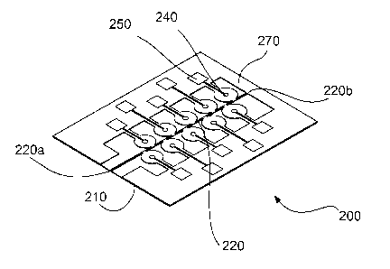
With reference to Figure 2, a perspective view of a spectrometer 200 with a
waveguide arrangement according to some embodiments of the invention is shown.
CA 02856647 2014-05-22
WO 2013/053699 PCT/EP2012/069956
- 5 -
The spectrometer is a spectrometer-on-a-chip comprising a substrate 210, onto
which are patterned an elongate waveguide 220 and a plurality of disk
resonators
230 coupled to the waveguide. The waveguide can be arranged to receive and
guide
electromagnetic radiation of a predetermined range of wavelengths, including
but
not limited to optical, microwave or radio wavelengths, and may be a ridge
waveguide. Light is received at a first end 220a of the waveguide and is
guided
towards a second end 220b, and each resonator 230 is arranged to support a
resonant mode at a particular wavelength such that only light of that
wavelength is
coupled into the resonator 230. On top of each disk resonator 230 is an
electrode
240 for detecting current that is proportional to the amount of light present
in that
resonator. The current detected in each resonator therefore indicates the
amount of
light at that wavelength that was present in the input beam of light. Each
electrode
240 is further connected to a signal bond pad 250 for connecting the
spectrometer
200 to an external device for measuring the current. It should be realised
that
although the resonators are described as separate from the waveguide, the
resonators may be considered part of the waveguide.
According to the invention, the spectrometer chip 200 also comprises an anti-
reflection region 270 coupled to the second end 220b of the waveguide 220. The
anti-reflection region provides an abrupt and wide interface at the end of the
waveguide so that waves propagating at the interface between the second end
220b
of the waveguide and the anti-reflection region 270 become unguided and
spreads
into the anti-reflection region where it diverges and becomes absorbed by the
anti-
reflection region. The anti-reflection region may be formed on the substrate
in the
same processing step as the waveguide and resonators. It may be provided in
the
same material or materials as the waveguide and the waveguide and the anti-
reflection region may be integrally formed as a single component. The
waveguide
and the anti-reflection region can be formed from, for example, semiconductor
material. The waveguide and the anti-reflection region can alternatively be
formed
from different materials. However, that would of course require an additional
processing step. Hereinafter, the waveguide and the anti-reflection region
will be
described as formed from the same material in the same processing step. The
anti-
reflection region 270 may be provided as an additional feature in the mask
layout of
CA 02856647 2014-05-22
WO 2013/053699 PCT/EP2012/069956
- 6 -
the spectrometer chip. The length and the width of the anti-reflection region
are
optimised to ensure that negligible back reflection of light occurs. Since the
back
reflection is effectively eliminated, or at least reduced using the anti-
reflection
region, a low reflective coating at the end of the waveguide is not required
and the
costly extra step of evaporating or sputtering the coating onto the waveguide
can be
avoided.
It will be appreciated that although the anti-reflection region 270 has been
described
with respect to a spectrometer 200 above, it can be used to provide a
mechanism
for reducing or eliminating back reflection in any photonic component. A
general
waveguide arrangement structure is shown with respect to Figure 3 and 4. With
reference to Figure 3, a light guiding section, provided by the waveguide 220,
is
directly connected to a radiation absorption section provided by the anti-
reflection
region 270. Both sections may be patterned on top of a substrate 210, as shown
in
Figure 4. The waveguide 220 and the anti-reflection region may be provided as
one
or a number of layers provided on top of the substrate as will be described in
more
detail below. The materials and the depths of the one or more layers are
selected to
guide the radiation in the waveguide without high losses but also such that
the
radiation is absorbed and scattered when the radiation becomes unguided and
diverges in the anti-reflection region.
As discussed above, the width and the length of the anti-reflection region 270
is
optimised to minimise back reflection of light reaching the end 220b of the
waveguide. It is contemplated that the anti-reflection region 270 may not
necessarily
form a rectangle but an irregular geometrical shape. The length is then
considered
the distance in the direction of propagation of the wave and the width is
considered
the distance in the direction perpendicular to the direction of propagation of
the
wave in the waveguide 220.
As shown in Figure 3, the width Wa of the anti-reflection region 270 is
selected to
be substantially wider than the width Wb of the waveguide 220. The waveguide
can,
for example, have a width of between 0.51.tm to 51.tm. The waveguide may be
designed to support a single mode of resonance. Typically, the width of the
CA 02856647 2014-05-22
WO 2013/053699 PCT/EP2012/069956
- 7 -
waveguide Wb is of the order of the wavelength of the radiation in a material
from
which the waveguide is formed. It may be substantially equal to, or slightly
larger
than, the width of the wavelength of the radiation in the material from which
the
waveguide is formed.
More importantly, the width Wa of the anti-reflection region 270 is
substantially
wider than the wavelength of the light or other radiation in the material from
which
the waveguide and the anti-reflection region are formed. The waveguide and
anti-
reflection region may be formed from a semiconductor material and the width Wa
may be significantly wider than the wavelength X, of the radiation in the
semiconductor material. The width of the anti-reflection region should be
sufficiently large to ensure that the radiation present in the anti-reflection
region is
no longer guided. The width Wa of the waveguide may be equal to or wider than
three times the wavelength X, of the radiation in the material from which the
waveguide and the anti-reflection region is formed to suppress back
reflections into
the waveguide. The input beam may include a plurality of wavelengths, for
example
when the device is a spectrometer as shown in Fig. 2. In such cases, the
wavelength
X, based on which the dimensions of the anti-reflection region are determined
may,
for example, be the mean wavelength, in the material of the anti-reflection
region,
of the wavelength range of interest in the input beam.
Moreover, the length of the anti-reflection region is longer than the
wavelength X, of
the radiation in the waveguide and the anti-reflection region. To eliminate
effectively all the back reflection, the length of the anti-reflection region
should be
at least five times larger than the wavelength X, of the radiation in the
semiconductor
from which the anti-reflection region is formed.
The waveguide and the anti-reflection region may be formed from a material
having
a refractive index substantially higher than air. If, for example, the
waveguide
comprises a semiconductor material having a refractive index of approximately
3
and the waveguide is arranged to receive radiation of wavelength 1500nm in
air, the
wavelength in the light guiding section would be approximately 500nm. It has
then
been found that a minimum length of the anti-reflection region, for
significantly
CA 02856647 2014-05-22
WO 2013/053699 PCT/EP2012/069956
- 8 -
reducing back reflection, would be 2.5 m. It is contemplated that a length of
approximately 31.tm would provide a suitable length for eliminating back
reflection
Moreover, the minimum width would be 1.5 1.tm. As mentioned before, it is
contemplated that as long as the distance of the anti-reflection region in the
direction of propagation of light is equal to or longer than 5 times the
wavelength X,
of the radiation in the material from which the anti-reflection region is
formed and
the width is equal to or wider than 3 times the wavelength X, of radiation in
the
material from which the anti-reflection region is formed, the amount of
reflected
radiation is significantly reduced.
Figure 4 shows a cross-section along the line Iv-Iv' of Figure 3. As shown, a
number of layers are deposited on top of the substrate 210. Figure 4 only
shows a
small number of layers and it will be appreciated that the structure can
include
additional layers. The waveguide may be deposited onto the substrate as one or
more layers. The waveguide 220 and the anti-reflection region 270 may extend
in
the same plane as the waveguide and be integrally formed with the waveguide.
The
substrate may be manufactured from any suitable type of semiconductor. For
example, the substrate may be formed from n-doped Indium Phosphide (InP) with
a
dopant concentration of about 1-3x 1018cm 3. On top of the substrate there may
be
provided an etch-stop layer (not shown), which prevents etching of the
substrate,
and on top of the etch-stop layer there may be provided a support layer (not
shown). As an example, an etch-stop layer may be formed from n-doped InGaAsP
with a dopant concentration of 0.18-1.2x 1018cm-3 and the support layer may be
formed from n-doped InP with a dopant concentration of 4-6x1017cm-3. The
waveguide 220 and the anti-reflection region 270 are then provided as one or
more
layers on top of the support layer. The layers may be formed from undoped
InGaAsP. On top of the one or more layers forming the waveguide there may be
formed a capping layer (not shown). The capping layer may be formed from p-
doped InP with a dopant concentration of about 2x1018cm-3. There may also be
provided an isolation layer for metallisation on top of the capping layer.
The one or more layers that provide the waveguide 220 and the anti-reflection
region 270 may have a higher refractive index than the support layer and the
CA 02856647 2014-05-22
WO 2013/053699 PCT/EP2012/069956
- 9 -
capping layer and the waveguide is formed from the refractive index contrast
between the layers forming the waveguide and the support layer and capping
layers.
It will be appreciated that the layer structure described above is just an
example and
one or more layers may be removed or replaced. For example, if the structure
does
not comprise a support layer, the waveguide and anti -reflection region is
provided
between the refractive index contrast between the waveguide layers and the
capping
layer and the substrate. The one or more layers forming the waveguide and the
anti-reflection region may comprise a layer with a band gap designed to absorb
the
radiation. It may be designed to have a low absorption coefficient to limit
the
absorption in the waveguide. When the light enters the anti-reflection region
it
becomes unguided. This means that the light travels over a greater distance
through
the absorbing layer and more of it is absorbed. Some of the light scatters,
some of it
back reflects from the semiconductor/air interface but then scatters further
and
undergoes more absorption on the way back. In other words, the key concept is
that
the light travels a greater distance through lossy material in the anti-
reflection
region and is strongly absorbed.
The one or more layers may form an active layer stack comprising two cladding
layers between which an active absorbing layer is sandwiched. The absorbing
layer
may be a quantum well with a band gap designed to absorb the radiation in the
anti-
reflection region. The quantum well may be grown by molecular beam epitaxy or
chemical vapour deposition which can control the layer thickness down to
monolayers. The quantum well would be sufficiently thin to have little or no
influence on the optical field in the waveguide. For example, the quantum well
may
have a thickness of approximately 3nm. The radiation that enters the anti-
reflection
region 270 is absorbed in the quantum well provided in the anti-reflection
region.
The waveguide 220 ensures that the optical field is at a maximum over the
quantum
well which helps to increase absorptions.
If the waveguide arrangement of Figures 3 and 4 is provided in the
spectrometer of
Figure 2, the resonators 230 would also include some or all of the layers
described
for the waveguide 220 and the anti-reflection region 270. The capping layer,
the
support layer and the cladding layers may have band gaps that are greater than
the
CA 02856647 2014-05-22
WO 2013/053699 PCT/EP2012/069956
- 10 -
highest-energy photon of interest. In contrast, as mentioned above, an active
layer
sandwiched between the cladding layers may have a band gap that is less than
the
lowest-energy photon of interest, i.e. lower than the energy of a photon of
the
longest wavelength that the spectrometer is configured to detect. In this way,
the
composition of the active absorbing layer can be used in all disk resonators
in the
spectrometer. As mentioned above, when the absorbing layer is a quantum well,
it
is sufficiently thin to have little or no influence on the optical field in
the
waveguide. When light of a particular wavelength enters the resonator from the
waveguide, it travels multiple cycles around the resonator and the photons can
be
absorbed by the material in the quantum well as the band gap is sufficiently
low for
even the lowest-energy photons to excite electrons from the valence band into
the
conduction band, generating electron-hole pairs. The resulting current can be
measured, and is proportion to the amount of light energy in the disk
resonator.
However, it will be appreciated that the structure does not have to be uniform
across the resonators 230, the waveguide 220 and the anti-reflection region
270. For
example, in some embodiments the absorbing layer is not provided in the
waveguide
220. To achieve this, the absorbing layer in the waveguide can be selectively
etched
and replaced by a wider band-gap alloy or the absorbing layer can only be
deposited
in the disk resonators and/or the anti-reflection region in the first place.
It should of course be realised that the present invention is not limited to
the layer
structure shown in Figure 3 and described above, and in other embodiments
other
structures may be used.
Figure 5 shows the results of a simulation illustrating the effect of a
2.51.tm long and
31.tm wide anti-reflection region on radiation with a wavelength of
approximately
500nm in the semiconductor material from which waveguide and anti-reflection
region are formed. The x-axis indicates the distance in a direction
perpendicular to
the direction of propagation of the wave in the waveguide and the y-axis
indicates
the distance in the direction of propagation of waves in the waveguide. It is
clear
from Figure 5 that the radiation diverges as it enters the anti-reflection
region. It is
further clear from Figure 5 that the light diverges over an area substantially
wider
CA 02856647 2014-05-22
WO 2013/053699 PCT/EP2012/069956
-11 -
than the width of the waveguide. The region at the end of the waveguide
provides
an end-stop for the radiation and the back-reflection into the waveguide is
minimised.
Figure 6a shows the results of another simulation of a waveguide arrangement
comprising an anti-reflection region as shown in Figure 6b. Light is detected
by a
detector in a location near the end of the waveguide coupled to an anti-
reflection
region substantially wider than the waveguide, as shown in Figure 6b. The
location
where the light is detected is indicated with an arrow. The graph of Figure 6a
shows
the intensity of detected light against time. It is clear from Figure 6a that
a pulse of
light is detected as the light received in the waveguide is guided through the
waveguide towards the anti-reflection region and that virtually 0% of the
light that
reaches the end of the waveguide is reflected back into the waveguide.
Whilst specific examples of the invention have been described, the scope of
the
invention is defined by the appended claims and not limited to the examples.
The
invention could therefore be implemented in other ways, as would be
appreciated by
those skilled in the art.
For example, it will be appreciated that the spectrometer, with respect to
which
embodiments of the invention have been described, may be considered to be, or
form part of, a spectrophotometer. Therefore, where the term "spectrometer"
has
been used, the term could have been replaced with the term
"spectrophotometer".
Moreover, although the spectrometer has been described in places to receive
and
guide light, the spectrometer can be used to guide and detect electromagnetic
radiation of any wavelength. Additionally, although the spectrometer has been
described to comprise disk resonators, the described waveguide may be used to
guide light into any type of resonators. For example, the resonators may be
any high
Q cavities, such as spherical resonators, microrings etc.
It should be realised that although the invention has been described with
respect to
a spectrometer on a chip, the invention can be implemented in any device that
uses
CA 02856647 2014-05-22
WO 2013/053699 PCT/EP2012/069956
- 12 -
a waveguide for guiding photons and in which back reflections are undesirable.
For
example, the invention could be used in an interferometer, optical switches,
lasers,
gratings etc. The invention could be used in any photonic component that
utilises a
waveguide. A photonic component is any component that generates, emits,
transmits, modulates, processes, switches, amplifies detects and senses light.
The
photonic component can, for example, be used in a photonic integrated circuit,
an
optical sensor or in an optical communication device, including but not
limited to
an Add-Drop Multiplexer for an optical communication device.