Sélection de la langue

Search

Sommaire du brevet 2857527 

Énoncé de désistement de responsabilité concernant l'information provenant de tiers

Une partie des informations de ce site Web a été fournie par des sources externes. Le gouvernement du Canada n'assume aucune responsabilité concernant la précision, l'actualité ou la fiabilité des informations fournies par les sources externes. Les utilisateurs qui désirent employer cette information devraient consulter directement la source des informations. Le contenu fourni par les sources externes n'est pas assujetti aux exigences sur les langues officielles, la protection des renseignements personnels et l'accessibilité.

Disponibilité de l'Abrégé et des Revendications

L'apparition de différences dans le texte et l'image des Revendications et de l'Abrégé dépend du moment auquel le document est publié. Les textes des Revendications et de l'Abrégé sont affichés :

  • lorsque la demande peut être examinée par le public;
  • lorsque le brevet est émis (délivrance).
(12) Demande de brevet: (11) CA 2857527
(54) Titre français: DISPOSITIF POUR PROTECTION CONTRE LES DEFAILLANCES DANS DES DISPOSITIFS D'ECLAIRAGE AYANT DES DIODES ELECTROLUMINESCENTES
(54) Titre anglais: DEVICE FOR FAILURE PROTECTION IN LIGHTING DEVICES HAVING LIGHT EMITTING DIODES
Statut: Réputée abandonnée et au-delà du délai pour le rétablissement - en attente de la réponse à l’avis de communication rejetée
Données bibliographiques
(51) Classification internationale des brevets (CIB):
  • H05B 47/25 (2020.01)
  • H05B 45/37 (2020.01)
(72) Inventeurs :
  • YAO, GANG (Etats-Unis d'Amérique)
  • TAO, HONGSHAN (Etats-Unis d'Amérique)
(73) Titulaires :
  • GENERAL ELECTRIC COMPANY
(71) Demandeurs :
  • GENERAL ELECTRIC COMPANY (Etats-Unis d'Amérique)
(74) Agent: CRAIG WILSON AND COMPANY
(74) Co-agent:
(45) Délivré:
(86) Date de dépôt PCT: 2011-11-10
(87) Mise à la disponibilité du public: 2013-05-16
Requête d'examen: 2016-09-09
Licence disponible: S.O.
Cédé au domaine public: S.O.
(25) Langue des documents déposés: Anglais

Traité de coopération en matière de brevets (PCT): Oui
(86) Numéro de la demande PCT: PCT/CN2011/082056
(87) Numéro de publication internationale PCT: CN2011082056
(85) Entrée nationale: 2014-05-30

(30) Données de priorité de la demande: S.O.

Abrégés

Abrégé français

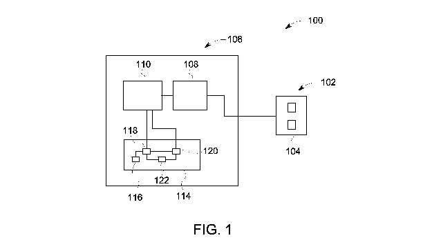
L'invention porte sur un dispositif d'éclairage, lequel dispositif comprend un moteur de lumière (102) avec une ou plusieurs diodes électroluminescentes (104), un circuit d'attaque (108) couplé au moteur de lumière (102) et alimentant le moteur de lumière (102) avec un courant de signal d'attaque, et un dispositif de protection (114) couplé au circuit d'attaque (108). Le dispositif de protection (104) comprend un commutateur de défaut (234) ayant une position qui maintient le courant de signal d'attaque à un niveau qui permet la poursuite du fonctionnement du moteur de lumière (102) pendant une condition de défaillance dans le dispositif d'éclairage ou en dessous de ce niveau.


Abrégé anglais

A lighting device comprises a light engine (102) with one or more LEDs (104), a drive circuit (108) coupled to the light engine (102) and energized the light engine (102) with a drive signal current, and a protection device (114) coupled to the drive circuit (108). The protection device (104) comprises a fault switch (234) having a position that maintains the drive signal current at or below a level that permits continued operation of the light engine (102) during a failure condition in the lighting device.

Revendications

Note : Les revendications sont présentées dans la langue officielle dans laquelle elles ont été soumises.


CLAIMS
What is claimed is:
1. A lighting device, comprising:
a light engine;
a drive circuit coupled to the light engine, the drive circuit energizing the
light
engine with a drive signal current; and
a protection device coupled to the drive circuit, the protection device
comprising a fault switch having a position that maintains the drive signal
current at
or below a level that permits continued operation of the light engine during a
failure
condition in said lighting device.
2. The lighting device of claim 1, wherein the failure condition is a short
circuit.
3. The lighting device of claim 1, wherein the failure condition occurs due to
a single component breakdown.
4. The lighting device of claim 1, wherein the input signal current meets
industry requirements set forth in Underwriters Laboratories class 2
specifications
during the failure condition
5. The lighting device of claim 1, further comprising a reset component to
actuate the fault switch at a pre-determined interval to cause the drive
signal current to
increase during the failure condition.
6. The lighting device of claim 5, wherein the reset component comprises a
reset switch coupled to the fault switch, and wherein the drive signal current
increases
when the fault switch is open and the reset switch is closed.
7. The lighting device of claim 5, further comprising a capacitor that
discharges to change the fault switch from closed to open.
8

8. The lighting device of claim 1, further comprising an opto-coupler coupled
to the drive circuit, wherein actuation of the opto-coupler causes the fault
switch to
open.
9. The lighting device of claim 1, wherein the protection device comprises a
comparator component coupled to the fault switch and a reference component
that
generates a reference voltage, and wherein the comparator component generates
a
switching signal with a switching voltage that closes the fault switch when
voltage
associated with the drive signal current falls below the reference voltage.
10. The lighting device of claim 1, wherein the fault switch comprises a metal
oxide field effect transistor.
11. A protection device for a lighting device, said protection device
comprising:
a comparator with a first input, a second input, and an output;
a fault switch coupled to the output; and
a reset switch coupled to the fault switch,
wherein the comparator generates a switching signal in response to a
difference in voltage between the first input and the second input that
actuates the
fault switch and the reset switch to maintain a drive signal current at or
below a level
that permits continued operation of the lighting device during a failure
condition.
12. The protection device of claim 11, wherein the comparator comprises an
op-amp.
13. The protection device of claim 11, further comprising a reference
component that provides a reference voltage to one of the first input and the
second
input, wherein the reference voltage provides a threshold that indicates a
fault
condition in the lighting device, and wherein the switching signal closes the
fault
switch in response to the fault condition.
9

14. The protection device of claim 11, further comprising a capacitor that
discharges voltage to close the reset switch at a pre-determined interval.
15. The protection device of claim 11, wherein the fault switch and the reset
switch comprise a metal oxide field effect transistor.
16. The protection device of claim 11, wherein the protection device is
coupled to a power supply.
17. A drive circuit for a lighting device, said drive circuit comprising:
a feedback circuit generating a feedback voltage in response to a drive
voltage
in the lighting device; and
a protection device coupled to the feedback circuit to receive the feedback
voltage, the protection device comprising a fault switch that opens in
response to a
decrease in the feedback voltage to maintain operation of the lighting device
during a
failure condition.
18. The drive circuit of claim 17, further comprising a converter coupled to
the feedback circuit, wherein the protection device generates an output signal
that
increases the operating frequency of the converter.
19. The drive circuit of claim 18, wherein the converter comprises a half-
bridge DC-DC converter.
20. The drive circuit of claim 17, wherein the protection device comprises a
reset component that closes the fault switch at a pre-determined interval.

Description

Note : Les descriptions sont présentées dans la langue officielle dans laquelle elles ont été soumises.


CA 02857527 2014-05-30
WO 2013/067704
PCT/CN2011/082056
DEVICE FOR FAILURE PROTECTION IN LIGHTING DEVICES HAVING
LIGHT EMITTING DIODES
BACKGROUND
Technical Field
[0001] The subject matter of the present disclosure relates to lighting
devices and,
more particularly, to failure protection (e.g., short circuit and component
breakdown)
for lighting devices with light emitting diodes (LEDs).
Description of Related Art
[0002] Light-emitting diodes (LEDs) are a popular light source. Examples of
LEDs include an LED chip which emits light, a color conversion module
including
translucent sealing materials (e.g. epoxy resin and/or silicone resin), and a
phosphor
layer that covers the LED chip. The emergence of LEDs that emit white light
make
LEDs more widely available for use in commercial and residential lighting
products.
LEDs and the lighting devices in which they are found have advantages such as
longer life, excellent responsiveness, and a compact configuration in
comparison with
incandescent lamps. Because LEDs are themselves a small and light-weight
configuration, the formation of thin and three-dimensional lighting fixtures
provides
further advantages such as enhancing a degree of freedom in the design of
lighting
fixtures.
BRIEF DESCRIPTION OF THE INVENTION
[0003] The present disclosure describes embodiments of a protection device
for
use with lighting devices that include light-emitting diodes (LEDs). These
protection
devices activate in response to a variety of failure conditions including
short circuit
conditions and component breakdown conditions. Moreover, protection devices of
the present disclosure meet industry requirements and standards, including,
but not
limited to: Underwriters Laboratories (UL) Class 2.
1

CA 02857527 2014-05-30
WO 2013/067704
PCT/CN2011/082056
[0004] Other features and advantages of the disclosure will become apparent
by
reference to the following description taken in connection with the
accompanying
drawings.
BRIEF DESCRIPTION OF THE DRAWINGS
[0005] Reference is now made briefly to the accompanying drawings, in
which:
[0006] FIG. 1 depicts a block diagram of an exemplary lighting device that
includes light-emitting diodes;
[0007] FIG. 2 depicts a schematic diagram of a topology for an exemplary
protection device for use in the lighting device of FIG. 1;
[0008] FIG. 3 depicts a schematic diagram of a topology for an exemplary
lighting device that includes the protection device of FIG. 2; and
[0009] FIG. 4 depicts a plot of voltage for various signals of a lighting
device
such as the lighting devices of FIGS. 1, 2, and 3.
[0010] Where applicable like reference characters designate identical or
corresponding components and units throughout the several views, which are not
to
scale unless otherwise indicated.
DETAILED DESCRIPTION OF THE INVENTION
[0011] FIG. 1 illustrates a block diagram of an exemplary lighting device
100
with features that prevent damage during failure conditions that can include
either or
both of short circuit conditions and single component breakdown conditions.
Such
failure conditions cause rapid changes in current and/or voltage that can
damage
components in the lighting device 100. In many cases, industry standards
(e.g.,
Underwriters Laboratories (UL) standards) define acceptable levels for such
changes
to protect against incidence of fire or other hazards. As discussed more
below,
embodiments of the lighting device 100 are configured to satisfy such industry
standards and, in one embodiment, address both short circuit conditions and
component breakdown conditions using a robust and cost-effective circuit
design.
2

CA 02857527 2014-05-30
WO 2013/067704
PCT/CN2011/082056
[0012] In FIG. 1, the lighting device 100 includes a light engine 102 with
one or
more light-emitting diodes 104 as the primary light source. The light engine
102
couples with a drive device 106 that provides a drive signal to operate the
LEDs 104.
The drive device 106 has components such as an LED driving circuit 108 and a
feedback circuit 110, both of which comprise various configurations of
discrete
electrical elements (e.g., resistors, capacitors, transistors, etc.). Failure
conditions can
occur when one or more of these elements fail or when a short-circuit occurs,
e.g., at
the light engine 102. These failure conditions often manifest themselves as
changes
to one or more operating conditions (e.g., current and/or voltage) of the
lighting
device 100 and, in particularly, to a rapid increase in drive signal current
at the light
engine 102.
[0013] To prevent failure and damage from the failure condition, a
protection
device 114 couples with the feedback circuit 110. The protection device 114
limits
the drive signal current in response to the short circuit as well as in
response to failure
of one or more electrical elements. In one example, the protection device 114
maintains the drive signal current at or below a level that permits continued
operation
of the light-emitting diode during the failure. The protection device 114
includes a
reference component 116, a comparator component 118 (e.g., an op-amp), and a
switching component 120 (e.g., a field effect transistor (FET) or a metal
oxide field
effect transistor (MOSFET)). These components can comprise combinations of
discrete electrical elements (e.g., resistors, capacitors, transistors, etc.),
an example of
which is shown by the topologies of FIGS. 2 and 3 below.
[0014] During operation of the lighting device 100, an external current
input (e.g.,
an alternating current (AC) input) energizes the lighting device 100. The
drive device
106 converts the AC input to the drive signal current, which causes the LEDs
104 to
emit light. The feedback circuit 112 monitors the drive signal current and
generates
an input signal that the protection device 114 receives. Changes in the
properties of
the input signal determine whether the protection device 114 limits the drive
signal
current. In one example, the comparator component 118 compares the input
signal to
a reference signal from the reference component 116. The comparator 118
generates
a switching signal that operates the switch component 120 between its open and
3

CA 02857527 2014-05-30
WO 2013/067704
PCT/CN2011/082056
closed positions. Deviation of the input signal from the reference signal
causes the
comparator 118 to change the switching signal, thereby causing the protection
device
114 to limit the drive signal current.
[0015] In one example, the protection device 112 also includes a reset
component
122, which couples with the switch component 120 to open and close the switch
component 120 at periodic or pre-determined intervals. A timing circuit or
other
configuration of components measure the pre-determined interval. The timing
circuit
can activate concurrently with the protection device 112 in response to the
failure
condition. Expiration of the pre-determined interval opens the switch
component 120
to remove the current limiting features of the protection device 114 from the
drive
device 106. The presence of the failure condition will cause the protection
device 114
to re-engage until the end of the next pre-determined interval. On the other
hand, if
the failure condition is no longer present, then the protection device 114
remains dis-
engaged and the lighting device 100 will continue to operate normally until
the next
failure occurs and the protection device 114 engages to limit the drive signal
current.
[0016] FIGS. 2 and 3 depict topologies for an exemplary lighting device
200. The
topologies show various components (e.g., resistors, capacitors, switches,
diodes, etc.)
that are useful for the present design. This disclosure does, however,
contemplate
other configurations of such components that would form topologies other than
that
shown the figures.
[0017] FIG. 2 focuses on the configuration of electrical elements for use
in an
exemplary protection device 214. In FIG. 2, the protection device 214 includes
a
reference component 216, a comparator component 218, a switching component
220,
and a reset component 222. Moving from left to right in the diagram, the
reference
component 216 includes a voltage supply 224, a resistor 226, and a capacitor
228.
These electrical elements generate a reference voltage Vr, which acts as a
threshold to
determine the operation of the protection device 200 as contemplated herein.
The
comparator component 218 includes an op-amp 230 having a first input that
receives
the reference voltage Vr. A second input of the op-amp 230 receives a feedback
voltage Vb from the feedback circuit (not shown). The op-amp 230 also has an
output
4

CA 02857527 2014-05-30
WO 2013/067704
PCT/CN2011/082056
that couples with the switch component 220 and the reset component 222. During
operation, the op-amp 230 compares the reference voltage and the feedback
voltage to
deliver a switching signal from the output to the switch component 220 and the
reset
component 222.
[0018] In the example of FIG. 2, the switch component 220 includes a fault
switch 234 that is responsive to the switching signal. The reset component 222
includes resistors (e.g., resistor 236 and resistor 238), a capacitor 240, a
diode 242,
and a reset switch 244. Both the fault switch 234 and the reset switch 244 can
comprise a MOSFET and/or related switching element. In one embodiment, the
switching signal changes the position of the fault switch 234 to lower the
properties of
an output signal that the protection device 214 provides to the drive circuit
206.
[0019] The topology of FIG. 3 shows details of an LED driving circuit 208
and a
feedback circuit 210 found in the lighting device 200. The feedback circuit
210
includes an opto-coupler 246 and a voltage divider 248 comprising resistors
(e.g.,
resistor 250, resistor 252, and resistor 254) and a capacitor 256. A regulator
circuit
258 couples to the voltage divider 248 and to the protection device 214. The
regulator
circuit 258 provides the feedback voltage Vb. In one example, the regulator
circuit
258 includes a resistor 260, a capacitor 262, and a regulator switch 264. The
feedback
circuit 210 also includes a Zener diode 266, a rectifier 268, and a
transformer 272.
The regulator circuit 258 provides a clamping voltage Va that controls
operating
frequency of a converter 276 (e.g., a half-bridge DC-DC converter) to get a
drive
voltage Vo that is appropriate for light-emitting diodes of the lighting
device 200.
[0020] In one example, failure conditions in the lighting device 200 will
cause the
feedback voltage Vb to drop below the reference voltage Vr. This drop causes
the
switching voltage of the switching signal from the op-amp 230 to exceed the
gate
voltage of the fault switch 242. The fault switch 234 closes in response to
the
switching voltage. Closing the fault switch 234 drives the clamping voltage Va
lower,
which changes the operating frequency of the converter 276. In one example,
the
operating frequency increases and can reach about 300 kHz or more. At these
operating frequencies, the drive signal voltage Vo and drive signal current
are reduced

CA 02857527 2014-05-30
WO 2013/067704
PCT/CN2011/082056
to levels that maintain and protect the components of the lighting device 200
and that
meet industry standards (e.g., UL standards).
[0021] FIG. 4 depicts plots of voltage for various components to help
describe
operation of the reset component 222. In FIG. 4, the plots show voltage for
each of
the clamping voltage Va, the switching voltage Vd, and a capacitor voltage Vc
for the
capacitor 228. Starting on the left side of the plots in FIG. 4, initiation of
the fault
condition causes the capacitor 228 to begin to charge, as evident by the
increasing
capacitor voltage Vc. When the capacitor 228 is fully charged, e.g., to the
threshold
or gate voltage of the reset switch 244, the reset switch 244 closes and the
fault switch
242 opens, which causes the clamping voltage Va to increase. The feedback
voltage
Vb also increases because of Miller effect principles at the regulator switch
264.
Artisans skilled in the electrical arts will recognize the Miller effect. When
the
feedback voltage Vb reaches the reference voltage Vr, the switching voltage Vd
drops
and the capacitor voltage Vc discharges through the output of the op-amp 230.
When
the Miller effect finishes, and if the fault condition is present, the
feedback voltage Vb
becomes low and the switching voltage Vd becomes high. In this configuration,
the
reset is complete and the reset component 222 begins another cycle.
[0022] As used herein, an element or function recited in the singular and
proceeded with the word "a" or "an" should be understood as not excluding
plural
said elements or functions, unless such exclusion is explicitly recited.
Furthermore,
references to "one embodiment" of the claimed invention should not be
interpreted as
excluding the existence of additional embodiments that also incorporate the
recited
features.
[0023] This written description uses examples to disclose embodiments of
the
invention, including the best mode, and also to enable any person skilled in
the art to
practice the invention, including making and using any devices or systems and
performing any incorporated methods. The patentable scope of the invention is
defined by the claims, and may include other examples that occur to those
skilled in
the art. Such other examples are intended to be within the scope of the claims
if they
have structural elements that do not differ from the literal language of the
claims, or if
6

CA 02857527 2014-05-30
WO 2013/067704
PCT/CN2011/082056
they include equivalent structural elements with insubstantial differences
from the
literal language of the claims.
7

Dessin représentatif
Une figure unique qui représente un dessin illustrant l'invention.
États administratifs

2024-08-01 : Dans le cadre de la transition vers les Brevets de nouvelle génération (BNG), la base de données sur les brevets canadiens (BDBC) contient désormais un Historique d'événement plus détaillé, qui reproduit le Journal des événements de notre nouvelle solution interne.

Veuillez noter que les événements débutant par « Inactive : » se réfèrent à des événements qui ne sont plus utilisés dans notre nouvelle solution interne.

Pour une meilleure compréhension de l'état de la demande ou brevet qui figure sur cette page, la rubrique Mise en garde , et les descriptions de Brevet , Historique d'événement , Taxes périodiques et Historique des paiements devraient être consultées.

Historique d'événement

Description Date
Inactive : CIB expirée 2022-01-01
Représentant commun nommé 2020-11-07
Demande non rétablie avant l'échéance 2020-10-08
Inactive : Morte - Taxe finale impayée 2020-10-08
Réputée abandonnée - omission de répondre à un avis sur les taxes pour le maintien en état 2020-08-31
Inactive : COVID 19 - Délai prolongé 2020-08-19
Inactive : COVID 19 - Délai prolongé 2020-08-06
Inactive : COVID 19 - Délai prolongé 2020-07-16
Inactive : COVID 19 - Délai prolongé 2020-07-02
Inactive : COVID 19 - Délai prolongé 2020-06-10
Inactive : COVID 19 - Délai prolongé 2020-05-28
Inactive : COVID 19 - Délai prolongé 2020-05-14
Inactive : CIB attribuée 2020-05-04
Inactive : CIB en 1re position 2020-05-04
Inactive : CIB enlevée 2020-05-04
Inactive : CIB attribuée 2020-05-04
Inactive : COVID 19 - Délai prolongé 2020-04-28
Inactive : CIB expirée 2020-01-01
Inactive : CIB enlevée 2019-12-31
Lettre envoyée 2019-11-12
Représentant commun nommé 2019-10-30
Réputée abandonnée - les conditions pour l'octroi - jugée non conforme 2019-10-08
Lettre envoyée 2019-04-08
Un avis d'acceptation est envoyé 2019-04-08
Inactive : Approuvée aux fins d'acceptation (AFA) 2019-03-27
Inactive : QS réussi 2019-03-27
Modification reçue - modification volontaire 2018-11-08
Inactive : Dem. de l'examinateur par.30(2) Règles 2018-05-09
Inactive : Rapport - Aucun CQ 2018-05-03
Modification reçue - modification volontaire 2017-12-04
Inactive : Dem. de l'examinateur par.30(2) Règles 2017-06-05
Inactive : Dem. de l'examinateur art.29 Règles 2017-06-05
Inactive : Rapport - Aucun CQ 2017-05-31
Lettre envoyée 2016-09-19
Requête d'examen reçue 2016-09-09
Exigences pour une requête d'examen - jugée conforme 2016-09-09
Toutes les exigences pour l'examen - jugée conforme 2016-09-09
Modification reçue - modification volontaire 2016-09-09
Inactive : Page couverture publiée 2014-08-08
Inactive : CIB en 1re position 2014-07-24
Inactive : Notice - Entrée phase nat. - Pas de RE 2014-07-24
Inactive : CIB attribuée 2014-07-24
Demande reçue - PCT 2014-07-24
Exigences pour l'entrée dans la phase nationale - jugée conforme 2014-05-30
Demande publiée (accessible au public) 2013-05-16

Historique d'abandonnement

Date d'abandonnement Raison Date de rétablissement
2020-08-31
2019-10-08

Taxes périodiques

Le dernier paiement a été reçu le 2018-10-24

Avis : Si le paiement en totalité n'a pas été reçu au plus tard à la date indiquée, une taxe supplémentaire peut être imposée, soit une des taxes suivantes :

  • taxe de rétablissement ;
  • taxe pour paiement en souffrance ; ou
  • taxe additionnelle pour le renversement d'une péremption réputée.

Les taxes sur les brevets sont ajustées au 1er janvier de chaque année. Les montants ci-dessus sont les montants actuels s'ils sont reçus au plus tard le 31 décembre de l'année en cours.
Veuillez vous référer à la page web des taxes sur les brevets de l'OPIC pour voir tous les montants actuels des taxes.

Historique des taxes

Type de taxes Anniversaire Échéance Date payée
Taxe nationale de base - générale 2014-05-30
TM (demande, 2e anniv.) - générale 02 2013-11-12 2014-05-30
Rétablissement (phase nationale) 2014-05-30
TM (demande, 3e anniv.) - générale 03 2014-11-10 2014-10-22
TM (demande, 4e anniv.) - générale 04 2015-11-10 2015-10-20
Requête d'examen - générale 2016-09-09
TM (demande, 5e anniv.) - générale 05 2016-11-10 2016-10-19
TM (demande, 6e anniv.) - générale 06 2017-11-10 2017-10-17
TM (demande, 7e anniv.) - générale 07 2018-11-13 2018-10-24
Titulaires au dossier

Les titulaires actuels et antérieures au dossier sont affichés en ordre alphabétique.

Titulaires actuels au dossier
GENERAL ELECTRIC COMPANY
Titulaires antérieures au dossier
GANG YAO
HONGSHAN TAO
Les propriétaires antérieurs qui ne figurent pas dans la liste des « Propriétaires au dossier » apparaîtront dans d'autres documents au dossier.
Documents

Pour visionner les fichiers sélectionnés, entrer le code reCAPTCHA :


Pour visualiser une image, cliquer sur un lien dans la colonne description du document (Temporairement non-disponible). Pour télécharger l'image (les images), cliquer l'une ou plusieurs cases à cocher dans la première colonne et ensuite cliquer sur le bouton "Télécharger sélection en format PDF (archive Zip)" ou le bouton "Télécharger sélection (en un fichier PDF fusionné)".

Liste des documents de brevet publiés et non publiés sur la BDBC .

Si vous avez des difficultés à accéder au contenu, veuillez communiquer avec le Centre de services à la clientèle au 1-866-997-1936, ou envoyer un courriel au Centre de service à la clientèle de l'OPIC.

({010=Tous les documents, 020=Au moment du dépôt, 030=Au moment de la mise à la disponibilité du public, 040=À la délivrance, 050=Examen, 060=Correspondance reçue, 070=Divers, 080=Correspondance envoyée, 090=Paiement})


Description du
Document 
Date
(aaaa-mm-jj) 
Nombre de pages   Taille de l'image (Ko) 
Description 2014-05-29 7 295
Abrégé 2014-05-29 1 57
Dessin représentatif 2014-05-29 1 4
Dessins 2014-05-29 3 30
Revendications 2014-05-29 3 96
Revendications 2017-12-03 2 69
Revendications 2018-11-07 2 72
Avis d'entree dans la phase nationale 2014-07-23 1 193
Rappel - requête d'examen 2016-07-11 1 118
Accusé de réception de la requête d'examen 2016-09-18 1 177
Avis du commissaire - Demande jugée acceptable 2019-04-07 1 163
Avis du commissaire - non-paiement de la taxe de maintien en état pour une demande de brevet 2019-12-23 1 533
Courtoisie - Lettre d'abandon (AA) 2019-12-02 1 539
Courtoisie - Lettre d'abandon (taxe de maintien en état) 2020-09-20 1 552
Modification / réponse à un rapport 2018-11-07 5 150
PCT 2014-05-29 12 416
Modification / réponse à un rapport 2016-09-08 3 78
Demande de l'examinateur 2017-06-04 4 223
Modification / réponse à un rapport 2017-12-03 8 255
Demande de l'examinateur 2018-05-08 3 166