Note : Les descriptions sont présentées dans la langue officielle dans laquelle elles ont été soumises.
CA 02859973 2014-06-19
WO 2013/096424
PCT/US2012/070569
Sensored Cable for a Power Network
The invention relates to a cable for transmission of electrical power in power
networks, that is
equipped with a capacitive voltage sensor comprising a printed circuit board
element ("PCB
element") placed over an electrically isolated piece of conductive or
semiconductive material,
which is arranged on an insulating layer of the cable and which is operable to
form an electrode
of a sensing capacitor of the voltage sensor. It also relates to the use of a
printed circuit board
element for contacting a conductive or semiconductive layer of a power network
cable.
Operators of electrical power networks monitor the state of their networks
using sensors for
voltage and current on their installations and on individual cables. An early
example of a voltage
sensor for high-voltage and medium-voltage power cables is described in the
British patent
GB1058890, in which the insulated conductor of the cable and a field-sensing
probe electrode
are surrounded by a guard electrode, and in which the guard and probe
electrodes are
connected to the input terminals of a high-gain amplifier.
In the German patent application DE 3702735 Al, a voltage measurement device
for a cable
comprises capacitive voltage divider. One of the capacitors, a high-voltage
capacitor, is formed
by the insulation of the central conductor of the cable and the conductive
layer enveloping it. A
measuring capacitor is located between the conductive layer and the shielding
mesh of the
cable.
The Japanese published patent application JP 60256068 A2 is related to
measuring the
charged voltage of a high-voltage power cable. It discloses to peel off a part
of a shielding
electrode of a power cable to expose an insulator. A conductive or
semiconductive member is
partially wound around the outer peripheral surface of the insulator to form a
suspended
electrode. A lead wire is embedded in and connected to said electrode. (D8,
considered closest
prior art)
It is an objective of the present invention to improve the electrical and
mechanical contact
between a voltage sensor circuit and aconductive or semiconductive layer of a
cable, where the
conductive or semiconductive layer of the cable is operated as an electrode of
a sensing
capacitor of a capacitive voltage sensor.
i
CA 02859973 2014-06-19
WO 2013/096424
PCT/US2012/070569
The present invention provides a sensored cable for distribution of electrical
power in a power
network, the sensored cable comprising an inner conductor and an insulating
layer arranged
concentrically around at least an axial section of the inner conductor,
wherein the sensored
cable further comprises a capacitive voltage sensor for sensing a voltage of
the inner conductor,
characterized by the sensor including a printed circuit board element, the
printed circuit board
element being placed over an electrically isolated piece of conductive or
semiconductive
material, the electrically isolated piece of conductive or semiconductive
material being arranged
on the insulating layer of the cable and being operable to form an electrode
of a sensing
capacitor of the capacitive voltage sensor.
/0
A printed circuit board ("PCB") can establish electrical contact to the
electrically isolated piece of
conductive or semiconductive material in several locations. This avoids the
disadvantages of
having electrical contact only in one location on the piece of (semi-
)conductive material, namely
it avoids, firstly, problems resulting from a bad electrical contact in the
one location, if that one
contact is, e.g., incomplete, corroded, or damaged. In the case of, e.g.,
corrosion or damage, no
voltage or a lower voltage can be measured on the PCB, resulting in an
incorrect voltage
reading of the sensor. Secondly, it also avoids problems arising from the fact
that electrons
travelling from a rim of the (semi-)conductive piece to the one contact
location experience the
electrical resistance of the (semi-)conductive piece over a longer path. This,
in turn, may lead to
a voltage drop and eventually to a lower, i.e. less accurate, voltage being
measured on the
PCB.
In contrast, the sensored cable according to the invention, having a PCB, may
provide a large
number of contact points on various locations on the PCB, and thereby on
various locations on
the (semi-)conductive piece. This creates redundancy, so that a single
corroded, incomplete or
damaged contact point cannot lead to an erroneous measurement of the voltage.
Also, a large
number of contact points will shorten the path which electrons have to travel
from a rim of the
(semi-)conductive piece to the next closest contact location on the PCB. This
results in a much
smaller voltage drop and a higher accuracy of the voltage reading.
A sensored cable according to the invention, having a capacitive voltage
sensor comprising a
PCB, offers the further advantage that the PCB may be adapted to support a
plurality of
electronic components which may serve other purposes, e.g. components that
form electronic
circuits for temperature compensation.
2
CA 02859973 2014-06-19
WO 2013/096424
PCT/US2012/070569
A sensored cable is a cable in combination with a sensor or comprising a
sensor. A cable
according to the invention comprises an inner conductor for conducting
electrical power, and an
insulating layer, arranged concentrically around at least an axial section of
the inner conductor.
The insulating layer may be arranged directly on the inner conductor.
The sensored cable according to the invention comprises a capacitive voltage
sensor for
sensing a voltage of the inner conductor. The sensor may be suitable for
sensing a voltage of
the inner conductor in relation to electrical ground potential or in relation
to another electrical
potential.
/0
A capacitive voltage sensor comprises a sensing capacitor. In the sensored
cable according to
the invention, one electrode of the sensing capacitor may be the inner
conductor or an
electrically conductive element which is electrically connected to the inner
conductor of the
cable. The insulating layer of the cable may be operable to form a dielectric
of the sensing
capacitor. More broadly, a dielectric of the sensing capacitor may comprise a
portion of the
insulating layer of the cable.
The sensored cable according to the invention is characterized by the sensor
including a printed
circuit board element ("PCB element"). The PCB element is placed over an
electrically isolated
piece of conductive or semiconductive material (herein also referred to as
"(semi-) conductive
material"), which in turn is arranged on the insulating layer of the cable.
The PCB element may
be placed on the electrically isolated piece of (semi-) conductive material.
The piece of (semi-)
conductive material is operable to form an electrode of the sensing capacitor.
The PCB element
is thus in mechanical contact with the insulating layer via the piece of (semi-
) conductive
material. The piece of (semi-) conductive material may thus be arranged
between the PCB
element and the insulating layer. The piece of (semi-) conductive material
may, for example, be
a layer of (semi-) conductive material, i.e. it may have two opposed major
surfaces, e.g. first and
second major surfaces. The first major surface may be in mechanical contact
with the insulating
layer. The second major surface may be in mechanical contact with the PCB
element.
The piece of (semi-) conductive material may, for example, comprise an
electrically conductive
metal or an electrically conductive polymer. In particular, it may comprise a
layer of copper. The
electrically isolated piece of (semi-) conductive material may be affixed to
the insulating layer of
the cable by an adhesive. The adhesive may, for example, be a pressure-
sensitive adhesive or
a hotmelt adhesive.
3
CA 02859973 2014-06-19
WO 2013/096424
PCT/US2012/070569
The PCB element may be in electrical contact with the piece of (semi-)
conductive material. The
PCB element may comprise one or more contacts for electrically contacting the
piece of (semi-)
conductive material. The PCB element may comprise contacts for electrically
and mechanically
contacting the piece of (semi-) conductive material. The PCB element may
comprise a
capacitor. The capacitor may be electrically connected to the piece of (semi-)
conductive
material. The capacitor may be operable as a secondary capacitor in a
capacitive voltage
divider. The capacitive voltage divider may comprise the sensing capacitor and
the secondary
capacitor. The capacitor and/or the capacitive voltage divider may be
comprised in the
capacitive voltage sensor for sensing the voltage of the inner conductor.
The PCB element may be placed over or on the piece of (semi-) conductive
material such as to
establish electrical contact between the PCB element and the piece of (semi-)
conductive
material. The PCB element is placed over the piece of (semi-) conductive
material, i.e. it is
arranged directly adjacent to the piece of (semi-) conductive material and it
contacts the piece of
(semi-)conductive material mechanically. The PCB element may have two opposed
major sides.
This PCB element may be placed on or over the piece of (semi-) conductive
material such as to
establish electrical contact between the PCB element and the piece of (semi-)
conductive
material. The PCB element may be attached to the piece of (semi-) conductive
material. It may
alternatively be in a pressure contact with the piece of (semi-) conductive
material.
The PCB element may comprise a double-sided PCB, i.e. the PCB has opposed
first and
second major sides. Such a PCB element may be particularly advantageous in
that it saves
space, so that the PCB element can be integrated into the cable or kept in
close vicinity to the
cable, e.g. in a splice. A PCB element comprising a double-sided PCB may
electrically contact
the piece of (semi-) conductive material with the first side of the PCB. The
double-sided PCB
may comprise a contact on the first major side for electrically contacting the
piece of (semi-)
conductive material. The PCB may comprise a contact on the first major side
for electrically and
mechanically contacting the piece of (semi-) conductive material. The PCB may
comprise a
capacitor. The capacitor may be electrically connected to the piece of (semi-)
conductive
material. The capacitor may be operable as a secondary capacitor in a
capacitive voltage
divider. The capacitor may be arranged on the second major side of the PCB.
Such a capacitor,
which is arranged on the second major side may be electrically connected to a
contact for
electrically contacting the piece of (semi-) conductive material on the first
major side through, for
example, a via or an electrically conductive plated through-hole in the PCB.
4
CA 02859973 2014-06-19
WO 2013/096424
PCT/US2012/070569
The PCB element generally may comprise an exposed conductive region providing
an extended
two-dimensional surface contact area. The exposed conductive region may be in
mechanical
and electrical contact with the electrically isolated piece of (semi-)
conductive material in two
dimensions and over an extended area. The exposed conductive region providing
an extended
two-dimensional surface contact area is particularly advantageous for
establishing intimate
mechanical and electrical contact between the PCB element and the piece of
(semi-) conductive
material, because it provides many potential contact points and maximizes the
contact area,
which results in a more reliable contact, and less resistive losses. In
embodiments in which the
inner electrical resistance of the electrically isolated piece of conductive
or semiconductive
material is not negligible, this arrangement may provide for shorter paths
which electrons need
to travel through the piece of (semi-) conductive material before reaching a
contact point of the
PCB element. This may reduce the effect of the inner resistance of the piece
of (semi-)
conductive material and provide for a higher measurement precision. In
general, the fact that
the contact area of the PCB element is not a single conductive point, but a
conductive region
providing an extended two-dimensional surface contact area, enhances the
accuracy and
reliability of the voltage sensor. An extended two-dimensional surface contact
area may be
larger than the area of a single contact. It may, for example, have an area of
1 cm2 or more.
Because of its extension, it may touch the piece of (semi-) conductive
material in a great
number of contact points. These contact points may be distributed over the
extended two-
dimensional surface contact area. The exposed conductive region of the PCB
element forms a
contact for electrically and mechanically contacting the piece of (semi-)
conductive material.
The exposed conductive region of the PCB element may comprise a layer of
conductive metal,
e.g. gold, silver, or copper. In particular, it may comprise a copper layer.
The copper layer may
be gold-plated for enhanced electrical contact and/or for protection against
environmental
influences, e.g. against corrosion.
The exposed conductive region of the PCB element may provide a continuous
surface contact
area or a patterned, i.e. interrupted, non-continuous, surface contact area.
All parts of the
patterned surface contact area may be electrically connected with each other.
A patterned
surface contact area may require less conductive material for manufacturing
it, while having
only a negligible influence on reliability of the electrical contact and
resistive losses. A patterned
surface contact area may also enhance the mechanical flexibility of the PCB
element, thus
reducing the risk of layer cracking when the PCB is bent, and of flaking. In a
specific
embodiment, the exposed conductive region comprises a patterned gold-plated
copper layer.
5
CA 02859973 2014-06-19
WO 2013/096424
PCT/US2012/070569
The pattern of the surface contact area may, for example, be a grid with a
square-shaped or a
diamond-shaped pattern.
The PCB element may comprise a flexible portion. An exposed conductive region
as described
above may be arranged on the flexible portion. In particular, the PCB element
may comprise a
flexible PCB. A flexible portion of the PCB element and in particular a
flexible PCB may allow
the PCB element to conform better to the electrically isolated piece of (semi-
) conductive
material. This, in turn, enhances the electrical contact between the PCB
element and the piece
of (semi-) conductive material and thereby makes the contact more reliable,
reduces resistive
/0 losses, and facilitates higher accuracy of the voltage sensor. A
flexible portion of the PCB
element may also allow the PCB element to conform to cables of different
diameters. In a
specific embodiment, the PCB element comprises a flexible double-sided PCB.
In a specific embodiment of the invention, the sensored cable comprises a
conductive or
semiconductive layer (i.e., a "(semi-) conductive layer"), arranged
concentrically on at least a
portion of the insulating layer. The electrically isolated piece of (semi-)
conductive material
comprises a first portion of the (semi-) conductive layer of the cable. Thus,
not a separately
applied piece of (semi-) conductive is operable to form the electrode of the
sensing capacitor,
but a first portion of the (semi-) conductive layer of the cable is operable
to form the electrode.
This is a cost-effective solution. Also, the (semi-) conductive layer is
normally well attached to
the insulating layer and forms no voids between the insulating layer and the
(semi-) conductive
layer. This reduces electrical stress and reduces the risk of electrical
discharges, e.g. between
insulating layer and the (semi-) conductive layer, and subsequent damage to
the cable. The first
portion may extend along a full circumference of at least an axial portion of
the insulating layer.
The first portion of the (semi-) conductive layer may form a cylindrical
sleeve, arranged on a
portion of the insulating layer and coaxial with the inner conductor of the
cable.
The sensored cable according to the invention may further comprise additional
(semi-)
conductive material. That additional (semi-) conductive material may be
arranged concentrically
around at least an axial section of the insulating layer. It may be arranged
on either side of the
electrically isolated piece of (semi-) conductive material. The additional
(semi-) conductive
material may comprise two conductive or semiconductive axial sections. One or
both of these
sections may extend along a full circumference of at least an axial portion of
the insulating layer.
Some or all of the additional (semi-) conductive material may be affixed to
the insulating layer of
the cable by an adhesive. One or both of the two axial sections may be
electrically isolated from
6
CA 02859973 2014-06-19
WO 2013/096424
PCT/US2012/070569
the electrically isolated piece of conductive or semiconductive material by
non-conductive axial
sections.
For a cable, which comprises a (semi-) conductive layer, arranged
concentrically on at least a
portion of the insulating layer, the additional semiconductive material may
comprise at least
second portions of the (semi-) conductive layer. This is beneficial in that it
allows to use portions
of the (semi-) conductive layer of the cable as additional (semi-) conductive
material. Additional
materials thus does not need to be applied in a separate step. This may save
cost and time.
These second portions of the (semi-) conductive layer of the cable may extend
along a full
circumference of at least respective axial portions of the insulating layer.
One or both of the
second portions may by electrically isolated from the electrically isolated
piece of conductive or
semiconductive material by non-conductive axial sections. The additional (semi-
) conductive
material may be affixed to the insulating layer of the cable by an adhesive.
These second
portions of the (semi-) conductive layer of the cable may be affixed to the
insulating layer of the
cable by an adhesive, they may alternatively be coated or painted on the
insulating layer. They
may be co-extruded with the insulating layer.
For a cable, which comprises a (semi-) conductive layer, arranged
concentrically on at least a
portion of the insulating layer, the electrically isolated piece of (semi-)
conductive material and
the additional (semi-) conductive material may be formed out of the (semi-)
conductive layer of
the cable. This may be achieved, for example, by removing the cable jacket,
exposing the
(semi-) conductive layer, and removing two annular sections or axial portions
of the (semi-)
conductive layer such that the axial portion of the (semi-) conductive layer
between the removed
axial portions forms the electrically isolated piece of (semi-) conductive
material, and such that
the remaining axial portions of the (semi-) conductive layer adjacent to the
removed axial
portions form the additional semiconductive material.
The additional (semi-) conductive material may be electrically isolated from
the electrically
isolated piece of (semi-) conductive material by non-conductive axial
sections. These non-
conductive axial sections may comprise non-conductive material or a void.
In a further aspect, the invention also provides the use of a printed circuit
board element ("PCB
element") for electrically contacting a conductive or semiconductive layer of
a high-voltage or
medium-voltage power network cable, wherein the printed circuit board element
comprises an
exposed conductive region providing an extended two-dimensional surface
contact area, and
wherein the exposed conductive region is in mechanical and electrical contact
with the
7
CA 02859973 2014-06-19
WO 2013/096424
PCT/US2012/070569
conductive or semiconductive layer of the cable in two dimensions and over an
extended area.
Use of a PCB element for that purpose is advantageous because PCBs are adapted
to support
a variety of electrical or electronic components. This may allow signal
processing in close
vicinity to the cable. The use of a PCB element may make the use of other
specialized elements
supporting electric or electronic components obsolete. Also, PCBs can be
manufactured at
relatively low cost.
The PCB element may be flexible. A flexible PCB element can be easily bent to
conform around
a layer of a cable. The PCB element may comprise a flexible PCB. PCBs can
easily be provided
/0 with an exposed conductive region providing an extended two-dimensional
surface contact
area, using standard techniques.
A sensor voltage, that is indicative of the voltage of the inner conductor of
the cable, may be
generated on the PCB element. A sensor wire may be attached to the PCB for
transmitting the
sensor voltage from the PCB element to electric measurement circuitry outside
the PCB
element. A ground wire may be attached to an electrically grounded layer of
the cable for
connecting electrical ground to the electrical measurement circuitry. The
electric measurement
circuitry may be operational to determine the voltage of the inner conductor
versus ground. In
an embodiment, in which the cable comprises additional (semi-) conductive
material arranged
concentrically around at least an axial section of the insulating layer on
either side of the
electrically isolated piece of (semi-) conductive material, the ground wire
may be attached to the
additional (semi-) conductive material. In a specific embodiment, in which the
cable comprises a
(semi-) conductive layer, and wherein additional (semi-) conductive material
comprises a portion
of the (semi-) conductive layer, the ground wire may be attached to the (semi-
) conductive layer.
The invention will now be described in more detail with reference to the
following Figures
exemplifying particular embodiments of the invention:
Fig. 1 Perspective view of a sensored cable according to the invention,
showing a piece of
conductive material and a PCB contacting it;
Fig. 2 Cross-section of the sensored cable, the piece of conductive
material and the PCB of
Figure 1;
Fig. 3 Plan view of the underside of the flexible PCB of Figures 1 and
2;
Fig. 4 Plan view of the underside of an alternative flexible PCB;
Fig. 5 Perspective view of an alternative sensored cable according to
the invention; and
8
CA 02859973 2014-06-19
WO 2013/096424
PCT/US2012/070569
Fig. 6 Electrical circuit diagram of a voltage sensor according to the
invention.
Herein below various embodiments of the present invention are described and
shown in the
drawings wherein like elements are provided with the same reference numbers.
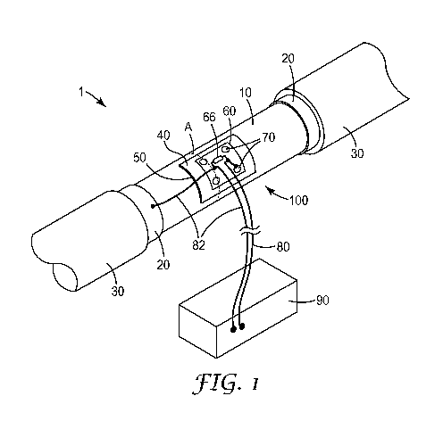
In the perspective view of Figure 1, a medium- or high-voltage power network
cable 1
comprises an electrically insulating layer 10, arranged around a central inner
conductor (not
visible in this Figure), a semiconductive layer 20 and an electrically
insulating cable jacket 30.
Along the length of the cable, these layers are arranged concentrically around
the inner
conductor. In the location of the cable shown in Figure 1, however, the cable
jacket 30 and the
semiconductive layer 20 have been removed along an axial section of the cable
1, so that the
insulating layer 10 is exposed. A piece of conductive material is arranged on
the exposed
insulating layer 10 of the cable 1, the piece forming a conductive patch 40.
The patch 40
conforms to the curvature of the insulating layer 10. In the axial direction
of the cable 1, it
extends such as to leave space between the patch 40 and the respective edges
of the
semiconductive layer 20. In the circumferential direction, it extends such as
to cover a fraction of
the insulating layer 10, about 25% of the circumference of the insulating
layer 10. The patch 40
of conductive material comprises a layer of copper, which forms a first
electrode of a sensing
capacitor of a voltage sensor 100, which can measure the voltage of the inner
conductor of the
cable 1, i.e. the voltage between the inner conductor and ground. The second
electrode of the
sensing capacitor is the inner conductor of the cable. The portion of the
insulating layer 10
located under the patch 40 forms the dielectric of the sensing capacitor. The
patch 40 is affixed
to the insulating layer 10 through a thin layer of adhesive 50 on the
underside (i.e. on the
radially inner side) of the patch 40 of conductive material.
A double-sided flexible PCB 60 is arranged on the radially outer side of the
patch 40 and
electrically and mechanically contacts the outer side of the patch 40. The PCB
60 conforms to
the curvature of the patch 40. The PCB 60 has, on its underside (i.e. its
radially inner side) an
exposed conductive region (not visible in Figure 1), through which it contacts
the outer side of
the patch 40. A plurality of so-called vies 70 provide conductive paths from
the exposed
conductive region on the underside to conductive traces on the upper side,
i.e. the radially outer
side, of the PCB 60. The upper side of the PCB 60 carries conductive traces
and electronic
components, in particular a secondary capacitor 66 which is connected in
series with the
conductive patch 40. The secondary capacitor 66 forms, in combination with the
sensing
capacitor described above, a capacitive voltage divider. The output voltage of
the capacitive
voltage divider serves to measure the voltage of the inner conductor of the
cable 1. This
9
CA 02859973 2014-06-19
WO 2013/096424
PCT/US2012/070569
measurement technique is in principle known. The electrical circuitry will be
described in greater
detail below. A sensor wire 80 transmits the output voltage of the capacitive
voltage divider from
the PCB 60 to a measurement device 90. A ground wire 82 provides an electrical
connection
from the semiconductive layer 20 via the PCB 60 to the measurement device 90.
The
semiconductive layer 20 is normally connected to electrical ground. By
determining the voltage
between the output of the capacitive voltage divider and ground, and by taking
into account the
electrical values of the sensing capacitor and of the secondary capacitor 66,
the measurement
device 90 can determine the voltage of the inner conductor versus ground in
known ways. The
inner conductor, the semiconductive layer 20, the sensing capacitor, the
secondary capacitor
/0 66, and the PCB 60 form a capacitive voltage sensor 100. The sensing
capacitor is formed by
the inner conductor and the isolated conductive patch 40 as electrodes, with
the insulating layer
being the dielectric of the sensing capacitor. The secondary capacitor 66 is a
regular
capacitor element, connected in series with the sensing capacitor and arranged
on the PCB 60.
The input of the secondary capacitor 66 is electrically connected to the
sensing capacitor and to
the sensor wire 80. The output of the secondary capacitor is electrically
connected to the ground
wire 82. The ground wire 82 is electrically connected to the semiconductive
layer 20 of the cable
1. The voltage measured between sensor wire 80 and ground wire 82 is
indicative of the voltage
between the inner conductor and ground.
The PCB 60 mechanically and electrically contacts the electrically isolated
conductive patch 40.
For good, i.e, low-ohmic electrical contact, it is desirable to have a
pressure contact between
the exposed conductive region 62 (shown in Figure 2) on the underside of the
PCB 60 and the
patch 40. The contact pressure should be high. In the embodiment shown, a
shrink sleeve (not
shown) is applied over the entire section of the cable in which the cable
jacket 30 is removed.
Before the shrink sleeve is applied and holds the PCB 60 in place, the PCB 60
can be
temporarily held in its position on the conductive patch 40 by a rubber band.
Once the shrink
sleeve is activated, i.e. shrunk down, it presses the PCB 60 onto the patch
40. The shrink
sleeve may comprise a conductive or semiconductive layer on its inside, which
contacts
electrically the exposed portions of the semiconductive layer 20 and connects
them electrically.
This layer of the shrink sleeve would then provide electrical stress control
in the area of the
cable 1 where the semiconductive layer 20 of the cable 1 is removed. However,
in this case the
PCB 60 must be electrically isolated from that (semi-) conductive inner layer
of the shrink
sleeve, e.g. by an isolating layer on top, i.e. on the outer side, of the PCB
60. This isolating layer
could be, e.g., an electrically insulating adhesive tape, that is wound around
the cable such as
to cover the PCB 60 and the conductive patch 40. For fixing the PCB 60 in an
alternative
manner, the PCB 60 may be shaped such that it extends along an almost full
circumference of
CA 02859973 2014-06-19
WO 2013/096424
PCT/US2012/070569
the insulating layer 10 plus the patch 40. This allows to fix one end of the
PCB 60 to the
opposed end of the PCB 60 with a piece of adhesive tape, so that the PCB 60 is
in tight
pressure contact with the patch 40.
Figure 2 is a cross-section of the sensored cable 1 of Figure 1, taken in the
plane indicated by
the letter "A" in Figure 1. For the sake of clarity, some radial dimensions
have been greatly
exaggerated. The inner conductor 5 of the cable 1 is surrounded concentrically
by the insulating
layer 10. The electrically isolated patch 40 is affixed adhesively, by
adhesive layer 50, to the
insulating layer 10. The flexible PCB 60 comprises the exposed conductive
region 62, on the
/0 underside of the PCB 60, and the PCB substrate 64. Two vias 70 are
visible, which provide
conductive paths from the exposed conductive region 62 through the substrate
64 to the upper,
radially outer side of the PCB 60, where conductive traces, the secondary
capacitor and other
electronic components are arranged.
Figure 3 shows, in plan view, the underside of the flexible double-sided PCB
60 of Figures 1
and 2. The exposed conductive region 62 is a continuous area which comprises a
gold-plated
copper layer and which covers a major part of the underside of the PCB 60. The
gold plating of
the exposed conductive region 62 is applied on a layer of copper. It serves to
provide high
electrical conductivity and protection against corrosion of the copper. The
gold plating is
arranged on the layer of copper and it faces away from the substrate 64 of the
PCB 60, while
the layer of copper is arranged between the substrate 64 and the gold plating.
At the margins of
the PCB 60, the non-conductive substrate 64 of the PCB 60 is exposed, i.e. it
is not covered by
the exposed conductive region 62. The vies 70 provide electrical connection
from the exposed
conductive region 62 through the substrate 64 to the opposite side of the PCB
60. Due to its
extension in two dimensions, the exposed conductive region 62 provides an
extended, two-
dimensional surface contact area of the PCB 60. Because of its extension, the
exposed
conductive region 62 can establish an extended, large surface contact with the
patch 40. The
large contact surface provides potentially a large number of points, where the
exposed
conductive region 62 and the patch 40 are in electrical contact. This makes
the electrical contact
reliable and potentially shortens the way which electrons have to travel
through the patch 40
before reaching a contact point and enter the exposed conductive region 62.
The exposed conductive region 62 on the underside of the PCB 60 may be
structured or
patterned, as opposed to the continuous exposed conductive region 62 shown in
Figure 3. An
example of a patterned exposed conductive region 62 is shown in plan view in
Figure 4. In this
embodiment, the patterned exposed conductive region 62 is formed by a
plurality of conductive
11
CA 02859973 2014-06-19
WO 2013/096424
PCT/US2012/070569
traces 110, arranged in a square-shaped pattern, i.e. a cross-hatch pattern,
which are
electrically connected to each other. The traces 110 thus form a conductive
mesh. Each
conductive trace 110 comprises a gold-plated copper layer, such that the gold
plating is
exposed and faces away from the substrate 64 of the PCB 60. The gold plating
is arranged on a
layer of copper, which is arranged on the substrate 64 of the PCB 60, so that
the layer of copper
is arranged between the substrate 64 and the gold plating. The conductive
traces 110 are
spaced about 1 mm from each other. This ensures that the exposed conductive
region 62
provides an extended, two-dimensional surface contact area of the PCB 60.
Because of its
extension, the exposed conductive region 62 can establish an extended, large
surface contact
/0 with the patch 40. The large contact surface, albeit patterned, provides
potentially a large
number of points, where the exposed conductive region 62 and the patch 40 are
in electrical
contact. This makes the electrical contact reliable and potentially shortens
the way which
electrons have to travel through the patch 40 before reaching a contact point
and enter the
exposed conductive region 62.
The space between the conductive traces 110 is left free, so that, in this
Figure, the substrate
64 of the PCB 60 is visible between the traces 110. The vias 70 provide
electrical connection
from the exposed conductive region 62 through the substrate 64 to the opposite
side of the PCB
60. The vias 70 are located such that each of them is in electrical contact
with at least one trace
110 of the exposed conductive region 62.
A patterned exposed conductive region 62 is believed to be more flexible than
a continuous
exposed conductive region 62. Bending of the PCB 60 may thus be easier, and
the PCB 60 may
thus conform better to the patch 40 on the insulating layer 10 of the cable 1.
Also, the patterned
exposed conductive region 62 shown in Figure 4 may be bendable around smaller-
radius bent
patches 40 without causing cracking or flaking of the PCB 60 or of one of the
layers which form
the exposed conductive region 62.
The PCB 60 differs from many common PCBs in that such PCBs have solder resist
layers
covering the front and back surfaces of the PCB, except for conductive areas
at which electrical
contacts (typically by soldering) can be made. In the PCB 60 of the embodiment
shown in
Figure 4, there is no solder resist on the underside of the PCB 60. A solder
resist layer on the
underside of the PCB 60, which typically inhibits flaking of the planar gold-
plating shown in
Figure 3, is not needed because the copper layer of the exposed conductive
region 62 is
patterned prior to gold plating. It is believed that the patterned copper
layer more easily
dissipates mechanical stress than does a solid copper foil.
12
CA 02859973 2014-06-19
WO 2013/096424
PCT/US2012/070569
Figure 5 is a perspective view of an alternative embodiment of a sensored
cable 1 according to
the invention. It is identical to the embodiment shown in Figures 1 and 2,
except for the
electrically isolated piece of conductive material and the presence of
additional semiconductive
material. While in Figure 1 the electrically isolated piece of conductive
material forms a patch
40, the electrically isolated piece of conductive material in Figure 5
comprises a portion of the
semiconductive layer 20 of the cable 1. That portion of the semiconductive
layer 20 extends
along a full circumference of an axial portion of the insulating layer 10. In
the embodiment
shown in Figure 5, the portion of the semiconductive layer 20 forms a
cylindrical sleeve 140,
/0 arranged on the insulating layer 10 and coaxial with the inner conductor
5 of the cable 1. In an
axial direction, the cylindrical sleeve 140 is separated from other portions
of the semiconductive
layer 20 by gaps 150 on either side of the sleeve 140. The gaps 150 are non-
conductive axial
sections. The sleeve 140 is thus electrically isolated from the other portions
of the
semiconductive layer 20 by the gaps 150. This arrangement makes the sleeve 140
operable to
form an electrode of a sensing capacitor of a voltage sensor 100, which can
measure the
voltage of the inner conductor 5 of the cable 1. The second electrode of the
sensing capacitor is
the inner conductor 5 of the cable. The portion of the insulating layer 10
located under the patch
40 forms the dielectric of the sensing capacitor. The sleeve 140 is affixed to
the insulating layer
10 in the same way as the other portions of the semiconductive layer 20 are
affixed to the
insulating layer 10. This may, for example, be coextrusion, coating or by an
adhesive. The
sleeve 140 has the same composition as the semiconductive layer 20. This is
because the
sleeve 140 is formed out of the originally continuous semiconductive layer 20
of the cable 1 by
removing two axial sections, i.e. the gaps 150, of that semiconductive layer
20.
In the embodiment shown, the gaps 150 in the semiconductive layer 20 are
formed by removing
axial sections of the originally continuous, uninterrupted semiconductive
layer 20 of the cable.
Thereby the gaps 150 provide electrical isolation of the sleeve 140 from the
other portions of the
semiconductive layer 20. This electrical isolation may also be achieved by
filling one or both of
the gaps 150 with a non-conductive material. The widths of the gaps 150, i.e.
their axial length,
may be chosen as appropriate. Normally, it is beneficial to have small gaps
150. This is
because the semiconductive layer 20 is a stress control layer. In the area of
the gaps 150, there
is reduced or no stress control by the semiconductive layer 20. This increases
the risk of locally
excessively high electrical field strength which may result in electrical
discharges and damage
to the cable 1. This risk is smaller if the gaps 150 are smaller.
13
CA 02859973 2014-06-19
WO 2013/096424
PCT/US2012/070569
The other portions of the semiconductive layer 20, on either side of the
sleeve 140, form
additional semiconductive material, arranged concentrically around the
insulating layer 10 on
either side of the sleeve 140. The gaps 150 separate this additional
semiconductive material
from the sleeve 140. The additional semiconductive material thus comprises two
portions of the
semiconductive layer 20 of the cable 1.
The PCB 60 is arranged on the outer surface of the sleeve 140. The PCB 60, its
fixation on the
sleeve 140, the sensor wire 80, ground wire 82 and the measurement device 90
are identical to
the corresponding elements and methods, as described in the context of Figure
1.
/0
Figure 6 is an electrical circuit diagram, showing the electrical
functionality of the various
elements of the capacitive voltage sensor 100, according to the present
invention. The sensing
capacitor 200 has a first electrode 201 and a second electrode 202. The first
electrode 201
corresponds to the inner conductor 5 of the cable 1, the second electrode 202
corresponds to
the electrically isolated piece of conductive or semiconductive material, e.g.
the patch 40 in
Figure 1 or the sleeve 140 in Figure 5. The sensing capacitor 200 is
electrically connected in
series with the secondary capacitor 66, which is arranged on the printed
circuit board element
60. The electrical contact between the printed circuit board element 60 and
the electrically
isolated piece of (semi-) conductive material is made via the exposed
conductive region 62 of
the printed circuit board element 60. Electrically, the secondary capacitor 66
is connected, on
one side, to the sensing capacitor 200 and, on the other side, to ground.
Voltage of the first
electrode 201 of the sensing capacitor 200 versus ground is measured by
measuring the
voltage across the secondary capacitor 66. The secondary capacitor 66 is
therefore electrically
connected to the measurement device 90 via the sensor wire 80 and the ground
wire 82. The
measurement device 90 is electrically connected in parallel to the secondary
capacitor 66 via
the sensor wire 80 and the ground wire 82. The measurement device 90 measures
the voltage
between the sensor wire 80 and the ground wire 82. The ground wire 82 is
electrically
connected to ground via a conductive or semiconductive element 220, which
corresponds to the
additional semiconductive material, e.g. a portion of the semiconductive layer
20 of the cable 1.
Element 220 is electrically connected to ground.
14