Note : Les descriptions sont présentées dans la langue officielle dans laquelle elles ont été soumises.
CA 02860077 2016-01-14
Asymmetric Field Ion Mobility Spectrometer
BACKGROUND OF THE INVENTION
1. Field of the Invention
The present invention relates to a technical field of ion migration, and
more particularly to an asymmetric field ion mobility spectrometer.
2. Description of the Related Art
Asymmetric field ion migration is a new type of ion migration technique. It
utilizes characteristic of mobility of charged molecular clusters varying with
intensity
of electrical field under the action of a strong electrical field, to identify
corresponding molecules. Typically, an asymmetric field ion mobility
spectrometer
is composed of two parallel electrodes and a collection electrode. The
parallel
electrodes each have a length less than 10mm, and a width less than 5mm, with
a
spacing of 0.5mm between them. The electrodes are formed by copper plated on
two pieces of glass plates. Ionized molecules enter into the electrodes under
the
action of uniform gas flow, and only the charged molecules satisfying a
specific
condition can reach the collection electrode through a gap between the
electrodes.
One piece of electrode is grounded while the other piece of electrode is
applied
with pluses having amplitude up to approximate 1000V and a pulse width of
dozens of nanoseconds, and at the same time is applied with a DC compensation
voltage. Only the ions which satisfy a condition of Kix ti =K2 x t2 can pass
the gap,
wherein K1 is an ion mobility under the strong electrical field, t1 is a high
voltage
pulse width, K2 is an inherent mobility under a weak electrical field, and t2
is a
weak electrical field pulse width. The aim of identifying substances can be
achieved
1
CA 02860077 2014-06-20
=
FP140114CA
by scanning the different ions released by the DC compensation voltage.
However, the above described asymmetric field ion mobility spectrometer
with parallel electrode plates cannot accurately distinguish peak positions of
different ions. Therefore, there is a need to have an ion mobility
spectrometer
having a new electrode structure.
SUMMARY OF THE INVENTION
Therefore, it is an object of the present invention to solve at least one
aspect of the above problems and defects in the prior art.
Accordingly, one object of the present invention is to provide an
asymmetric field ion mobility spectrometer, which can accurately identify peak
positions of different ions.
Another object of the present invention is to provide an asymmetric field
ion mobility spectrometer, which can identify different ions under the same
compensation voltage.
A further object of the present invention is to provide an asymmetric field
ion mobility spectrometer, which can reduce scanning time of the DC voltage.
In accordance with one aspect of the present invention, an asymmetric
field ion mobility spectrometer is provided, the asymmetric field ion mobility
spectrometer comprising:
an ionization source, for generating ions;
an electrode plate;
a plurality of electrode filaments, arranged in opposite to the electrode
plate and spaced apart from the electrode plate by an analysis gap, wherein a
high
voltage of electrical field is applied between the electrode plate and the
plurality of
electrode filaments to form an ion migration area, and the electrode filaments
are
2
CA 02860077 2014-06-20
FP140114CA
used to collect the ions that do not pass through the ion migration area; and
a collection electrode, disposed at a rear end of the ion migration area,
and collecting the ions that have passed through the ion migration area.
Specifically, the plurality of electrode filaments can comprise at least a
pair of reference filament and signal filament adjacent to each other, spaced
apart
from each other by a predetermined distance with a potential difference
between
them.
Further, the corresponding reference filament and signal filament in each
pair of the reference filament and signal filament can be respectively
connected to
two ends of an inductive coupler on the same side via capacitance, so that a
signal
about the ions collected by each signal filament is extracted out from the
other side
of the inductive coupler.
Specifically, the corresponding reference filament and signal filament in
each pair of the reference filament and signal filament can have a potential
difference equal to or less than 5V between them.
Specifically, a potential of the reference filament is OV, and a potential of
the signal filament may be +5V or -5V.
Further, the asymmetric field ion mobility spectrometer can comprise a
pair of introduction electrodes oppositely located at a front end of the ion
migration
area, and the ionization source is provided in a middle part of one
introduction
electrode in the pair of introduction electrodes.
Further, the analysis gap has a width of 0.5mm, the diameter of the
electrode filament is 0.1-0.3mm and the distance between the respective
adjacent
electrode filaments is 0.1-0.5mm.
3
CA 02860077 2014-06-20
=
FP140114CA
Further, the electrode plate can be a copper plating layer which is plated
on glass material or insulator, and the electrode filament is a copper
filament or a
copper filament plated on insulator.
Further, the ionization source is a radioactive source, a corona source or a
laser source.
Further, the ionization source is a corona pin.
Further, the asymmetric field ion mobility spectrometer can comprise a
controller, for applying an asymmetric high voltage RF waveform and DC
compensation voltage onto the electrode plate and the electrode filaments.
The above non-specific embodiments of the present invention at least
bring about one or more of the following advantages and effects: increasing
accuracy of identifying ion peak positions; reducing scanning time of DC
voltage
and types of the compensation voltage, thereby improving ion detection
efficiency.
BRIEF DESCRIPTION OF THE DRAWINGS
These aspects and/or other aspects as well as advantages of the present
invention will become obvious and readily understood from the description of
the
preferred embodiments of the present invention in conjunction with the
accompanying drawings below, in which:
Fig 1 is a structural schematic view of electrode structure in an
asymmetrical field ion mobility spectrometer in accordance with an embodiment
of
the present invention;
Fig. 2 is a schematic view of the electrode structure shown in Fig. 1 for
use with an ionization source;
4
CA 02860077 2014-06-20
FP140114CA
Fig. 3 is a view of simulation distribution result of three different ions A,
B
and C after passing through the electrode structure of Fig. 1;
Fig. 4 is a view of ion distribution result of three different ions A, B and C
captured on electrode filaments, wherein they are emitted at the same time;
and
Figs. 5a, 5b and 5c are respectively views of distribution results of ions A,
B and C having molecular weights of 127, 227 and 327, falling on the electrode
structure shown in Fig. 1.
DETAILED DESCRIPTION OF THE EMBODIMENTS
The technical solution of the present invention will be further explained in
detail, by the following embodiments, with reference to Figs. 1-5c. Throughout
the
specification, the same or similar reference numerals will indicate the same
or
similar components. The explanation to the implementations of the present
invention with reference to the accompanying drawing is intended to interpret
the
general inventive concept of the present invention, instead of limiting the
present
invention.
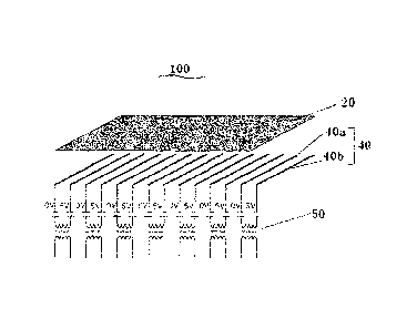
With reference to figures 1 and 2, the present invention provides an
asymmetric field ion mobility spectrometer 100 having a new electrode
structure. It
includes an ionization source 10 for generating ions; and an electrode plate
20. It
also includes a plurality of electrode filaments 40, which are positioned in
opposite
to the electrode plate 20 and spaced apart from it by an analysis gap d. A
high
voltage electrical field is applied between the electrode filaments and the
electrode
plate so as to form an ion migration area R. The electrode filaments 40 are
used to
collect ions which do not pass through the ion migration area R. It further
includes a
collection electrode 60, arranged at a rear end of the ion migration area R,
and for
collecting the ions which have passed through the ion migration area R.
In one embodiment, the plurality of electrode filaments 40 can include at
5
CA 02860077 2014-06-20
FP140114CA
least one pair of reference filament 40a and signal filament 40b positioned
adjacent
to each other. The corresponding reference filament 40a and signal filament
40b in
the pair are spaced apart with a predetermined distance (as shown) with each
other. There is a certain potential difference between the corresponding
reference
filament 40a and signal filament 40b in each pair. Preferably, the respective
reference filaments 40a and signal filaments 40b are arranged and spaced apart
in
one plane in an alternative manner. The skilled persons in the art will know
that the
electrode filament structure as described above can be manufactured by a
method
of tightening the filaments, etching the filaments and so on.
The corresponding reference filament 40a and signal filament 40b in each
pair of the reference filament and signal filament are respectively connected
to two
ends at a same side of an inductive coupler 50 via capacitance, so that a
signal
about ions collected by each signal filament 40b can be picked up/extracted
out at
the other side of the inductive coupler 50. Further, a potential difference
between
the corresponding reference filament 40a and signal filament 40b in each pair
can
be equal to or less than 5V.
In one embodiment, the potential difference between the corresponding
reference filament 40a and signal filament 40b in each pair can be equal to
5V.
Specifically, the potential of the reference filament 40a can be OV, and that
of the
signal filament can be +5V or -5V. The pair of the reference filament 40a and
signal
filament 40b as described above can be treated in a differential coupling so
as to
extract out the signal about the ions collected on the signal filament 40b
(served as
a collection filament). By such comparison and collection, charges are focused
on
each signal filament 40b, enhancing collection efficiency. As have been
described
above, up to thousands of RF electrical field will be applied on the electrode
plate,
causing very strong noise disturbance. As a result, only ions having
measurable
charge amount larger than the noise disturbance (i.e., meeting a certain
requirement on signal-to-noise), can be identified. Due to this, the
collection
6
CA 02860077 2014-06-20
=
FP140114CA
electrode in the prior art must be sufficiently large (for example, in a form
of bulk)
and the charge amount must be large enough to generate signal. However, such
arrangement has a poor resolution, and typically it is not possible to
perceive a
shape of a weak. The electrode filament structure directly eliminates the high
noise
disturbance generated by RF electrical field by such comparison method.
Therefore,
the present invention can generate signal, even if the signal filament and the
charge amount both are small, thereby improving resolving power. It can be
seen
from the result views of figures 3-5c that distribution of peak shapes can be
measured and the resolving power is improved.
It should be understood that the potential difference between the
reference filament 40a and the signal filament 40b is not limited to the value
as
described above; and it can be selected by the skilled person in the art as
required.
Specifically, with reference to figure 2, the asymmetric field ion mobility
spectrometer 100 in accordance with the present invention further includes a
pair of
introduction electrodes 70a and 70b oppositely arranged at a front end of the
ion
migration area R. More particularly, the pair of introduction electrodes
include an
upper introduction electrode 70a and a lower introduction electrode 70b. The
ionization source 10 is inserted into an immediate part of the upper
introduction
electrode 70a. In one embodiment, the ionization source 10 is inserted into a
circular hole of the upper introduction electrode 70a from an upper side
thereof.
In an embodiment of the present invention, the analysis gap can have a
width of 0.5mm, and the electrode filament can have a diameter in a range of
0.1-
0.3mm, and the spacing between respective adjacent electrode filaments can be
0.1-0.5mm. In one embodiment, the electrode plate has a length of 15mm, a
width
of 2mm, and a height of 0.5mm. Further, the electrode filament can have a
diameter of 0.1mm, and the spacing between the respective adjacent electrode
filaments is 0.1mm. The migration area has a length of 1.3mm-11.2mm. The
7
CA 02860077 2014-06-20
FP140114CA
spacing between the upper introduction electrode 70a and the electrode plate
20 is
0.1mm.
The electrode plate 20 can be a copper plating layer which is plated on
glass material or insulator, and the electrode filament 40 can be a copper
filament
or a copper filament plated on the insulator. The ionization source 10 can be
a
radioactive source, a corona source or a laser source. In one embodiment, the
ionization source 10 is a corona pin. It should be noted that when the
ionization
source 10 employs a pulsed corona source or laser, it requires to generate
ionized
clusters having a small pulse width; and when the ionization source 10 is a
radioactive source, it requires to achieve the pulsed ion clusters under a
control of
another electrode, while the generated ion cluster is very narrow along a
longwise
direction of the electrode plate.
In one embodiment, the asymmetric field ion mobility spectrometer in
accordance with the present invention further may include a controller (not
shown),
to apply asymmetric high voltage RF waveforms and DC compensation voltage
onto the electrode plate 20 and the plurality of electrode filaments 40.
With reference to figures 3-5c, the operating principle of the asymmetric
field ion mobility spectrometer of the present invention will be described
next:
It can be known from the above that when the potential of the reference
filament 40a is OV, if the potential of the signal filament 40b is positive,
the present
ion mobility spectrometer can identify and recognize negative ions (negative
ion
working mode); and if the potential of the signal filament 40b is negative,
the
present ion mobility spectrometer can identify and recognize positive ions
(positive
ion working mode).
Upon performing an ion identifying test, the ion source is disposed below
8
CA 02860077 2014-06-20
FP140114CA
the ionization source 10 as shown in figure 3, and the generated ion cluster
is
distributed along a longitudinal direction while the centre of the ion cluster
is
located in the middle of the upper and lower introduction electrodes 70a and
70b,
exhibiting Gauss Distribution with 0.4mm of FWHM(full width at half maximum).
In
the embodiment shown in figure 3, the ion cluster includes three kinds of
negatively
charged ions having molecular weights of 127, 227, and 327, respectively. The
number of each kind of negatively charged ions is approximately 500.
Under the action of the electrical field, when the ion cluster passes
io through the gap between the upper introduction electrode 70a and the
electrode
plate 20, it is focused, and then enters the ion migration area having the
analysis
gap or width d of 0.5mm. The lightest ions fall onto the signal filaments 40b
at the
front end of the ion migration area (i.e., the left side of figure 2, for
example an
entrance). The heavier ions fall onto the middle part of the ion migration
area and
the heaviest ions arrive at the collection electrode through the ion migration
area.
As shown in Figure 3, the ion A is the negative ion having a molecular
weight of 127; the ion B is the negative ion having a molecular weight of 227
and
the ion C is the negative ion having a molecular weight of 327. When the above
three kinds of ions are emitted at the same time, they would fall onto
different
signal filaments 40b, forming a certain distribution. Different peak positions
can be
clearly identified from figure 4, thereby distinguishing three kinds of
different ions
having different molecular weights from each other.
As shown in figures 5a-c, they respectively illustrate the peak positions of
the three kinds of ions on the signal filament 40b. Specifically, as shown in
figure
5a, the peak position of the ions having the molecular weight of 127 (a
displacement along the electrode filament in a longwise direction) is 2.2 mm,
FWHM (full width at half maximum) thereof is lmm, and the ions fall on the
signal
filaments at the front end of the ion migration area. As shown in figure 5b,
the peak
9
CA 02860077 2016-01-14
position of the ions having the molecular weight of 227 is 5 mm, FWHM thereof
is
4.5mm, and the ions fall on the signal filaments at the middle part of the ion
migration area. As shown in figure 5c, the ions having the molecular weight of
327
pass through the ion migration area and are collected by the collection
electrode at
the rear end of the ion migration area.
Please be noted that figures 4 and 5 are the views of the distribution result
of the ions A, B, and C falling onto the signal filaments of figure 1 under
the same
condition. The difference of figure 4 from figure 5 lies in the count of ions
A, B, and
C by the signal filaments (i.e., the ordinates of figures 4 and 5 are
different from
each other), while other conditions are identical. In other words, it can be
seen from
figures 4 and 5 that although their counts on the ions A, B and C are
different, both
of them can clearly identify the peak positions of the ions A, B and C.
Finally, they
can obtain the same identification result (i.e., the same peak positions for
ions A, B
and C).
It should be understood that the views of figures 4 and 5 are illustrative,
and they are mainly intended to explain the fact that the asymmetric field ion
mobility spectrometer as shown in figure 1 is capable of well identifying the
peak
positions of ions A, B and C.
By this method, it is possible to identify different kinds of molecules under
one compensation voltage, effectively improving resolution of substances by
the
asymmetric field ion mobility spectrometer, and reducing the range of scanning
voltage and shortening time. The asymmetric field ion mobility spectrometer in
accordance with the present invention not only can collect the ions passing
through
the ion migration area, but also can collect and analyze the ion not passing
though
the ion migration area.
10
CA 02860077 2016-01-14
. _
Although preferred embodiments of the invention have been disclosed for
illustrative purposes, those skilled in the art will appreciate that many
additions,
modifications, and substitutions are possible and that the scope of the claims
should not be limited by the embodiments set forth herein, but should be given
the
broadest interpretation consistent with the description as a whole.
11