Note : Les descriptions sont présentées dans la langue officielle dans laquelle elles ont été soumises.
1
CA 02860620 2014-07-04
WO 2013/105798 PCT/KR2013/000208
Description
Title of Invention: SMALL ANTENA APPARATUS AND
METHOD FOR CONTROLING THE SAME
Technical Field
Hi The present invention relates to small antenna technology using
circuit resonance in a
mobile terminal supporting various additional functions.
Background Art
[2] Generally, a mobile terminal may include various kinds of wireless
communication
units in order to perform wireless communication functions. In addition, the
wireless
communication units may perform the wireless communication functions using an
antenna corresponding thereto. Currently, the mobile terminal may include a
commu-
nication unit such as a Long Term Evolution (LTE) communication unit, a
Wideband
Code Division Multiple Access (WCDMA), and any other similar and/or suitable
type
of communication unit, for wireless communication with a base station, a commu-
nication unit such as a WiFi communication unit, a Wireless Broadband (Wibro)
com-
munication unit, a Worldwide Interoperability for Microwave Access (Wimax) com-
munication unit, and any other similar and/or suitable type of communication
unit, for
connection with the Internet network, a communication unit such as a Bluetooth
com-
munication unit, a Near-Field Communication (NFC) unit, and any other similar
and/or
suitable type of communication unit, for near field communications and/or
short range
communications, a GPS receiving unit, and any other similar and/or suitable
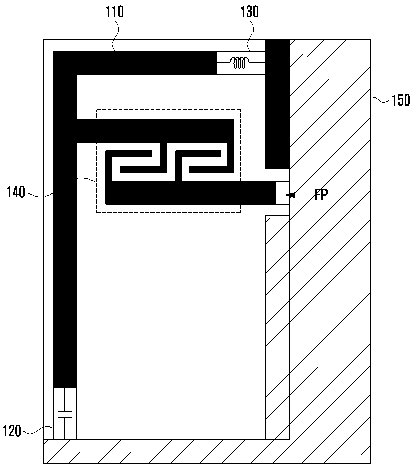
commu-
nication unit. The communication units as described above may include antennas
for
performing the wireless communication using Radio Frequency (RF) communication
with objects external to the mobile terminal. That is, the current mobile
terminal may
include a plurality of antennas for performing the wireless communication
functions.
Therefore, the antenna should be miniaturized and/or have a small size thereof
in order
to mount the plurality of antennas to the mobile terminal.
1131 A Planar Inverted F Antenna (PIFA) is a type of a small antenna. In
the case of the
PIFA type used in the mobile terminal, 1/4 wavelength of usable frequency is
needed.
For example, in the case of a GPS antenna, which has a frequency band of
1.575GHz,
a physical length of 4.7cm in the air is needed, and in the case of an LTE
antenna,
which has a frequency band of 700 MHz band, a physical length of 10.7cm in the
air is
needed. Therefore, since the mobile terminal of the related art should support
various
wireless communication functions including the plurality of antennas, there is
a
problem that the plurality of antennas may occupy a significant space of the
mobile
terminal. Accordingly, there is a limitation in manufacturing mobile terminals
having a
2
CA 02860620 2014-07-04
WO 2013/105798 PCT/KR2013/000208
plurality of antennas and a small size. In addition, since resonance of the
antenna may
be determined by the physical length of the antenna, a longer amount of time
may be
needed for tuning at the time of manufacturing design and development steps,
such as
a modification of a mold and the like.
[4] Therefore, a need exists for a system and method for small antenna
technology using
circuit resonance instead of wave resonance.
1151 The above information is presented as background information only to
assist with an
understanding of the present disclosure. No determination has been made, and
no
assertion is made, as to whether any of the above might be applicable as prior
art with
regard to the present invention.
Disclosure of Invention
Technical Problem
[6] Therefore, since the mobile terminal of the related art should support
various wireless
communication functions including the plurality of antennas, there is a
problem that
the plurality of antennas may occupy a significant space of the mobile
terminal. Ac-
cordingly, there is a limitation in manufacturing mobile terminals having a
plurality of
antennas and a small size. In addition, since resonance of the antenna may be
de-
termined by the physical length of the antenna, a longer amount of time may be
needed
for tuning at the time of manufacturing design and development steps, such as
a modi-
fication of a mold and the like.
Solution to Problem
1171 Aspects of the present invention are to address at least the above-
mentioned
problems and/or disadvantages and to provide at least the advantages described
below.
Accordingly, an aspect of the present invention is to provide a small antenna
apparatus
using circuit resonance instead of wave resonance by connecting an electric
circuit to
the antenna apparatus. Here, the small antenna may be a metal structure having
a pre-
determined pattern printed on a Printed Circuit Board (PCB) or formed on a
tool such
as a carrier.
1181 Another aspect of the present invention is to provide a small antenna
apparatus that
uses an electric circuit, such as a lumped element, an inter-digital circuit,
or the like,
positioned on the PCB at both ends of an asymmetrical antenna pattern
implemented
on the PCB or at both ends of an asymmetrical antenna pattern attached to the
tool and
a feeding line, thereby increasing both of an electrical wavelength and an
input
impedance matching.
1191 In accordance with an aspect of the present invention, an antenna
apparatus is
provided. The apparatus includes an antenna pattern, a first electric circuit
and a
second electric circuit respectively connected between both ends of the
antenna pattern
3
CA 02860620 2014-07-04
WO 2013/105798 PCT/KR2013/000208
and a system ground, and a third electric circuit disposed between the antenna
pattern
and a feeding line, wherein the first electric circuit, the second electric
circuit, and the
third electric circuit extend electrical wavelengths of the antenna pattern in
order to
increase input impedance matching.
[10] In accordance with another aspect of the present invention, a mobile
terminal is
provided. The mobile terminal includes an antenna apparatus including an
antenna
pattern, a first electric circuit and a second electric circuit respectively
connected
between both ends of the antenna pattern and a system ground, and a third
electric
circuit disposed between the antenna pattern and the feeding line, a
communication
unit for receiving a Radio Frequency (RF) parameter from a base station, a
memory for
storing a reference RF parameter therein; and a control unit for comparing the
received
RF parameter with the reference RF parameter and for changing a device value
of a
corresponding electric circuit, from among the first electric circuit, the
second electric
circuit and the third electric circuit of the antenna apparatus until a change
value
between the received RF parameter and the reference RF parameter satisfies a
reference RF parameter when the comparison value is out of the reference RF
parameter.
[11] In accordance with another aspect of the present invention, a mobile
terminal is
provided. The mobile terminal includes an antenna apparatus including a
antenna
pattern, a first electric circuit and a second electric circuit respectively
connected
between both ends of the antenna pattern and a system ground, and a third
electric
circuit disposed between the antenna pattern and a feeding line, a memory for
storing a
reference RF parameter therein, and a control unit for measuring an RF
parameter
which is outputted from the antenna apparatus, for comparing the measured RF
parameter with the reference RF parameter and for changing the device value of
the
electric circuit, from among the first electric circuit, the second electric
circuit and the
third electric circuit, of the antenna apparatus until a comparison value
between the
measured RF parameter and the reference RF parameter satisfies a reference
speci-
fication when the comparison value is out of the reference specification.
[12] In accordance with another aspect of the present invention, a method
for controlling
the resonance frequency of an antenna apparatus of a mobile terminal is
provided. The
method includes receiving an RF parameter from a base station, comparing the
received RF parameter with a reference RF parameter stored in a memory of the
mobile terminal, and changing the device value of a corresponding electric
circuit of an
antenna apparatus until a comparison value between the received RF parameter
and the
reference RF parameter satisfies a reference specification when the comparison
value
is not the reference specification. The antenna apparatus includes an antenna
pattern, a
first electric circuit and a second electric circuit respectively connected
between both
4
CA 02860620 2014-07-04
WO 2013/105798 PCT/KR2013/000208
ends of the antenna pattern and a system ground, and a third electric circuit
disposed
between the antenna pattern and a feeding line.
[13] In accordance with another aspect of the present invention, a method
for controlling a
resonance frequency of an antenna of a mobile terminal is provided. The method
includes measuring a output of an antenna apparatus including an antenna
pattern, a
first electric circuit and a second electric circuit respectively connected
between both
ends of the antenna pattern and a system ground, and a third electric circuit
disposed
between the antenna pattern and a feeding line, comparing the measured RF
parameter
with a reference RF parameter stored in a memory, and changing the device
value of a
corresponding electric circuit of the antenna apparatus until a comparison
value
between the measured RF parameter and the reference RF parameter satisfies a
reference specification when the comparison value is not the reference
specification.
[14] Other aspects, advantages, and salient features of the invention will
become apparent
to those skilled in the art from the following detailed description, which,
taken in con-
junction with the annexed drawings, discloses exemplary embodiments of the
invention.
Advantageous Effects of Invention
[15] The small antenna apparatus according to the exemplary embodiments
discussed
above has antenna pattern provided in the PCB or tool, connects the electric
circuit,
which may be at least one of or a combination of an active device and a
passive device,
on the PCB to the feeding line and to both ends of the antenna, such that the
size of the
antenna is reduced so as to efficiently utilize the space. Furthermore, a
circuit
resonance type operation may be used to perform the tuning of the electric
circuit
connected at the time of changing the resonance point, such that the antenna
resonance
frequency may be efficiently changed. Accordingly, the antenna apparatus
according to
the exemplary embodiments discussed above may reduce the antenna mounting
space
so as to provide a multi-function such that the antenna apparatus may be
efficiently
applied to the mobile terminal performing various wireless communication
functions.
In addition, at the time of changing the resonance point, not by using a
physical length
change of the antenna through the mold, but by tuning the connected electric
circuit,
the development time and cost of the mobile terminal may be reduced.
Brief Description of Drawings
[16] The above and other aspects, features, and advantages of certain
exemplary em-
bodiments the present invention will be more apparent from the following
detailed de-
scription taken in conjunction with the accompanying drawings, in which:
[17] FIG. 1 is a diagram illustrating a structure of a small antenna
according to an
exemplary embodiment of the present invention, and illustrating a structure of
a small
5
CA 02860620 2014-07-04
WO 2013/105798 PCT/KR2013/000208
antenna printed on a Printed Circuit Board (PCB);
[18] FIG. 2 is diagram illustrating a configuration of an equivalent
circuit of a small
antenna having a configuration such as the configuration shown in FIG. 1
according to
an exemplary embodiment of the present invention;
[19] FIG. 3 is a diagram illustrating a flow of current in an antenna at a
time of resonance
generation in a small antenna apparatus according to an exemplary embodiment
of the
present invention;
[20] FIG. 4 is a diagram illustrating a structure of a small antenna having
another structure
printed on a PCB according to an exemplary embodiment of the present
invention;
[21] FIG. 5 is a diagram illustrating a structure of a small antenna having
a configuration
of an antenna apparatus when an antenna is attached to a specific tool of a
mobile
terminal according to an exemplary embodiment of the present invention;
[22] FIG. 6 is a diagram illustrating a small antenna apparatus in which
input impedance
and a length of an antenna are matched to each other by connecting an electric
circuit
to both ends and a feeding ends of the antenna according to an exemplary
embodiment
of the present invention;
[23] FIGs. 7A and 7B are diagrams illustrating change characteristics of a
resonance point
due to a change of an electric circuit connected to both ends of an antenna in
an
antenna apparatus having a structure such as that shown in FIG. 6 according to
an
exemplary embodiment of the present invention;
[24] FIG. 8 is a diagram illustrating change characteristics of return loss
due to a change
of an electric circuit connected to a feeding point of an antenna apparatus
having a
structure such as that shown in FIG. 6 according to an exemplary embodiment of
the
present invention;
[25] FIG. 9 is a diagram illustrating a configuration of changing an
electric circuit in an
antenna apparatus according to an exemplary embodiment of the present
invention;
[26] FIG. 10 is a flowchart illustrating a procedure of changing an
electric circuit of an
antenna apparatus such as that shown in FIG. 9 according to an exemplary
embodiment
of the present invention;
[27] FIG. 11 is a diagram illustrating a configuration of a mobile terminal
having a small
antenna apparatus according to an exemplary embodiment of the present
invention;
and
[28] FIG. 12 is a flowchart illustrating a procedure of changing a
resonance frequency of
an antenna apparatus in a mobile terminal according to an exemplary embodiment
of
the present invention.
[29] Throughout the drawings, it should be noted that like reference
numbers are used to
depict the same or similar elements, features, and structures.
6
CA 02860620 2014-07-04
WO 2013/105798 PCT/KR2013/000208
Mode for the Invention
[30] The following description with reference to the accompanying drawings
is provided
to assist in a comprehensive understanding of exemplary embodiments of the
invention
as defined by the claims and their equivalents. It includes various specific
details to
assist in that understanding but these are to be regarded as merely exemplary.
Ac-
cordingly, those of ordinary skill in the art will recognize that various
changes and
modifications of the embodiments described herein can be made without
departing
from the scope and spirit of the invention. In addition, descriptions of well-
known
functions and constructions may be omitted for clarity and conciseness.
[31] The terms and words used in the following description and claims are
not limited to
the bibliographical meanings, but, are merely used by the inventor to enable a
clear and
consistent understanding of the invention. Accordingly, it should be apparent
to those
skilled in the art that the following description of exemplary embodiments of
the
present invention is provided for illustration purpose only and not for the
purpose of
limiting the invention as defined by the appended claims and their
equivalents.
[32] It is to be understood that the singular forms "a," "an," and "the"
include plural
referents unless the context clearly dictates otherwise. Thus, for example,
reference to
"a component surface" includes reference to one or more of such surfaces.
[33] The present invention relates to a small antenna apparatus that may be
used in a
mobile terminal supporting various wireless communication functions such as
Long
Term Evolution (LTE), Global Positioning Service (GPS), Bluetooth (BT), WiFi,
and
other similar and/or suitable wireless communication services. The small
antenna
apparatus, according to an exemplary embodiment of the present invention, has
a
structure connecting an electric circuit to both ends and/or a feeding point
of a prede-
termined pattern which may be printed and/or may be made of an iron structure
or any
suitable and/or similar material, formed on a tool such as a carrier or
printed on a
Printed Circuit Board (PCB), and may use a circuit resonance instead of a wave
resonance.
[34] The small antenna apparatus, according to an exemplary embodiment of
the present
invention, may use an electric circuit, such as a lumped element, an inter-
digital
circuitõ and any other similar and/or suitable electric circuit, positioned on
the PCB of
the mobile terminal for both ends of an antenna pattern and/or feeding line,
such that
an electrical wavelength and an input impedance are simultaneously improved,
thereby
making it possible to save approximately 50% of a space used by the small
antenna
apparatus of the exemplary embodiment of the present invention, as compared to
a
small antenna of the related art. In addition, tuning of a resonance point of
the antenna
may be performed through the electric circuit connected to the antenna
pattern, such
7
CA 02860620 2014-07-04
WO 2013/105798 PCT/KR2013/000208
that it may be unnecessary to spend time for generating a mold modification
time
during design and development of the small antenna apparatus according to an
exemplary embodiment of the present invention, thereby making it possible to
reduce a
development time. In the small antenna apparatus according to an exemplary em-
bodiment of the present invention, the feeding line may be connected to the
antenna
pattern through the inter-digital circuit instead of the lumped element that
may
generate unnecessary resonance, such that the input impedance may be increased
and a
tolerance of the existing lumped element may be reduced. The antenna pattern
of the
small antenna apparatus, according to an exemplary embodiment of the present
invention, may be an asymmetrical antenna pattern implemented on the PCB or
may be
the asymmetrical antenna pattern attached to a tool.
[35] As described above, the small antenna apparatus, according to an
exemplary em-
bodiment of the present invention, may have a structure in which an electric
circuit
may be connected to both ends of the antenna pattern and/or the feeding line
to which
signal is supplied. The antenna pattern may be an antenna pattern implemented
on the
PCB or an antenna pattern of the metal material attached to the tool. Further,
the
antenna pattern may be asymmetrically formed based on the feeding line in
order to
provide a degree of freedom in mounting. In addition, the electric circuit may
be a
circuit made of a combination of resistance R, inductor L, and capacitor C
that is a
passive device generating electrical resonance and may be a circuit made of a
com-
bination of at least one of a Field Effect Transistor (FET), a Bipolar
Junction
Transistor (BJT), and a diode that is an active device, and may be a circuit
made of a
combination of the passive device and the active device. The electric device
may have
a chip type or a package type and may be implemented as the inter-digital
structure im-
plemented on the PCB.
[36] FIG. 1 is a diagram illustrating a structure of a small antenna
according to an
exemplary embodiment of the present invention, illustrating a structure of a
small
antenna printed on a PCB.
[37] Referring to FIG., 1 the structure of the antenna apparatus may be
illustrated such
that a ground plane is not shown. Electric circuits 120 and 130 are connected
to the
both ends of an antenna 110 and the electric circuits 120 and 130 are
connected to a
PCB 150. A feeding line connected to a Feeding Point (FP) is connected to the
antenna
110 through an electric circuit 140. Here, the electric circuit 120 is
connected to a
shorting point and the electric circuit 130 is connected to a radiation point.
The small
antenna having the above-mentioned configuration may be a PIFA type of
antenna.
[38] The Planar Inverted F Antenna (PIFA) is an antenna that may be
implemented with a
small size and may be embedded in the mobile terminal. As shown in FIG. 1, the
PIFA
may be configured to include the PCB 150 which may also be referred to as a
radiation
8
CA 02860620 2014-07-04
WO 2013/105798 PCT/KR2013/000208
PCB 150, the antenna 110, which is a conductor printed on the PCB 150, the
feeding
line connected to the antenna 110 through the electric circuit 140, the
electric circuits
120 and 130 connected from the both ends of the antenna 110 to the system
ground
(not shown) of the PCB 150. An entirety of the shape of the PIFA may have a
form of
the letter F. The PIFA may cover a bandwidth for a variety of mobile
communication
bands, such as 3rd Generation (3G) and 4th Generation (4G) communication
bands,
and any additional communication bands for features such as GPS, WiFi,
Bluetooth,
and the like.
[39] When the current supplied from the PCB 150 is applied to the FP in the
PIFA, as
described above, the current may be transferred to the antenna 110 through the
feeding
line and may be radiated through the antenna 110 and electric circuits 120 and
130.
Here, the antenna apparatus may form a transmission line formed of the antenna
110,
the electric circuit 130, the system ground of the PCB 150 and the electric
circuit 120
by the current supplied from the FP. The antenna 110 and the electric circuits
120 and
130 may receive radio waves, such as Radio Frequency (RF) signals, in the air
or may
radiate the radio waves into the air due to the transmission line circulated
as described
above.
[40] Main elements of the PIFA performing the above-mentioned configuration
and
operation may be related to bandwidth, a return loss in a resonance frequency,
impedance matching efficiency, and the like. At this time, the resonance
frequency of
the antenna apparatus having a configuration according to the present
exemplary em-
bodiment may be affected by a physical length of the antenna 110. A resonance
may be
generated in a specific frequency by the length of the antenna 110. Here,
since the
resonance of the antenna 110 may be determined by the physical length of the
antenna
110, when the resonance frequency is to be changed, the change may be
implemented
by tuning the length of the antenna 110. However, a method of tuning the
length of the
antenna according to the present exemplary embodiment should be performed by
the
tuning of a mold of the antenna 110. Therefore, the small antenna apparatus
according
to the exemplary embodiment may vary at least one of the electric circuits 120
and 130
in order to increase an electrical length to the same physical length of the
antenna 110,
thereby making it possible to move the resonance frequency. Therefore, the
small
antenna apparatus, according to the present exemplary embodiment, may increase
the
electrical length while reducing the length of the antenna 110 by using at
least one of
the electric circuits 120, 130 and 140, such that the size of the antenna
apparatus may
be further reduced. In addition, the resonance frequency of the antenna
apparatus may
be easily changed by controlling at least one of the electric circuits 120,
130, and 140.
[41] To this end, the PIFA, according to the present exemplary embodiment,
may connect
the electric circuits 120 and 130 to both ends of asymmetrical antenna pattern
110 that
9
CA 02860620 2014-07-04
WO 2013/105798 PCT/KR2013/000208
is printed on the PCB. Here, the electric circuits 120 and 130 may allow for a
decrease
in the physical length of the antenna 110 by improving the input impedance
while in-
creasing the electrical wavelength of the antenna apparatus. In this case, the
electric
circuits 120 and 130 may be implemented on the PCB 150. In addition, in the
present
exemplary embodiment, the electric circuit 140 for improving the input
impedance
may be inserted between the antenna 110 and the feeding line. Here, the
electric
circuits 120, 130 and 140 may be an inter-digital circuit, a lumped element, a
chip
element, or any other suitable and/or similar electric circuit. That is, the
electric
circuits 120, 130 and 140 may be configured to include an inductor L, a
capacitor C, or
a combination of the inductor L and the capacitor C, a circuit configured of a
diode, a
FET, and a BJT that are active devices, and/or a circuit configured of a
combination of
RF passive and active devices or a combination of the inter-digital circuits,
and/or any
other suitable and/or similar circuit elements.
[42] In the PIFA of the exemplary embodiment of FIG. 1, the electric
circuit 120
connected between the shorting point and the antenna 110 uses a capacitor. The
electric circuit 130 connected between the antenna 110 has the largest energy
and uses
an inductor. A case in which the inter-digital circuit is used between the FP
and the
antenna 110 is shown in FIG. 1.
[43] FIG. 2 is diagram illustrating a configuration of an equivalent
circuit of a small
antenna having a configuration such as the configuration shown in FIG. 1
according to
an exemplary embodiment of the present invention.
[44] Referring to FIG. 2, the resonance of the antenna apparatus may be
most affected by
the physical length of the antenna 110. Since the change of the length of the
antenna
110 may cause a change in an inductor LA, a capacitor CA, and a resistor RA,
the
resonance may generated at a specific frequency. The physical length of the
resonance
in the general PIFA is a 1/4 wavelength. In the present exemplary embodiment,
the
electric circuit 140 may vary the input matching because it is connected to
the feeding
line of the antenna 110. Each of the electric circuits 120 and 130 may be
disposed at
both ends of the antenna pattern 110, which includes the inductor LA, the
capacitor
CA, and the resistor RA, to compensate the change of the physical length,
thereby
making it possible to have the resonance frequency be at a specific frequency.
At this
time, an equivalent circuit model of FIG. 2 shows that the electric circuit
140 may
include a capacitor Cp and each of electric circuits 120 and 130 include a
capacitor Cs
and an inductor Ls.
[45] The electric circuit 140 in the small antenna apparatus may match the
input
impedance of the feeding line. In addition, the electric circuits 120 and 130,
which are
positioned at both sides of the antenna 110, may reduce the size of the ground
and the
length of the antenna 110. The electric circuit 120 may perform the function
matching
10
CA 02860620 2014-07-04
WO 2013/105798 PCT/KR2013/000208
the input impedance of the antenna 110. Therefore, in the small antenna
apparatus,
according to the present exemplary embodiment, having the configuration as
described
above, the electric circuits 120 to 140 may be connected to both ends of the
antenna
110 and a feeding line, such that the electrical wavelength and the input
impedance
may be simultaneously improved. Although FIG. 2 shows that both the electric
circuit
120 and 130 are implemented as variable electric circuit, the present
invention is not
limited thereto, and only one of the electric circuits 120 and 130 may be
implemented
as variable electric circuit.
[46] FIG. 3 is a diagram illustrating a flow of current in an antenna at a
time of resonance
generation in a small antenna apparatus according to an exemplary embodiment
of the
present invention.
[47] Referring to FIG. 3, when the current is supplied into the FP, the
current may be in-
troduced to the antenna 110 through the feeding line and electric circuit 140
and the
current flowing through the antenna 110 has a largest energy and is radiated
in the
electric circuit 130. In addition, the antenna apparatus forms a transmission
line cir-
culating the antenna 110, the electric circuit 130, the system ground of the
PCB 150,
and the electric circuit 120 by the current supplied to the FP. Accordingly,
the
resonance frequency, as determined by the length of the antenna 110 and the
electric
circuits 120 and 130, may be generated. At this time, as shown in FIG. 3, a
maximum
energy is discharged at an end portion of the antenna 110 of the antenna
apparatus.
[48] FIG. 3 shows a flow of electricity when tuning of electric circuits is
completed after
fixing a length of an antenna, and shows that resonance point tuning through
an
electric circuit may be performed according to an exemplary embodiment of the
present invention. Accordingly, the small antenna apparatus, according to the
present
exemplary embodiment, may change the resonance frequency using the electric
circuit,
such as the electric circuits 120, 130 and 140, other than the physical length
of the
antenna 110. Thus, there may be no need to modify the mold due to a pattern
correction of the antenna 110 not being necessary.
[49] FIG. 4 is a diagram illustrating a structure of a small antenna having
another structure
printed on a PCB according to an exemplary embodiment of the present
invention.
[50] Referring to FIG. 4, another structure of the PIFA is shown. The
electric circuits 120
and 130 may be connected to the both ends of the antenna 110 and the PCB 450.
A
feeding line connected to the FP is connected to an antenna 410 through an
electric
circuit 140. Here, the configurations are the same as the PIFA structure of
FIG. 1
except that the electric circuit 120 is configured by an inter-digital
circuit. The inter-
digital circuit may have a parasitic parameter smaller than a chip inductor
and the
capacitor. Thus, it may be manufactured with a low tolerance. Therefore, when
the
inter-digital circuit is used, the tuning of the frequency may be more
accurately
11
CA 02860620 2014-07-04
WO 2013/105798 PCT/KR2013/000208
performed than when the chip circuit is used, in the same environment. The
parasitic
parameter may be reduced to have a wide bandwidth, thereby making it possible
to
reduce a manufacturing cost. Generally, the shorting point of the antenna 110
has a
characteristic that the frequency may be significantly changed even for a
change of a
fine value. The electric circuit 120 connected to the shorting point of the
antenna 110
may use the inter-digital structure.
11511 FIG. 5 is a diagram illustrating a structure of a small antenna
having a configuration
of an antenna apparatus when an antenna is attached to a specific tool of the
mobile
terminal according to an exemplary embodiment of the present invention.
11521 Referring to FIG. 5, although the antenna 110 is shown with a form
which is hori-
zontally symmetrical, the present invention is not limited thereto, and the
antenna 110
and may be formed as an appropriate asymmetrical antenna according to charac-
teristics of tool disposition.
11531 The antenna 110, which may be formed of a metal conductor, may be
attached to a
specific tool of the apparatus, which may be a mobile terminal. Both ends of
the
antenna 110 are connected to the PCB through a pad 550 and 555, respectively.
In
addition, the electric circuit 120 is connected to the pad 550 and the
electric circuits
140 and 130 are connected to the pad 555. In addition, each of the other ends
of the
electric circuits 120 and 130 is connected to the system ground and the other
end of the
electric circuit 140 is connected to the FP. As shown in FIG. 5, the antenna
apparatus
has a structure in which the antenna 110 is attached to the specific tool and
both ends
of the antenna 110 are connected to the electric circuits 120, 130 and 140
positioned on
the PCB through the pad 550 and 555.
11541 As shown in FIG. 5, the antenna 110 may be a conductor made of a
metal material
and may be manufactured according to the space characteristics of the tool.
That is, the
antenna 110 may be configured as a pattern having a symmetric or an asymmetric
form
as the metal material and may be formed in the appropriate form according to
the space
characteristics of the tool in the apparatus. Further, both ends of the
antenna 110 are
connected to the PCB through the pads 550 and 555. As shown in FIGs. 1 and 4,
the
PCB may extend the electrical length of the antenna and may include the
electric
circuits 120, 130 and 140, which may match the input impedance of the antenna
110.
The electric circuits 120, 130, and 140 are connected to the antenna 110
through the
pads 550 and 555. Therefore, the antenna apparatus may have a structure in
which the
antenna 110 is attached to the specific tool and to the circuit at respective
sides of the
antenna 110 and the feeding line of the antenna 110 is shorted by the electric
circuits
120, 130 and 140 that are connected to the PCB.
11551 The antenna apparatus may be formed in a manner similar to that of
the antenna
apparatus of FIG. 1. An equivalent circuit of the antenna apparatus having the
config-
12
CA 02860620 2014-07-04
WO 2013/105798 PCT/KR2013/000208
urations shown in FIGs. 4 and 5 has the configuration as shown in FIG. 2. The
flow of
current at the time of the resonance generation has the flow as shown in FIG.
3.
[56] As shown in FIGs. 1, 4, and 5, the antenna apparatus, according to the
present
exemplary embodiment, is not limited by a shape of the antenna pattern or a
position
on the PCB, on a carrier, or the outside tool of a mobile phone, or the like,
at which the
antenna apparatus is disposed. The change of the characteristics such as a
movement of
the resonance generating point due to a difference of a dielectric constant
may be
easily solved by tuning of the electric circuit. The electric circuit 120 in
FIGs. 1, 4, and
may be a first electric circuit, the electric circuit 130 may be a second
electric circuit,
and the electric circuit 140 may be a third electric circuit. In FIG. 5, the
pads 550 and
555 are a pad in which the antenna 110 and the PCB are connected to each
other. The
pad 550 may be a first pad and the pad 555 may be a second pad.
[57] FIG. 6 is a diagram illustrating a small antenna apparatus in which
input impedance
and a length of an antenna are matched to each other by connecting an electric
circuit
to both ends and a feeding ends of an antenna according to an exemplary
embodiment
of the present invention. The FIG. 6 illustrates the antenna apparatus in the
PIFA
structure.
[58] Referring to FIG. 6, the antenna of the PIFA type may be implemented
in the size of
8mm*4.5mm in the PCB having a dielectric constant of 4.4, a thickness of
0.8mm, and
a size of 70mm*40mm. In addition, both ends of the antenna of the PIFA type
are
connected to the electric circuit, which may be a lumped element and inter-
digital
structure. Here, the antenna apparatus of FIG. 6 illustrates that a capacitor
is connected
to a shorting point of the antenna 110 and an inductor is connected to the
other end
having the maximum energy of the antenna 110 when the electric circuit is
connected
to the antenna apparatus. Also, a meander line length L is shown. In this
case, when an
inductance and a capacitance are increased, the antenna apparatus may use
circuit
resonance instead of wave resonance, such that the resonance frequency moves
to a
low frequency band. Accordingly, the inductance and the capacitance may vary
the
operating frequency of the antenna 110. Hence, performance of the antenna 110
may
be improved.
[59] FIGs. 7A and 7B are diagrams illustrating change characteristics of a
resonance point
due to a change of an electric circuit connected to both ends of an antenna in
an
antenna apparatus having a structure such as that shown in FIG. 6 according to
an
exemplary embodiment of the present invention.
[60] Referring to FIG. 7A, change characteristics of return loss of the
antenna due to the
change of inductance are illustrated. Referring to FIG. 7B, change
characteristics of
return loss of the antenna due to the change of capacitance are illustrated.
The change
characteristics illustrated in FIGs. 7A and 7B may acquire an optimum return
loss in
13
CA 02860620 2014-07-04
WO 2013/105798 PCT/KR2013/000208
the inductance of 2.0nH and the capacitance of 0.6pF, respectively.
[61] FIG. 8 is a diagram illustrating change characteristics of return loss
due to a change
of an electric circuit connected to a FP of an antenna apparatus having a
structure such
as that shown in FIG. 6 according to an exemplary embodiment of the present
invention.
[62] Referring to FIG. 8, the electric circuit of the FP uses the inter-
digital structure. The
inter-digital structure affects the input impedance and operating frequency of
the
antenna. At this time, when a meander line length L (see FIG. 6) is increased,
the
impedance also increases due to the inter-digital structure. In FIG. 8, in a
case where
the meander line length L is 0.8mm long, good impedance matching of an input
port
may be achieved.
[63] As shown in FIGs. 7A and 7B, when the pattern of the antenna 110 is
fixed, the
shorted electric circuits 120 and 130 are connected to both ends of the
antenna 110,
and the device values, i.e. characteristics, of the electric circuits 120 and
130 are
changed, it may be appreciated that the resonance point of the antenna 110 is
changed.
As shown in FIG. 8, when the device value of the electric circuit 140, which
is
connected to the feeding line, is changed, then the return loss of the
resonance
frequency adjusted by the electric circuits 120 and 140, which are connected
to both
ends of the antenna 110, may also be increased.
[64] FIG. 9 is a diagram illustrating a configuration of changing an
electric circuit in an
antenna apparatus according to an exemplary embodiment of the present
invention
according to an exemplary embodiment of the present invention, and FIG. 10 is
a
flowchart illustrating a procedure of changing an electric circuit of an
antenna
apparatus such as that shown in FIG. 9 according to an exemplary embodiment of
the
present invention.
[65] Referring to FIGs. 9 and 10, a measuring apparatus 900 measures
operations of each
portion of the antenna apparatus and the antenna apparatus may have the
configuration
such as those shown in FIGs. 1, 4 or 5. In the present exemplary embodiment of
FIG.
9, the antenna apparatus has the configuration as shown in FIG. 4.
[66] First, the measuring apparatus 900 provides feedback of at least one
signal from
among signals of a position proximate to each of the electric circuits 120,
130, and 140
of the antenna apparatus in order to determine an optimum frequency channel or
cal-
ibration of process. At this time, the position at which the measuring
apparatus 900
inputs the feedback signal may be a position 911 of the antenna 110 close to
the
electric circuit 120 connected between the shorting point and antenna 110, a
position
915 of the antenna 110 close to the electric circuit 130 positioned at an end
of the
antenna 110, and/or a position 913 of the feeding line between the electric
circuit 140
and feeding point. The measuring apparatus 900 inputting the feedback signal
of at
14
CA 02860620 2014-07-04
WO 2013/105798 PCT/KR2013/000208
least one of the positions 911, 913 and 915 measures RF parameters, such as
Total
Isotropic Sensitivity (TIS), Total Radiated Power (TRP), Bit-Error-Rate (BER),
gain,
efficiency, and other similar and/or suitable RF parameters, using the
feedback signal.
At this time, the measuring apparatus 900 stores a reference value of a preset
RF
parameter and compares the measured RF parameter with the reference value.
When
the comparison result is not the set frequency, i.e. a spec out occurs which
happens
when the result is outside of the specification, the measuring apparatus 900
changes the
device value of at least one of the electric circuits 120, 130 and 140 in
order to change
the resonance frequency.
[67] In other words, and while referring to FIG. 10, after inputting the
feedback signal of
at least one of the positions 911, 913, and 915, the measuring apparatus 900
measures
the RF parameter of the feedback signal at operation 1011. Thereafter, the
measuring
apparatus compares the measured RF parameter with a preset reference RF
parameter
at operation 1013. In this time, when the antenna apparatus generates a
resonance
frequency deviating from a set specification, i.e., the spec out event occurs,
then the
measuring apparatus 900 senses it the deviation of the resonance frequency at
operation 1013, and changes at least one of the electric circuits 120, 130 and
140 at
operation 1015. The operations 1011, 1013, and 1015 may be repeated until the
antenna apparatus generates the resonance frequency within the set
specification.
Moreover, when the antenna apparatus generates the resonance frequency within
the
set specification, i.e. a spec in event occurs, at operation 1013, then the
measuring
apparatus 900 returns to operation 1011 without performing the adjustment
operation
1015 that is for the changing of the electric circuits 120, 130 and 140. As
discussed,
above, the small antenna apparatus having the configurations shown in FIGs. 1,
4, and
may be mounted in the mobile terminal.
[68] FIG. 11 is a diagram illustrating a configuration of a mobile terminal
in which a
small antenna apparatus according to an exemplary embodiment of the present
invention.
[69] Referring to FIG. 11, an antenna apparatus 1100 may have the
configuration such as
that shown in FIGs. 1, 4, and 5. That is, the antenna apparatus 1100 has a
structure in
which each of the electric circuits 120, 130 and 140 are connected to both
ends of the
antenna pattern and/or the feeding line to which signal is supplied. The
antenna 1100
may be an antenna pattern implemented on the PCB 150 or an antenna pattern of
the
metal material attached to the tool. Further, the antenna 1100 may be
asymmetrically
formed based on the feeding line for free mounting. The electric circuits 120,
130 and
140 may be circuits including an electric device such as a passive device and
an active
device for generating electrical resonance. The electric device may be
implemented as
a chip type, a package type or an inter-digital structure implemented on the
PCB.
15
CA 02860620 2014-07-04
WO 2013/105798 PCT/KR2013/000208
[70] In addition, the antenna apparatus 1100 receives and transmits a
frequency of set
bandwidth. Accordingly, the antenna apparatus 1100 may be an antenna for commu-
nication networks such as an LTE network, a WCDMA network, a Global System for
Mobile communications (GSM) network, and any other similar and/or suitable com-
munication network type, in the case of antenna communicating with a base
station, an
antenna for communication networks such as a WiFi network, a Wibro network,
and
any other similar and/or suitable communication network type, in the case of
antenna
for communicating with the Internet network, or an antenna for communication
networks such as an NFC network, a Bluetooth network, and any other similar
and/or
suitable communication network type, in the case of antenna communicating for
near
field communication. In the present exemplary embodiment, for convenience of
ex-
planation, it is assumed that the antenna apparatus 1100 is an antenna for
base station
communication. In this case, the antenna apparatus 1100 may be connected to a
base
station communication unit 1130. However, when the antenna apparatus 1100 is
not
the antenna for base station communication, then the antenna apparatus 1100 is
not
connected to the base station communication unit 1130.
[71] The communication unit 1130 performs a wireless communication with the
base
station. Here, the communication unit 1130 may include a transmission unit for
up-
converting a frequency of a transmission signal and for amplifying a power and
may
also include a reception unit for low-noise amplifying a received signal and
down-
converting a frequency of the received signal. In addition, the communication
unit
1130 may include a modulator and a demodulator. Here, the modulator modulates
the
transmission signal and transfers it to the transmission unit. The demodulator
de-
modulates the signal received through the reception unit. In this case, the
modulator/
demodulator may be for any type of communication network.
[72] A control unit 1110 controls the overall operation of the mobile
terminal. According
to the present exemplary embodiment, the control unit 1110 confirms an RF
parameter
transmitted from the base station and changes the device value of the electric
circuit of
the antenna apparatus 1100 when the RF parameter is not a reference RF
parameter.
[73] A memory 1120 may include a program memory that stores an Operating
System
(OS) program of the terminal and a program according to the exemplary
embodiments
of the present invention as well as any other similar and/or suitable programs
for the
mobile terminal, and a data memory that stores tables for operation of the
mobile
terminal and data generated when performing a program. Particularly, the
memory
1120 may include a change table that stores a reference RF parameter of the
present
invention and a control data for changing the device value of the electric
circuit of the
antenna apparatus 1100.
11741 In addition, the control unit 1110 may control the device value in an
active type
16
CA 02860620 2014-07-04
WO 2013/105798 PCT/KR2013/000208
which gradually changes the device value until it satisfies a specification,
which is the
reference value, due to characteristics of the wireless channel that does not
have noise
or a predetermined pattern. In this case, the memory 1120 does not include the
change
table. That is, when changing the device value of electric circuit of the
antenna
apparatus 1100, the control unit 1110 may use a first method of using a device
value
change table of the memory 1120. In addition, it may use a second method of de-
termining a value satisfying the specification by gradually changing the
device value
without use of the device value change table.
[75] A display unit 1150 may be any suitable display device, such as a
Liquid Crystal
Display (LCD) or an Organic Light Emitting Diode (OLED) display panel, for
displaying the data, an image, and the like, that may be generated when
performing op-
erations of the programs under the control of the control unit 1110. An input
unit 1140,
which is a touch panel, senses a touch input of a user and transfers it to the
control unit
1110. However, the present invention is not limited thereto, and the input
unit 1140
may be the touch panel or any other similar and/or suitable input device.
Here, the
input unit 1140 and the display unit 1150 may be all-in-one touch screen.
[76] The mobile terminal having the configuration of the present exemplary
embodiment
receives the RF parameter from the base station and changes the device value
of at
least one of the electric circuits 120, 130, and 140 of the antenna apparatus
1100,
thereby making it possible to adjust the resonance frequency. That is, when
the mobile
terminal is calibrated in a manufacturing process and mounted in the mobile
terminal,
the frequency resonance value of the antenna apparatus may be changed by
external
and internal environments. In this case, the antenna apparatus 1100 of the
present of
the present exemplary embodiment may change the device value of the internal
electric
circuits 120, 130 and 140 and may generate a desired resonance frequency. At
this
time, the mobile terminal may change the resonance frequency of the antenna
apparatus 1100 using the signal received from the base station. In addition,
the mobile
terminal may measure an output of the antenna apparatus 1100 by itself, such
that the
resonance frequency of the antenna apparatus 1100 may be changed.
[77] In the case of the first method, the base station measures the RF
parameter such as
TIS, TRP, BER, gain, efficiency, or the like from the signal transmitted from
the
mobile terminal and transmits it to the mobile terminal so as to change the
frequency
of the antenna in order to search the optimal frequency channel. In addition,
the mobile
terminal compares the reference RF parameter stored in the memory 1120 with
the
received RF parameter in order to change the electric circuit of the antenna
apparatus
1100 when needed, such that the resonance frequency of the antenna apparatus
1100 is
changed. In the case of the second method, as shown in FIG. 9, the control
unit 1110 of
the mobile terminal measures a feedback signal in each position 911, 913 and
915 of
17
CA 02860620 2014-07-04
WO 2013/105798 PCT/KR2013/000208
the antenna apparatus 1100 in order to obtain the RF parameter, and compares
it with
the stored reference RF parameter in order to change the electric circuit of
the antenna
apparatus 1100.
[78] FIG. 12 is a flowchart illustrating a procedure of changing a
resonance frequency of
an antenna apparatus in a mobile terminal according to an exemplary embodiment
of
the present invention.
[79] Referring to FIG. 12, the resonance characteristic of the antenna
apparatus 1100 is
shown to be changed by receiving the RF parameter from the base station. When
the
RF parameter is received from the base station, the control unit 1110 senses
it at
operation 1211, and compares the reference RF parameter stored in the memory
1120
with the received RF parameter at step 1213. Here, when the received RF
parameter
deviates from a range of the set reference parameter, i.e., the spec out
occurs, and then
the control unit 1110 senses it at operation 1213. After accessing
corresponding change
data in the change table of the memory 1120 at operation 1215, the control
unit 1110
changes a corresponding device value of the electric circuit from among the
electric
circuits 120, 130 and 140 of the antenna apparatus 1100 at operation 1217.
Then, the
antenna apparatus 1100 generates resonance with a frequency of the band set by
the
electric circuit having the changed device value. Additionally, at operation
1211, if no
RF parameter is received, then a corresponding function is performed at
operation
1221.
[80] At this time, the change of the device value of the electric circuit
of the antenna
apparatus 1100 may be set in the electric circuits 120, 130 and 140, two of
the electric
circuits 120 to 140, or any one of the electric circuits 120, 130 and 140. In
addition, the
change table of the memory 1120 may store the device change value of the set
electric
circuit corresponding to the difference of the reference RF parameter and the
received
RF parameter. Therefore, when the device value of the electric circuits 120,
130 and
140 is changed at operation 1215, the control unit 1110 determines a
difference value
between the reference RF parameter and the received RF parameter, and
retrieves the
device value of the electric circuit of the change table corresponding to the
calculated
difference value in order to change a corresponding device value of the
electric circuit
of the antenna apparatus 1100.
[81] As described above, the memory 1120 may not include the device value
change
table. In this case, when a comparison value of two parameters deviates from
the
reference specification, the control unit 1110 changes the device value of the
electric
circuit of the antenna apparatus 1100. At this time, the control unit 1110 may
change
the corresponding device value of the electric circuit of the antenna
apparatus 1100
until the specification of the reference RF parameter is satisfied. That is,
the control
unit 1110 may set the change value in a passive type electronic device by
previously
18
CA 02860620 2014-07-04
WO 2013/105798 PCT/KR2013/000208
setting the change value, or gradually may change the device value in an
active type
electronic device until the specification, which is a reference value, is
satisfied due to
characteristics of the wireless channel that does not have noise or a
predetermined
pattern. That is, the control unit 1110 may use a device value change table.
On the
other hand, when the device value change table does not exist, it may search a
value
satisfying the spec by gradually changing the value.
[82] As discussed above, FIG. 12 illustrates an operation procedure for
receiving the RF
parameter from the base station. However, as shown in FIG. 9, the control unit
1110
may feedback an output of the antenna apparatus 1100 in order to measure the
RF
parameter. In this case, the control unit 1110 provides feedback of the output
of the
antenna apparatus 1100 in order to measure the RF parameter at operation 1211,
and
then compares it with the stored reference RF parameter at operation 1213.
Then, after
operation 1213, the remaining the remaining operations 1215 and 1217 may be
performed as described above.
[83] The small antenna apparatus according to the exemplary embodiments
discussed
above has antenna pattern provided in the PCB or tool, connects the electric
circuit,
which may be at least one of or a combination of an active device and a
passive device,
on the PCB to the feeding line and to both ends of the antenna, such that the
size of the
antenna is reduced so as to efficiently utilize the space. Furthermore, a
circuit
resonance type operation may be used to perform the tuning of the electric
circuit
connected at the time of changing the resonance point, such that the antenna
resonance
frequency may be efficiently changed. Accordingly, the antenna apparatus
according to
the exemplary embodiments discussed above may reduce the antenna mounting
space
so as to provide a multi-function such that the antenna apparatus may be
efficiently
applied to the mobile terminal performing various wireless communication
functions.
In addition, at the time of changing the resonance point, not by using a
physical length
change of the antenna through the mold, but by tuning the connected electric
circuit,
the development time and cost of the mobile terminal may be reduced.
[84] While the invention has been shown and described with reference to
certain
exemplary embodiments thereof, it will be understood those skilled in the art
that
various changes in form and details may be made therein without departing from
the
spirit and scope of the invention as defined by the appended claims and their
equivalents.