Note : Les descriptions sont présentées dans la langue officielle dans laquelle elles ont été soumises.
DIGITAL ASIC SENSOR PLATFORM
BACKGROUND
[0002] Field of the Invention
[0003] The present invention relates to optical sensors and, more
particularly, to optical
chemical or biochemical sensors for implantation within a living animal and
measurement of
a concentration of an analyte in a medium within the living animal.
[0004] Description of the B =-= = 4
[0005] U.S. Pat. No. 5,517,313,
describes a fluorescence-based sensing device comprising indicator molecules
and a
photosensitive element, e.g., a photodetector. Broadly speaking, in the
context of the field of
the present invention, indicator molecules are molecules where one or more
optical
characteristics of which is or are affected by the local presence of an
analyte. In the device
according to U.S. Pat. No. 5,517,313, a light source, e.g., a light-emitting
diode ("LED"), is.
located at least partially within a layer of material containing fluorescent
indicator molecules
or, alternatively, at least partially within a wave guide layer such that
radiation (light) emitted
by the source strikes and causes the indicator molecules to fluoresce. A high-
pass filter
allows fluorescent light emitted by the indicator molecules to reach the
photosensitive
element (photodetector) while filtering out scattered light from the light
source.
[0006] The fluorescence of the indicator molecules employed in the device
described in
U.S. Pat. No. 5,517,313 is modulated, Le., attenuated or enhanced, by the
local presence of an
analyte. For example, the orange-red fluorescence of the complex tris(4,7-
dipheny1-1,10-
1
CA 2861123 2019-06-06
phenanthroline)ruthenium(TI) perchlorate is quenched by the local presence of
oxygen.
Therefore, this complex can be used advantageously as the indicator molecule
in an oxygen
sensor. Indicator molecules whose fluorescence properties are affected by
various other
analytes are known as well.
[0007] Furthermore, indicator molecules which absorb light, with the level
of absorption
being affected by the presence or concentration of an analyte, are also known.
See, for
example, U.S. Pat. No. 5,512,246, which
discloses compositions whose spectral responses are attenuated by the local
presence of
polyhydroxyl compounds such as sugars.
[0008] In the sensor described in U.S. Pat. No. 5,517,313, the material
which contains the
indicator molecules is permeable to the analyte. Thus, the analyte can diffuse
into the
material from the surronnding test medium, thereby affecting the fluorescence
of the
indicator molecules. The light source, indicator molecule-containing matrix
material, high-
pass filter, and photodetector are configured such that fluorescent light
emitted by the
indicator molecules impacts the photodetector such that an electrical signal
is generated that
is indicative of the concentration of the analyte in the surrounding medium.
[0009] The sensing device described in U.S. Pat. No. 5,517,313 represents a
marked
improvement over devices which constitute prior art with respect to U.S. Pat.
No. 5,517,313.
There has, however, remained a need for sensors that permit the detection of
various analytes
in the body of a living animal, e.g., a living human.
[0010] U.S. Pat. Nos. 6,330,464; 6,400,974; 6,711,423 and 7,308,292,
each describe a sensing device comprising
indicator molecules and a photosensitive element that is designed for use in
the human body.
2
CA 2861123 2019-06-06
CA 02861123 2014-07-14
WO 2013/119951 PCT11JS2013/025346
Despite the advancements to the state of the art represented by the sensing
devices described
in these patents, there still a desire for improved sensing devices.
SUMMARY
[00111 In one aspect, the present invention provides an optical sensor for
implantation
within a living animal and measurement of a concentration of an analyte in a
medium within
the living animal. The optical sensor may comprise: indicator molecules, a
semiconductor
substrate, a first photodetector, a second photodetector, a light source, a
temperature
transducer, a comparator, an analog to digital converter (ADC), an inductive
element, and a
measurement controller. The indicator molecules may have an optical
characteristic
responsive to the concentration of the analyte. The indicator molecules may be
configured to
interact with the analyte in the medium within the living animal when the
optical sensor is
implanted within the living animal. The first photodetector may be mounted on
or fabricated
in the semiconductor substrate and may be configured to output a first analog
light
measurement signal indicative of the amount of light received by the first
photodetector. The
second photodetector may be mounted on or fabricated in the semiconductor
substrate and
may be configured to output a second analog light measurement signal
indicative of the
amount of light received by the second photodetector. The first and second
photodetectors
may be symmetrically arranged relative to a center line running between the
first and second
photodetectors. The light source may be configured to emit excitation light to
the indicator
molecules from an emission point aligned on the center line running between
the first and
second photodetectors. The temperature transducer may be mounted on or
fabricated in the
semiconductor substrate and may be configured to output an analog temperature
measurement signal indicative of a temperature of the optical sensor. The
comparator may be
fabricated in the semiconductor substrate and may be configured to output an
analog light
difference measurement signal indicative of a difference between the first and
second analog
3
light measurement signals. The ADC may be fabricated in the semiconductor
substrate and may
be configured to convert (i) the analog temperature measurement signal to a
digital temperature
measurement signal, (ii) the first analog light measurement signal to a first
digital light
measurement signal, (iii) the second analog light measurement signal to a
second digital light
measurement signal and (iv) the analog light difference measurement signal to
a digital light
difference measurement signal. The input/output circuit fabricated in the
semiconductor substrate
and may be configured to wirelessly transmit via the inductive element
measurement information
and wirelessly receive via the inductive element a measurement command and
power. The
measurement controller may be fabricated in the semiconductor substrate and
may be configured
to: (i) in accordance with the measurement command, control the light source;
(ii) generate the
measurement information in accordance with (a) the digital temperature
measurement signal, (b)
the first digital light measurement signal, (c) the second digital light
measurement signal and (d)
the digital light difference measurement signal; and (iii) control the
input/output circuit to
wirelessly transmit the measurement information.
[0012] In some embodiments, the optical sensor may be a chemical or
biochemical sensor.
The first and second photodetectors may be fabricated in the semiconductor
substrate. The first
and second photodetectors may be photodiodes that have been monolithically
formed in the
semiconductor substrate using a complimentary metal oxide semiconductor (CMOS)
process.
'The optical sensor may comprise light source mounting pads on the
semiconductor substrate.
The light source mounting pads may be configured such that the light source,
when mounted on
the light source mounting pads, has an emission point aligned on the center
line running
between the first and second photodetectors. The light source may be mounted
on the light
source mounting pads.
4
CA 2861123 2020-04-01
CA 02861123 2014-07-14
WO 2013/119951
PCT11JS2013/025346
[0013] In some embodiments, the optical sensor may comprise an isolation
trough that
electrically separates the first and second photodetectors. The optical sensor
may comprise a
nonvolatile storage medium fabricated in the semiconductor substrate. The
nonvolatile
storage medium may have stored therein measurement calibration information,
and the
measurement controller may be configured to control the light source in
accordance with the
measurement command and the measurement calibration information. The
nonvolatile
storage medium may have stored therein identification information, the
input/output circuit
may be configured to wirelessly transmit via the inductive element the
identification
information, and the measurement controller may be configured to control the
input/output
circuit to wirelessly transmit the identification information.
[0014] In some embodiments, the temperature transducer may be a band-gap
based
temperature transducer fabricated in the semiconductor substrate. The
comparator may be a
transimpedance amplifier. The input/output circuit may comprise a rectifier
fabricated in the
semiconductor substrate. The rectifier may be a Schottky diode. The
measurement
information may be digital measurement information.
[0015] In one embodiment, the indicator molecules may be signal channel
indicator
molecules, and the optical sensor may comprise reference channel indicator
molecules
configured to not interact with the analyte in the medium within the living
animal when the
optical sensor is implanted within the living animal. The light source may be
configured to
emit the excitation light to the signal channel indicator molecules and
reference channel
indicator molecules when turned on, the first photodetector may be configured
to receive
excitation light emitted by the signal channel indicator molecules, and the
second
photodetector may be configured to receive excitation light emitted by the
reference channel
indicator molecules
CA 02861123 2014-07-14
WO 2013/119951 PCT11JS2013/025346
[0016] In some embodiments, the living animal may be a living human being.
The
medium may be interstitial fluid or blood. The analyte may be glucose. The
analyte may be
oxygen. The indicator molecules may be fluorescent indicator molecules. The
optical sensor
may have a size and shape that permits said sensor to be implanted within the
living animal,
and the measurement information may be indicative of the concentration of the
analyte in the
medium within the living animal. The inductive element may comprise a coil.
The inductive
element may comprise a ferrite core, and the coil may be formed on the ferrite
core.
[0017] In another aspect, the present invention provides a method of
controlling an
optical sensor implanted within a living animal to measure a concentration of
an analyte in a
medium within the living animal. The method may comprise wirelessly receiving,
by way of
an inductive element and an input/output circuit of the optical sensor
implanted within the
living animal, a measurement command and power. The input/output circuit may
be
fabricated in a semiconductor substrate of the optical sensor. The method may
comprise,
following receipt of the measurement command, turning a light source of the
optical sensor
on and off one or more times. The light source may be configured to, when
turned on,
irradiate indicator molecules having an optical characteristic responsive to
the concentration
of the analyte with excitation light. The indicator molecules may be
configured to interact
with the analyte in the medium within the living animal when the optical
sensor is implanted
within the living animal. The method may comprise, while the light source is
turned on: (i)
generating, by way of a temperature transducer mounted on or fabricated in the
semiconductor substrate, a first analog temperature measurement signal
indicative of a
temperature of the optical sensor; (ii) generating, by way of a first
photodetector mounted on
or fabricated in the semiconductor substrate, a first analog light measurement
signal
indicative of the amount of light received by the first photodetector; (iii)
generating, by way
of a second photodetector mounted on or fabricated in the semiconductor
substrate, a second
6
CA 02861123 2014-07-14
WO 2013/119951 PCT11JS2013/025346
analog light measurement signal indicative of the amount of light received by
the second
photodetector; and (iv) generating, by way of a comparator fabricated in the
semiconductor
substrate, an analog light difference measurement signal indicative of a
difference between
the first and second analog light measurement signals. The method may
comprise, while the
light source is turned off: (i) generating, by way of the temperature
transducer, a second
analog temperature measurement signal indicative of a temperature of the
optical sensor; (ii)
generating, by way of the first photodetector, a first analog ambient light
measurement signal
indicative of the amount of light received by the first photodetector; and
(iii) generating, by
way of the second photodetector, a second analog ambient light measurement
signal
indicative of the amount of light received by the second photodetector. The
method may
comprise, while the light source is turned on or turned off: (i) converting,
by way of an
analog to digital converter (ADC) fabricated in the semiconductor substrate,
the first analog
temperature measurement signal to a first digital temperature measurement
signal; (ii)
converting, by way of the ADC, the first analog light measurement signal to a
first digital
light measurement signal; (iii) converting, by way of the ADC, the second
analog light
measurement signal to a second digital light measurement signal; (iv)
converting, by way of
the ADC, the analog light difference measurement signal to a digital light
difference
measurement signal; (v) converting, by way of the ADC, the second analog
temperature
measurement signal to a second digital temperature measurement signal; (vi)
converting, by
way of the ADC, the first ambient analog light measurement signal to a first
digital ambient
light measurement signal; and (vii) converting, by way of the ADC, the second
analog
ambient light measurement signal to a second digital ambient light measurement
signal. The
method may comprise generating, by way of a measurement controller fabricated
in the
semiconductor substrate, measurement information in accordance with (i) the
first digital
temperature measurement signal, (ii) the first digital light measurement
signal, (iii) the
7
CA 02861123 2014-07-14
WO 2013/119951 PCT11JS2013/025346
second digital light measurement signal, (iv) the digital light difference
measurement signal,
(v) the second digital temperature measurement signal, (vi) the first digital
ambient light
measurement signal and (vii) the second digital ambient light measurement
signal. The
method may comprise transmitting, by way of the input/output circuit and
inductive element,
the measurement information. The method steps may be performed while the
optical sensor
is implanted within the living animal, and the measurement information may be
indicative of
the concentration of the analyte in the medium within the living animal.
[0018] In some embodiments, the optical sensor may be a chemical or
biochemical
sensor. The method may comprise: reading calibration information stored in a
nonvolatile
storage medium fabricated in the semiconductor substrate and controlling the
light source in
accordance with the calibration information. The method may comprise
transmitting, by way
of the input/output circuit and inductive element, identification information
stored in a
nonvolatile storage medium fabricated in the semiconductor substrate.
[0019] In some embodiments, the method may comprise, while the light source
is turned
on, generating an analog light source bias measurement signal and, while the
light source is
turned on or turned off, converting, by way of the ADC, the analog light
source bias
measurement signal to a digital light source bias measurement signal. The
measurement
information may be generated in accordance with the digital light source bias
measurement
signal. The method may comprise determining, by way of a field strength
measurement
circuit, whether the wirelessly received power is sufficient to perform method
steps.
[0020] In some embodiments, the indicator molecules may be signal channel
indicator
molecules, and the method may comprise irradiating the signal channel
indicator molecules
and reference channel indicator molecules of the optical sensor with
excitation light emitted
by the light source when turned on. The reference channel indicator molecules
may be
configured to not interact with the analyte in the medium within the living
animal when the
8
CA 02861123 2014-07-14
WO 2013/119951 PCT11JS2013/025346
optical sensor is implanted within the living animal. The method may comprise
receiving, by
the first photodetector, light emitted by the signal channel indicator
molecules and receiving,
by the second photodetector, light emitted by the reference channel indicator
molecules.
[0021] In some embodiments, the living animal may be a living human being.
The
medium may be interstitial fluid or blood. The analyte may be glucose. The
analyte may be
oxygen. The indicator molecules may be fluorescent indicator molecules.
[0022] In still another aspect, the present invention provides a sensor for
implantation
within a living animal and measurement of a concentration of an analyte in a
medium within
the living animal. The optical sensor may comprise indicator molecules, a
semiconductor
substrate, a photodiode, a light source, an analog to digital converter (ADC),
an inductive
element, an input/output circuit and a measurement controller. The indicator
molecules may
have an optical characteristic responsive to the concentration of the analyte.
The indicator
molecules may be configured to interact With the analyte in the medium within
the living
animal when the optical sensor is implanted within the living animal. The
photodiode may be
fabricated in the semiconductor substrate and may be configured to output an
analog light
measurement signal indicative of the amount of light received by the
photodiode. The light
source may be configured to emit excitation light to the indicator molecules.
The analog to
digital converter may be fabricated in the semiconductor substrate and may be
configured to
convert the analog light measurement signal to a digital light measurement
signal. The
input/output circuit may be fabricated in the semiconductor substrate and may
be configured
to wirelessly transmit via the inductive element measurement information and
wirelessly
receive via the inductive element a measurement command and power. The
measurement
controller may be fabricated in the semiconductor substrate and may be
configured to: (i) in
accordance with the measurement command, control the light source; (ii)
generate the
9
CA 02861123 2014-07-14
WO 2013/119951 PCT11JS2013/025346
measurement information in accordance with the digital light measurement
signal; and (iii)
control the input/output circuit to wirelessly transmit the measurement
information.
[0023] In some embodiments, the photodiode may have been monolithically
formed in
the semiconductor substrate using a complimentary metal oxide semiconductor
(CMOS)
process. The sensor may comprise light source mounting pads on the
semiconductor
substrate, and the light source may be mounted on the light source mounting
pads. The
sensor may comprise a nonvolatile storage medium fabricated in the
semiconductor substrate.
[0024] The above and other aspects and features of the present invention,
as well as the
structure and application of various embodiments of the present invention, are
described
below with reference to the accompanying drawings.
BRIEF DESCRIPTION OF THE DRAWINGS
[0025] The accompanying drawings, which are incorporated herein and form
part of the
specification, illustrate various embodiments of the present invention. In the
drawings, like
reference numbers indicate identical or functionally similar elements.
Additionally, the left-
most digit(s) of the reference number identifies the drawing in which the
reference number
first appears.
[0026] FIG. 1A is a simplified schematic, section view illustrating an
optical-based
sensor embodying aspects of the present invention. FIG. 1B-1D are a
perspective view,
exploded perspective view, and side view, respectively, showing the optical-
based sensor in
more detail.
[0027] FIGS. 2A and 2B illustrate perspective views of an optical sensor
embodying
aspects of the present invention.
[0028] FIG. 3A illustrates a cross-sectional end view of an optical-based
sensor
embodying aspects of the present invention.
CA 02861123 2014-07-14
WO 2013/119951 PCT11JS2013/025346
[0029] FIG. 3B illustrates a cross-sectional end view of the optical-based
sensor in
operation in accordance with an embodiment of the present invention.
[0030] FIG. 3C illustrates a cross-sectional end view of an alternative
optical-based
sensor embodying aspects of the present invention. FIG. 3D illustrates a cross-
sectional end
view of the alternative optical-based sensor in operation in accordance with
an embodiment
of the present invention.
[0031] FIG. 4 is a schematic diagram illustrating the connection of
external sensor
components of the semiconductor substrate in accordance with an embodiment of
the present
invention having a coil as the inductive element.
[0032] FIG. 5 is a block diagram illustrating the main functional blocks of
the circuitry of
an optical sensor according to an embodiment in which the circuitry is
fabricated in the
semiconductor substrate.
[0033] FIG. 6 is block diagram illustrating the functional blocks of the
circuitry of an
optical sensor according to an embodiment in which the circuitry is fabricated
in the
semiconductor substrate.
[0034] FIG. 7 illustrates the layout of a semiconductor substrate in
accordance with an
embodiment of the present invention.
[0035] FIGS. 8 and 9 illustrate alternative layouts of a semiconductor
substrate in
accordance with exemplary alternative embodiments of the present invention.
[0036] FIG. 10 illustrates the layout of light source mounting pads on a
silicon substrate
in accordance with an embodiment of the present invention.
[0037] FIGS. 11 and 12 are a cross-sectional view and bottom view,
respectively, of a
flip-chip mounted light emitting diode that may be mounted to light source
mounting pads on
a silicon substrate in accordance with an embodiment of the present invention.
11
CA 02861123 2014-07-14
WO 2013/119951 PCT11JS2013/025346
[0038] FIG. 13 illustrates the layout of light source mounting pads on a
silicon substrate
in accordance with an alternative embodiment of the present invention.
[0039] FIG. 14 illustrates the functional blocks of circuitry fabricated on
a silicon
substrate configured to support first and second internal photodetectors and
first and second
external photodetectors according to an exemplary embodiment of present
invention.
[0040] FIG. 15 illustrates an example of a sensor system, which includes an
optical
sensor and a sensor reader, embodying aspects of the present invention.
[0041] FIG. 16 illustrates a sensor control process that may be performed
by the optical
sensor in accordance with an embodiment of the present invention.
[0042] FIG. 17 illustrates a measurement command execution process that may
be
performed by the optical sensor to execute a measurement command received by
the optical
sensor in accordance with an embodiment of the present invention.
[0043] FIG. 18 illustrates a measurement and conversion process that may be
performed
in a step of the measurement command execution process, in accordance with an
embodiment
of the present invention.
[0044] FIG. 19 illustrates a get result command execution process that may
be performed
by the optical sensor to execute a get result command received by the optical
sensor in
accordance with an embodiment of the present invention.
[0045] FIG. 20 illustrates a get identification information command
execution process
that may be performed by the optical sensor to execute a get identification
information
command received by the optical sensor in accordance with an embodiment of the
present
invention.
12
CA 02861123 2014-07-14
WO 2013/119951 PCT11JS2013/025346
[0046] FIGS. 21A and 21B illustrate the timing of an exemplary embodiment
of a
measurement and conversion process in accordance with an embodiment of the
present
invention.
DETAILED DESCRIPTION OF THE PREFERRED EMBODIMENTS
[0047] FIG. lA is a simplified schematic, section view of an optical-based
sensor
("sensor") 100 embodying aspects of the present invention. FIG. 1B-1D are a
perspective
view, exploded perspective view, and side view, respectively, showing the
sensor 100 in
more detail. In one non-limiting embodiment, sensor 100 includes a sensor
housing 102 (i.e.,
body, shell, sleeve, or capsule). The sensor housing 102 may include an end
cap 113. In
exemplary embodiments, sensor housing 102 may be formed from a suitable,
optically
transmissive polymer material, such as, for example, acrylic polymers (e.g.,
polymethylmethacrylate (PMMA)).
[0048] The sensor 100 may include indicator molecules 104. Indicator
molecules 104
may be fluorescent indicator molecules or absorption indicator molecules. In
some non-
limiting embodiments, sensor 100 may include a matrix layer 106 (i.e., graft
or gel) coated on
or embedded in at least a portion of the exterior surface of the sensor
housing 102, with the
indicator molecules 104 distributed throughout the matrix layer 106. The
matrix layer 106
may cover the entire surface of sensor housing 102 (see FIG. 1A) or only one
or more
portions of the surface of housing 102 (see FIGS. 1C and 1D). Similarly, the
indicator
molecules 104 may be distributed throughout the entire matrix layer 106 or
only throughout
one or more portions of the matrix layer 106. Furthermore, as an alternative
to coating the
matrix layer 106 on the outer surface of sensor housing 102, the matrix layer
106 may be
disposed on the outer surface of the sensor housing 102 in other ways, such as
by deposition
or adhesion.
13
CA 02861123 2014-07-14
WO 2013/119951 PCT11JS2013/025346
[0049] In some embodiments including a matrix layer 106, the matrix layer
106 may
comprises a biocompatible polymer matrix that is prepared according to methods
known in
the art and coated on the surface of the sensor housing 102. In certain
embodiments, the
biocompatible matrix materials are permeable to the analyte. Exemplary
biocompatible
matrix materials that may be used with embodiments of the invention include
some
methacrylates (e.g., HEMA) and hydrogels that, advantageously, can be made
selectively
peuneable¨particularly to the analyte¨so as to perform a molecular weight cut-
off function.
In an alternative embodiment that does not include a matrix layer 106, instead
of being
distributed throughout a matrix layer 106, the indicator molecules 104 could
simply be coated
on the surface of the sensor housing 102.
[0050] In the illustrated embodiment, the sensor 100 includes a light
source 108, which
may be, for example, a light emitting diode (LED) or other light source, that
emits radiation,
including radiation over a range of wavelengths that interact with the
indicator molecules
104. For example, in the case of a fluorescence-based sensor, light source 108
emits
radiation at a wavelength which causes the indicator molecules 104 to
fluoresce. In one non-
limiting embodiment, light source 108 may be implemented using, for example,
LED model
number EU-U32SB from Nichia Corporation (www.nichia.com). However, other LEDs
or
light sources may be used depending on the specific indicator molecules
applied to sensor
110 and the specific analytes of interested to be detected.
[0051] In the illustrated embodiment, sensor 100 also includes one or more
photodetectors 110 (e.g., photodiodes, phototransistors, photoresistors or
other photosensitive
elements) which, in the case of a fluorescence-based sensor, is sensitive to
fluorescent light
emitted by the indicator molecules 104 such that a signal is generated by the
photodetector
110 in response thereto that is indicative of the level of fluorescence of the
indicator
molecules.
14
CA 02861123 2014-07-14
WO 2013/119951 PCT11JS2013/025346
[0052] As illustrated in FIGS. 1A, 1C, and ID, some embodiments of sensor
100 include
one or more optical filters 112, such as high pass or band pass filters. The
one or more
optical filters 112 may cover a photosensitive side of the one or more
photodetectors 110. In
one embodiment, one optical filter 112 may cover all of the one or more
photodetectors 110,
but, in an alternative embodiment, each of the one or more optical filters 112
may correspond
to only one of the one or more photodetectors 110 and cover only the one of
the one or more
photodetectors 110. The one or more optical filters 112 may prevent or
substantially reduce
the amount of radiation generated by the light source 108 from impinging on a
photosensitive
side of the one or more photodetectors 110. At the same time, the one or more
optical filters
112 may allow light (e.g., fluorescent light) emitted by indicator molecules
104 to pass
through and strike the photosensitive side of the one or more photodetectors
110. This
significantly reduces "noise" attributable to incident radiation from the
light source 108 in the
light measurement signals output by the one or more photodetectors 110.
[0053] As shown in FIGS. lA and 1B, in some embodiments, sensor 100 may be
wholly
self-contained. In other words, the sensor may be constructed in such a way
that no electrical
leads extend into or out of the sensor housing 102 to supply power to the
sensor (e.g., for
driving the light source 108 ) or to transmit signals from the sensor 100.
Instead, in one
embodiment, the sensor 100 may be powered by an internal, self-contained power
source,
such as, for example, microbatteries, micro generators and/or other power
sources. However,
in one preferred embodiment, sensor 100 may be powered by an external power
source (not
shown). For example, the external power source may generate a magnetic field
to induce a
current in an inductive element 114 (e.g., a coil or other inductive element).
Additionally, the
sensor 100 may use the inductive element 114 to communicate information to an
external
data reader (not shown). In some embodiments, the external power source and
data reader
may be the same device.
CA 02861123 2014-07-14
WO 2013/119951 PCT11JS2013/025346
[0054] In some embodiments, sensor 100 includes a semiconductor substrate
116. In the
embodiment illustrated in FIGS. 1A-1D, circuitry is fabricated in the
semiconductor substrate
116. The circuitry may include analog and/or digital circuitry. In a non-
limiting
embodiment, the circuitry may be formed in the semiconductor substrate 116
using a
complimentary metal oxide semiconductor (CMOS) process. However, other
formation
processes (e.g., n-type metal-oxide-semiconductor (NMOS) or n-type metal-oxide-
semiconductor (PMOS)) may alternatively be used.
[0055] Also, although in some preferred embodiments the circuitry is
fabricated in the
semiconductor substrate 116, in alternative embodiments, a portion or all of
the circuitry may
be mounted or otherwise attached to the semiconductor substrate 116. In other
words, in
alternative embodiments, a portion or all of the circuitry may include
discrete circuit
elements, an integrated circuit (e.g., an application specific integrated
circuit (ASIC)) and/or
other electronic components discrete and may be secured to the semiconductor
substrate 116,
which may provide communication paths between the various secured components.
[0056] In some embodiments, the one or more photodetectors 110 may be
mounted on
the semiconductor substrate 116, but, in some preferred embodiments, the one
or more
photodetectors 110 may be fabricated in the semiconductor substrate 116. For
example, in a
non-limiting embodiment, the one or more photodetectors 110 may be
monolithically formed
in the semiconductor substrate 116. For instance, in one embodiment, the one
or more
photodetectors 110 may be monolithically formed in the semiconductor substrate
116 using a
complimentary metal oxide semiconductor (CMOS) process (e.g., using diffusions
from the
CMOS process). However, other formation processes (e.g., NMOS or PMOS) may
alternatively be used.
[0057] In some embodiments, the light source 108 may be mounted on the
semiconductor
substrate 116. For example, in a non-limiting embodiment, the light source 108
may be flip-
16
CA 02861123 2014-07-14
WO 2013/119951 PCT11JS2013/025346
chip mounted on the semiconductor substrate 116. However, in some embodiments,
the light
source 108 may be fabricated in the semiconductor substrate 116.
[0058] As shown in the embodiment illustrated in FIGS. 1A-1C, in some
embodiments,
the sensor 100 may include one or more capacitors 118. The one or more
capacitors 118 may
be, for example, one or more antenna tuning capacitors and/or one or more
regulation
capacitors. The one or more capacitors 118 may be too large for fabrication in
the
semiconductor substrate 116 to be practical. Further, the one or more
capacitors 118 may be
in addition to one or more capacitors fabricated in the semiconductor
substrate 116.
[0059] In some embodiments, the sensor 100 may include a reflector (i.e.,
mirror) 119.
As shown in FIGS. 1A, 1C, and 1D, reflector 119 may be attached to the
semiconductor
substrate 116 at an end thereof. In a non-limiting embodiment, reflector 119
may be attached
to the semiconductor substrate 116 so that a face portion 121 of reflector 119
is generally
perpendicular to a top side of the semiconductor substrate 116 (i.e., the side
of semiconductor
substrate 116 on or in which the light source 108 and one or more
photodetectors 110 are
mounted or fabricated) and faces the light source 108. The face 121 of the
reflector 119 may
reflect radiation emitted by light source 108. In other words, the reflector
119 may block
radiation emitted by light source 108 from entering the axial end of the
sensor 100. For
example, in one embodiment, face 121 may have a reflective coating disposed
thereon, but, in
other embodiments, face 121 may be constructed from a reflective material. In
some
alternative embodiments, instead of being attached at an end of the
semiconductor substrate
116, the reflector 119 may be mounted on the top side of the semiconductor
substrate 116
(e.g., in a groove on the top side thereof).
[0060] According to one aspect of the invention, an application for which
the sensor 110
was developed¨although by no means the only application for which it is
suitable¨is
measuring various biological analytes in the living body of an animal
(including a human).
17
CA 02861123 2014-07-14
WO 2013/119951
PCT11JS2013/025346
For example, sensor 110 may be used to measure glucose, oxygen, toxins,
pharmaceuticals or
other drugs, hormones, and other metabolic analytes in, for example, the human
body. The
specific composition of the matrix layer 104 and the indicator molecules 106
may vary
depending on the particular analyte the sensor is to be used to detect and/or
where the sensor
is to be used to detect the analyte (e.g., in the blood or subcutaneous
tissues). Preferably,
however, matrix layer 104, if present, should facilitate exposure of the
indicator molecules to
the analyte. Also, it is preferred that the optical characteristics of the
indicator molecules
(e.g., the level of fluorescence of fluorescent indicator molecules) be a
function of the
concentration of the specific analyte to which the indicator molecules are
exposed.
[0061] To facilitate use in-situ in the human body, the sensor housing 102,
in one
embodiment, is preferably formed in a smooth, oblong or rounded shape. Of
course, other
shapes and configurations could be used as well. Advantageously, in certain
embodiments,
the sensor 100 is on the order of approximately 500 microns to approximately
0.85 inches in
length L and on the order of approximately 300 microns to approximately 0.3
inches in
diameter D. In certain embodiments, the sensor 100 may have generally smooth,
rounded
surfaces. This configuration facilitates the sensor 100 to be implanted into
the human body,
i.e., demially or into underlying tissues (including into organs or blood
vessels) without the
sensor interfering with essential bodily functions or causing excessive pain
or discomfort.
However, given its small size, the sensor 100 may have different shapes and
configurations
and still be implantable within a human without the sensor interfering with
essential bodily
functions or causing excessive pain or discomfort.
[0062] In some embodiments, a preferred length of the housing is
approximately 0.5
inches to 0.85 inches and a preferred diameter is approx. 0.1 inches to 0.11
inches. However,
in other embodiments, the housing may be even smaller.
18
E0063] Moreover, it will be appreciated that any implant placed within the
human (or any
other animal's) body-even an implant that is comprised of "biocompatible"
materials-will
cause, to some extent, a "foreign body response" within the organism into
which the implant
is inserted, simply by virtue of the fact that the implant presents a
stimulus. In the case of a
sensor, such as sensor 100, which may be implanted within the body of a living
animal (e.g.,
a living human), the "foreign body response" is most often fibrotic
encapsulation, i.e., the
formation of scar tissue. Analytes (e.g., glucose and oxygen), the presence
and/or
concentration of which the sensor 100 may be used to detect, may have its rate
of diffusion or
transport hindered by such fibrotic encapsulation. This is simply because the
cells forming
the fibrotic encapsulation (scar tissue) can be quite dense in nature or have
metabolic
characteristics different from that of normal tissue.
[0064] To overcome this potential hindrance to or delay in exposing the
indicator
molecules 104 to biological analytes, the sensor 100 may include a
sensor/tissue interface
layer. The sensor/tissue interface layer may, for example, cause little or
acceptable levels of
fibrotic encapsulation to form. In some embodiments, the sensor/tissue
interface layer may
be according to any of the sensor/tissue interface layer embodiments described
in U.S. Patent
No. 6,330,464.
[0065] FIGS. 2A and 2B illustrate perspective views of the sensor 100. In
FIGS. 2A and
2B, the reflector 119, which may be included in some embodiments of the sensor
100, is not
illustrated. In the embodiment illustrated in FIGS. 2A and 2B, the inductive
element 114
comprises a coil 220. In one embodiment, coil 220 may be a copper coil but
other conductive
materials, such as, for example, screen printed gold, may alternatively be
used. In some
embodiments, the coil 220 is formed around a ferrite core 222. Although core
222 is ferrite
in some embodiments, in other embodiments, other core materials may
alternatively be used.
19
CA 2861123 2019-06-06
[0066] In some embodiments, coil 220 is formed on ferrite core 222 by
printing the coil
220 around the ferrite core 222 such that the major axis of the coil 220
(magnetically) is
parallel to the longitudinal axis of the ferrite core 222. A non-limiting
example of a coil
printed on a ferrite core is described in U.S. Patent No. 7,800,078.
In an alternative embodiment, coil 220 may be a wire-wound coil.
However, embodiments in which coil 220 is a printed coil as opposed to a wire-
wound coil
are preferred because each wire-wound coil is slightly different in
characteristics due to
manufacturing tolerances, and it may be necessary to individually tune each
sensor that uses a
wire-wound coil to properly match the frequency of operation with the
associated antenna.
Printed coils, by contrast, may be manufactured using automated techniques
that provide a
high degree of reproducibility and homogeneity in physical characteristics, as
well as
reliability, which is important for implant applications, and increases cost-
effectiveness in
manufacturing.
[0067] In some embodiments, a dielectric layer may be printed on top of
the coil 220.
The dielectric layer may be, in a non-limiting embodiment, a glass based
insulator that is
screen printed and fired onto the coil 220. In an exemplary embodiment, the
one or more
capacitors 118 and the semiconductor substrate 116 may be mounted on vias
through the
dielectric.
[0068] In the embodiment illustrated in FIGS. 2A and 2B, the one or more
photodetectors
110 include a first photodetector 224 and a second photodetector 226. First
and second
photodetectors 224 and 226 may be mounted on or fabricated in the
semiconductor substrate
116. In the embodiment illustrated in FIGS. 2A and 2B, sensor 100 may include
one or more
optical filters 112 even though they are not shown.
[0069] FIGS. 3A and 3B illustrate a cross sectional end view of the sensor
100 in
accordance with an embodiment of the present invention. In FIGS. 3A and 3B,
the reflector
CA 2861123 2019-06-06
CA 02861123 2014-07-14
WO 2013/119951
PCT11JS2013/025346
119, which may be included in some embodiments of the sensor 100, is not
illustrated. As
shown in FIGS. 3A and 3B, in some embodiments, the matrix layer 106 may have
an
indicator membrane 106' and a reference membrane 106". In a non-limiting
embodiment,
indicator molecules 104 sensitive to an analyte (e.g., oxygen, glucose, etc.)
may be
distributed throughout both the indicator membrane 106' and the reference
membrane 106",
the material of indicator membrane 106' may be permeable to the analyte, and
the material of
reference membrane 106" may be impermeable to the analyte. Thus, while the
indicator
molecules 104 in the indicator membrane 106' may be affected by the presence
and/or
concentration of the analyte, the indicator molecules 104 in the reference
membrane 106"
may be unaffected or generally unaffected by the presence and/or concentration
of the
analyte.
[0070] In some
embodiments, the sensor 100 may include one or more signal channels
(i.e., analyte sensing indicator channels) and one or more reference indicator
channels (i.e.,
reference channels). In the embodiment illustrated in FIGS. 3A and 3B, the
sensor 100 has a
signal channel (e.g., including the indicator membrane 106' and the first
photodetector 224)
and a reference channel (e.g., including the reference membrane 106" and the
second
photodetector 226). The signal channel and the reference channel may enable
the sensor 100
to obtain an indicator measurement (via the signal channel) and a reference
measurement (via
the reference channel). The reference measurement may be used, for example, to
obtain a
more accurate reading than can be obtained with the indicator measurement
alone.
[0071] In
operation, as shown in FIG. 3B, the light source 108 (e.g., an LED) may emit
excitation light 329 that travels within the sensor housing 102 and reaches
both the indicator
and reference membranes 106' and 106". In a non-limiting embodiment, the
excitation light
329 may cause the indicator molecules 104 distributed in indicator and
reference membranes
106' and 106" to fluoresce. As the indicator membrane 106' may be permeable to
the analyte
21
CA 02861123 2014-07-14
WO 2013/119951 PCT11JS2013/025346
in the medium (e.g., interstitial fluid (ISF) or blood) into which the sensor
100 is implanted,
the indicator molecules 104 in the indicator membrane 106' may interact with
the analyte in
the medium and, when irradiated by the excitation light 329, may emit
indicator fluorescent
light 331 indicative of the presence and/or concentration of the analyte in
the medium. As
the reference membrane 106" may be impermeable to the anal yte in the medium
into which
the sensor 100 is implanted, the indicator molecules 104 in the reference
membrane 106"
may not interact with the analyte in the medium and, when irradiated by the
excitation light
329, may emit reference fluorescent light 333 that is unaffected or generally
unaffected by
the presence and/or concentration of the analyte in the medium. The indicator
fluorescent
light 331 may be received by the first photodetector 224, and the reference
fluorescent light
333 may be received by the second photodetector 226.
[0072] In some embodiments, the sensor 100 may include a baffle 327, which
may, for
example, inhibit cross-talk of light radiated from the indicator molecules 104
in the indicator
and reference membranes 106' and 106". In one embodiment, the baffle 327 may
be
impervious to radiation that could affect the first and second photodetectors
224 and 226
(e.g., the baffle may be painted black or the like). Also, although not shown
in FIGS. 3A and
3B, the optical sensor 100 may additionally include one or more filters (e.g.,
one or more
filters 112) that may, for example, exclude the wavelength or spectrum of
light emitted by the
light source 108.
[0073] In one embodiment, the indicator molecules 104 distributed in the
indicator
membrane 106' may be the same as the indicator molecules 104 distributed in
the reference
membrane 106", but, in another embodiment, the indicator molecules 104
distributed in the
indicator membrane 106' may be different from the indicator molecules 104
distributed in the
reference membrane 106". In addition, in one embodiment, only one type of
indicator
molecules 104 may be distributed in each of the indicator and reference
membranes 106' and
22
106", but in other embodiments, different types of indicator molecules 104 may
be
distributed in each of the indicator and reference membranes 106' and 106".
Also, U.S.
Patent No. 6,330,464, describes
various indicator molecules for use in indicator and reference membranes and
various signal
and reference riumnP1 configurations, which may be incorporated into different
embodiments
in accordance with the present invention.
[0074] FIGS. 3C and 3D illustrate across sectional end view of the sensor
100 in
accordance with an alternative embodiment of the present invention. In FIGS.
3C and 3D,
the reflector 119, which may be included in some embodiments of the sensor
100, is not
illustrated. As shown in FIGS. 3C and 3D, in some embodiments, indicator
molecules 104
sensitive to an analyte (e.g., oxygen, glucose, etc.) may be distributed
throughout the matrix
layer/graft 106, which may be permeable to the analyte. The sensor 100 may
have a signal
channel (e.g., including the indicator molecules 104 and the first
photodetector 224) and a
reference channel (e.g., including the second photodetector 226). The signal
channel and the
reference channel may enable the sensor 100 to obtain an indicator measurement
(via the
signal channel) and a reference measurement (via the reference channel). The
reference
measurement may be used, for example, to obtain a more accurate reading than
can be
obtained with the indicator measurement alone.
[0075] In operation, as shown in FIG. 3D, the light source 108 (e.g., an
LED) may emit
excitation light 329 that travels within the sensor housing 102. Some of the
excitation light
329 may reach the indicator molecules 104 in the matrix layer 106. Some of the
excitation
light 329 may be reflected from the matrix layer 106 as reflection light 335.
In a non-limiting
embodiment, the excitation light 329 that reaches the indicator molecules 104
may cause the
indicator molecules 104 to fluoresce. The indicator molecules 104 in the
matrix layer 106
may interact with the analyte in the medium and, when irradiated by the
excitation light 329,
23
CA 2861123 2019-06-06
CA 02861123 2014-07-14
WO 2013/119951
PCT11JS2013/025346
may emit indicator fluorescent light 331 indicative of the presence and/or
concentration of
the analyte in the medium. The optical filter(s) 112, first photodetector 224,
and second
photodector 226 may be configured so that the first photodetector 224
(primarily) receives
indicator fluorescent light 331 and the second photodector 226 (primarily)
receives reflection
light 335 and excitation light 329 that has reached second photodector 226
without having
encountered the matrix layer 106 (e.g., excitation light 328 received directly
from the light
source 108 and/or received after being reflected from the sensor housing 102).
For instance,
in some embodiments, the optical filter(s) 112 may be configured to prevent
light (e.g.,
reflection light 335 and excitation light 329) having the wavelength of the
excitation light 329
emitted by the light source 108 from reaching the first photodetector 224 and
may be
configured to prevent light having the wavelength of the indicator fluorescent
light
331 emitted by the indicator molecules 104 from reaching the second
photodector 226.
[0076] In
another alternative embodiment, both indicator molecules 104 sensitive to an
analyte (e.g., oxygen, glucose, etc.) and reference indicator molecules
insensitive to the
analyte may be distributed throughout the matrix layer 106, which may be
permeable to the
analyte. In other words, while the indicator molecules 104 in the matrix layer
106 may be
affected by the presence and/or concentration of the analyte, the reference
indicator
molecules in the matrix layer 106 may be unaffected or generally unaffected by
the presence
and/or concentration of the analyte. In operation, the light source 108 may
emit excitation
light 329 that travels within the sensor housing 102 and reaches the indicator
molecules 104
and the reference indicator molecules in the matrix layer 106. The excitation
light 329 may
cause the indicator molecules 104 and the reference indicator molecules to
fluoresce at
different wavelengths. The indicator molecules 104 in the matrix layer 106 may
interact with
the analyte in the medium and, when irradiated by the excitation light 329,
may emit
indicator fluorescent light 331 indicative of the presence and/or
concentration of the analyte
24
CA 02861123 2014-07-14
WO 2013/119951 PCT11JS2013/025346
in the medium. The reference indicator molecules in the matrix layer 106, when
irradiated by
the excitation light 329, may emit reference fluorescent light 333 that is
unaffected or
generally unaffected by the presence and/or concentration of the analyte in
the medium. The
optical filter(s) 112 may prevent light having the wavelength of the reference
fluorescent
light 333 emitted by the reference indicator molecules from reaching the first
photodetector
224 and may prevent light having the wavelength of the indicator fluorescent
light
331emitted by the indicator molecules 104 from reaching the second photodector
226. The
optical filters 112 may additionally prevent light having the wavelength of
the excitation light
329 from reaching the first photodetector 224 and second photodector 226.
[0077] FIG. 4 is a schematic diagram illustrating contacts (i.e., pins,
pads or connections)
428 that enable external sensor components (i.e., sensor components external
to the
semiconductor substrate 116) to electrically connect to circuitry fabricated
in the
semiconductor substrate 116 according to one, non-limiting embodiment of
sensor 100
having a coil 220 as the inductive element 114. As shown in FIG. 4, in some
embodiments,
the coil 220 may be connected to coil contacts 428a and 428b of the
semiconductor substrate
116. In a non-limiting example, the coil 220 may be connected to coil contacts
428a and
428b in parallel with one or more capacitors 118, which may be one or more
tuning
capacitors.
[0078] As shown in FIG. 4, in some embodiments having one or more
photodetectors
110, such as first and second photodetectors 224 and 226, mounted on the
semiconductor
substrate 116, the mounted first and second photodetectors 224 and 226 may be
connected to
photodetector contacts 428c, 428d and 428e in the illustrated manner. However,
in
embodiments having one or more photodetectors 110, such as first and second
photodetectors
224 and 226, fabricated in the semiconductor substrate 116, photodetector
contacts 428c,
428d and 428e may not necessary and may not be included.
CA 02861123 2014-07-14
WO 2013/119951 PCT/US2013/025346
[0079] As shown in FIG. 4, in some embodiments having light source 108
mounted on
the semiconductor substrate 116, the mounted light source 108 may be connected
to light
source contacts 428f and 428g in the illustrated manner. However, in
embodiments in which
the light source 108 is fabricated in the semiconductor substrate 116, light
source contacts
428f and 428g are not necessary and may not be included.
[0080] As shown in FIG. 4, in some embodiments, one or more capacitors 118,
which
may be one or more regulation capacitors, may be connected to contacts 428h
and 428i.
However, in other embodiments, the sensor may not include a one or more
regulation
capacitors, and the semiconductor substrate 116 may not include contacts 428h
and 428i.
[0081] The contacts 428 illustrated in FIG. 4 are not an exhaustive list of
all contacts that
may be included on the semiconductor substrate 116, and the illustrated
external sensor
components are not an exhaustive list of all external sensor components that
may connect to
the semiconductor substrate 116. Some embodiments of the semiconductor
substrate 116
may include one or more additional contacts 428, and, in some embodiments, one
or more
additional external sensor components may connect to the semiconductor
substrate 116. For
example, non-limiting embodiments may include one or more contacts 428 for an
external
temperature transducer, one or more contacts 428 that enable circuitry
fabricated in the
semiconductor substrate 116 to be reset and/or one or more contacts 428 that
assist in testing
of the circuitry fabricated in the semiconductor substrate 116 (e.g., a
demodulation out
contact connected to the output of a demodulator that may be fabricated in the
semiconductor
substrate 116). Furthermore, in some embodiments, one or more of the contacts
428 enabling
electrical connection to circuitry fabricated on the semiconductor substrate
116 may have
double pads. For example, in one non-limiting embodiment, all contacts 428 may
have
double pads.
26
CA 02861123 2014-07-14
WO 2013/119951 PCT11JS2013/025346
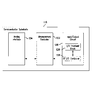
[0082] FIG. 5 is a block diagram illustrating the main functional blocks of
the circuitry of
sensor 100 according to an embodiment in which the circuitry is fabricated in
the
semiconductor substrate 116. In the embodiment illustrated in the FIG. 5, the
circuitry
fabricated in the semiconductor substrate 116 may include an input/output
(I/0) circuit 530,
measurement controller 532 and analog interface 534. The 1/0 circuit 530 may
include an
I/0 frontend block 536 and an I/O controller 538.
[0083] FIG. 6 is block diagram illustrating in more detail the functional
blocks of the
circuitry of sensor 100 according to a non-limiting embodiment in which the
circuitry is
fabricated in the semiconductor substrate 116. As shown in the embodiment of
FIG. 6, in
some embodiments, the 1/0 frontend block 536 of the I/0 circuit 530 may be
connected to the
external inductive element 114, which may be in the form of a coil 220,
through coil contacts
428a and 428b. The 1/0 frontend block 536 may include a rectifier 640, a data
extractor 642,
a clock extractor 644, clamp/modulator 646 and/or frequency divider 648. Data
extractor
642, clock extractor 644 and clamp/modulator 646 may each be connected to
external coil
220 through coil contacts 428a and 428b. The rectifier 640 may convert an
alternating
current produced by coil 220 to a direct current that may be used to power the
sensor 100.
For instance, the direct current may be used to produce one or more voltages,
such as, for
example, voltage VDD_A, which may be used to power the one or more
photodetectors 110.
In one non-limiting embodiment, the rectifier 640 may be a Schottky diode;
however, other
types of rectifiers may be used in other embodiments. The data extractor 642
may extract
data from the alternating current produced by coil 220. The clock extractor
644 may extract a
signal having a frequency (e.g., 13.56MHz) from the alternating current
produced by coil
220. The frequency divider 648 may divide the frequency of the signal output
by the clock
extractor 644. For example, in a non-limiting embodiment, the frequency
divider 648 may be
a 4:1 frequency divider that receives a signal having a frequency (e.g.,
13.56MHz) as an input
27
CA 02861123 2014-07-14
WO 2013/119951
PCT11JS2013/025346
and outputs a signal having a frequency (e.g., 3.39MHz) equal to one fourth
the frequency of
the input signal. The outputs of rectifier 640 may be connected outputs of
rectifier 640 may
be connected to one or more external capacitors 118 (e.g., one or more
regulation capacitors)
through contacts 428h and 428i.
[0084] In some embodiments, the 1/0 controller 538 of the I/O circuit 530
may include a
decoder/serializer 650, command decoder/data encoder 652, data and control bus
654, data
serializer 656 and/or encoder 658. The decoder/serializer 650 may decode and
serialize the
data extracted by the data extractor 642 from the alternating current produced
by coil 220.
The command decoder/data encoder 652 may receive the data decoded and
serialized by the
decoder/serializer 650 and may decode commands therefrom. The data and control
bus 654
may receive commands decoded by the command decoder/data encoder 652 and
transfer the
decoded commands to the measurement controller 532. The data and control bus
654 may
also receive data, such as measurement information, from the measurement
controller 532
and may transfer the received data to the command decoder/data encoder 652.
The command
decoder/data encoder 652 may encode the data received from the data and
control bus 654.
The data serializer 656 may receive encoded data from the command decoder/data
encoder
652 and may serialize the received encoded data. The encoder 658 may receive
serialized
data from the data serializer 656 and may encode the serialized data. In a non-
limiting
embodiment, the encoder 658 may be a Manchester encoder that applies
Manchester
encoding (i.e., phase encoding) to the serialized data. However, in other
embodiments, other
types of encoders may alternatively be used for the encoder 658, such as, for
example, an
encoder that applies 8B/10B encoding to the serialized data.
[0085] The clamp/modulator 646 of the I/0 frontend block 536 may receive
the data
encoded by the encoder 658 and may modulate the current flowing through the
inductive
element 114 (e.g., coil 220) as a function of the encoded data. In this way,
the encoded data
28
may be transmitted wirelessly by the inductive element 114 as a modulated
electromagnetic
wave. The wirelessly transmitted data may be detected by an external reading
device by, for
example, measuring the current induced by the modulated electromagnetic wave
in a coil of
the external reading device. Furthermore, by modulating the current flowing
through the coil
220 as a function of the encoded data, the encoded data may be transmitted
wirelessly by the
coil 220 as a modulated electromagnetic wave even while the coil 220 is being
used to
produce operating power for the sensor 100. See, for example, U.S. Pat Nos.
6,330,464 and
8,073,548, which describe a
coil used to provide operative power to an optical sensor and to wirelessly
transmit data from
the optical sensor. In some embodiments, the encoded data is transmitted by
the sensor 100
using the clamp/modulator 646 at times when data (e.g., commands) are not
being received
by the sensor 100 and extracted by the data extractor 642. For example, in one
non-limiting
embodiment, all commands may be initiated by an external sensor reader (e.g.,
sensor 1500
of FIG. 15) and then responded to by the sensor 100 (e.g., after or as part of
executing the
command). In some embodiments, the communications received by the inductive
element
114 and/or the communications transmitted by the inductive element 114 my be
radio
frequency (RF) communications. Although, in the illustrated embodiments, the
sensor 100
includes a single coil 220, alternative embodiments of the sensor 100 may
include two or
more coils (e.g., one coil for data transmission and one coil for power and
data reception).
[0086] In an embodiment, the I/O controller 538 may also include a
nonvolatile storage
medium 660. In a non-limiting embodiment, the nonvolatile storage medium 660
may be an
electrically erasable programmable read only memory (EEPROM). However, in
other
embodiments, other types of nonvolatile storage media, such as flash memory,
may be used.
The nonvolatile storage medium 660 may receive write data (i.e., data to be
written to the
nonvolatile storage medium 660) from the data and control bus 654 and may
supply read data
29
CA 2861123 2019-06-06
CA 02861123 2014-07-14
WO 2013/119951
PCT11JS2013/025346
(i.e., data read from the nonvolatile storage medium 660) to the data and
control bus 654. In
some embodiments, the nonvolatile storage medium 660 may have an integrated
charge
pump and/or may be connected to an external charge pump. In some embodiments,
the
nonvolatile storage medium 660 may store identification information (i.e.,
traceability or
tracking information), measurement information and/or setup parameters (i.e.,
calibration
information). In one embodiment, the identification information may uniquely
identify the
sensor 100. The unique identification information may, for example, enable
full traceability
of the sensor 100 through its production and subsequent use. In one
embodiment, the
nonvolatile storage medium 660 may store calibration information for each of
the various
sensor measurements.
[0087] In some embodiments, the analog interface 534 may include a light
source driver
662, analog to digital convel ter (ADC) 664, a signal multiplexer (MUX) 666
and/or
comparator 668. In a non-limiting embodiment, the comparator 668 may be a
transimpedance amplifier, in other embodiments, different comparators may be
used. The
analog intel face 534 may also include light source 108, one or more
photodetectors 110 (e.g.,
first and second photodetectors 224 and 226) and/or a temperature transducer
670. In a non-
limiting, exemplary embodiment, the temperature transducer 670 may be a band-
gap based
temperature transducer. However, in alternative embodiments, different types
of temperature
transducers may be used, such as, for example, thermistors or resistance
temperature
detectors. Furthermore, like the light source 108 and one or more
photodetectors 110, in one
or more alternative embodiments, the temperature transducer 670 may be mounted
on
semiconductor substrate 116 instead of being fabricated in semiconductor
substrate 116.
[0088] The light source driver 662 may receive a signal from the
measurement controller
controller 532 indicating the light source current at which the light source
108 is to be driven,
and the light source driver 662 may drive the light source 108 accordingly.
The light source
CA 02861123 2014-07-14
WO 2013/119951 PCT11JS2013/025346
108 may emit radiation from an emission point in accordance with a drive
signal from the
light source driver 662. The radiation may excite indicator molecules 104
distributed
throughout a matrix layer 106 coated on at least part of the exterior surface
of the sensor
housing 102. The one or more photodetectors 110 (e.g., first and second
photodetectors 224
and 226) may each output an analog light measurement signal indicative of the
amount of
light received by the photodetector. For instance, in the embodiment
illustrated in FIG. 6, the
first photodetector 224 may output a first analog light measurement signal
indicative of the
amount of light received by the first photodetector 224, and the second
photodetector 226
may output a first analog light measurement signal indicative of the amount of
light received
by the second photodetector 226. The comparator 668 may receive the first and
second
analog light measurement signals from the first and second photodetectors 224
and 226,
respectively, and output an analog light difference measurement signal
indicative of the
difference between the first and second analog light measurement signals. The
temperature
transducer 670 may output an analog temperature measurement signal indicative
of the
temperature of the sensor 100. The signal MUX 666 may select one of the analog
temperature measurement signal, the first analog light measurement signal, the
second analog
light measurement signal and the analog light difference measurement signal
and may output
the selected signal to the ADC 664. The ADC 664 may convert the selected
analog signal
received from the signal MUX 666 to a digital signal and supply the digital
signal to the
measurement controller 532. In this way, the ADC 664 may convert the analog
temperature
measurement signal, the first analog light measurement signal, the second
analog light
measurement signal and the analog light difference measurement signal to a
digital
temperature measurement signal, a first digital light measurement signal, a
second digital
light measurement signal and a digital light difference measurement signal,
respectively, and
may supply the digital signals, one at a time, to the measurement controller
532.
31
CA 02861123 2014-07-14
WO 2013/119951
PCT11JS2013/025346
[0089] In some embodiments, the analog interface 534 may also include a
backscatter
functionality. For example, in one embodiment, the backscatter functionality
may be
implemented by impedance modulation through a loosely coupled transformer. The
impedance may be modulated by changing the power loading of circuitry in the
sensor 100.
[0090] In some embodiments, the circuitry of sensor 100 fabricated in the
semiconductor
substrate 116 may additionally include a clock generator 671. The clock
generator 671 may
receive, as an input, the output of the frequency divider 648 and generate a
clock signal CLK.
The clock signal CLK may be used by one or more components of one or more of
the I/0
fronted block 536, I/0 controller 538, measurement controller 532 and analog
interface 534.
In a non-limiting embodiment, the clock signal CLK may have a frequency of
1.13 MHz, but,
in other embodiments, other frequencies may be used.
[0091] In a non-limiting embodiment, data (e.g., decoded commands from the
command
decoder/data encoder 652 and/or read data from the nonvolatile storage medium
660) may be
transferred from the data and control bus 654 of the I/O controller 538 to the
measurement
controller 532 via transfer registers and/or data (e.g., write data and/or
measurement
information) may be transferred from the measurement controller 532 to the
data and control
bus 654 of the I/0 controller 538 via the transfer registers.
[0092] In some embodiments, the circuitry of sensor 100 may include a field
strength
measurement circuit. In embodiments, the field strength measurement circuit
may be part of
the input/output circuit 530 or the measurement controller 532 or may be a
separate
functional component. The field strength measurement circuit may measure the
received
(i.e., coupled) power (e.g., in mWatts). The field strength measurement
circuit may detect
whether the received power is sufficient to run the sensor 100. For example,
the field
strength measurement circuit may detect whether the received power is
sufficient to produce
a certain voltage and/or current. In one non-limiting embodiment, the field
strength
32
CA 02861123 2014-07-14
WO 2013/119951 PCT11JS2013/025346
measurement circuit may detect whether the received power produces a voltage
of at least
approximately 3V and a current of at least approximately 0.5mA. However, other
embodiments may detect that the received power receives produces at least a
different
voltage and/or at least a different current.
[0093] FIG. 7 illustrates the layout of a semiconductor substrate 116
according to an
embodiment of the present invention. In the embodiment shown in FIG. 7, first
and second
photodetectors 224 and 226 are fabricated in the semiconductor substrate 116,
and the
semiconductor substrate 116 has light source mounting pads 772 and 774 for
mounting light
source 108. In one embodiment, light source mounting pads 772 and 774 may
connect to the
anode and cathode, respectively, of a light source 108 mounted on the
semiconductor
substrate 116. In FIG. 7, the input/output (110) circuit 530, measurement
controller 532 and
analog interface 534 (other than first and second photodetectors 224 and 226
and light source
108) is shown as circuitry 776. In the embodiment shown in FIG. 7, the
circuitry 776 is
fabricated in the semiconductor substrate 116.
[0094] In non-limiting embodiments, the semiconductor substrate 116 may
include an
isolation trough 778. The isolation trough 778 may isolate and electrically
separate the first
and second photodetectors 224 and 226. In one embodiment, the isolation trough
778 may be
formed on a center line running between the first and second photodetectors
224 and 226.
Also, in some embodiments, the light source mounting pads 772 and 774 may be
configured
such that the emission point of light source 108, when mounted on the light
source mounting
pads 772 and 774, is aligned on the center line running between the first and
second
photodiodes 224 and 226. Similarly, in some embodiments in which the light
source 108 is
fabricated in the silicon substrate 116, the emission point of the fabricated
light source 108 is
aligned on the center line running between the first and second photodiodes
224 and 226. In
some embodiments, the fabrication of symmetrical photodetectors 224 and 226
(i.e.,
33
CA 02861123 2014-07-14
WO 2013/119951 PCT11JS2013/025346
photodetectors which are symmetrical relative to the light source emission
point) may realize
dual channels that are closer to being identical to each other than can be
achieved by using
discrete parts (e.g., photodetectors mounted on the semiconductor substrate
116). The nearly
identical photodetector channels may improve the accuracy of the sensor
measurements.
This may be especially true when, in some embodiments, the nearly identical
dual
photodetector channels are utilized as a signal channel and a reference
channel, respectively.
[0095] The layout of the first and second photodetectors 224 and 226 on
silicon substrate
116 is not limited to the embodiment illustrated in FIG. 7. Other embodiments
may use
different photodetector layouts, such as, for example, those shown in FIGS. 8
and 9. FIG. 8
illustrates an embodiment of the silicon substrate 116 in which the
photosensitive areas of the
first and second photodetectors 224 and 226 do not extend all the way between
the light
source mounting pads 772 and 774. FIG. 9 illustrates an embodiment of the
silicon substrate
116 in which the photosensitive areas of the first and second photodetectors
224 and 226 do
not extend above and below the light source mounting pads 772 and 774.
[0096] FIG. 10 illustrates the layout of the light source mounting pads 772
and 774 on
silicon substrate 116 according to one embodiment of the silicon substrate
116. The light
source mounting pads 772 and 774 may be flip-chip LED mounting pads configured
for
mounting of a flip-chip mounted LED, and light source 108 may be a flip-chip
mounted
LED, such as, for example, the flip-chip mounted LED 1180 illustrated in the
cross-sectional
view in FIG. 11. As shown in the FIG. 11, flip-chip mounted LED 1180 may have
an anode
1182, a cathode 1184, a cover layer 1186, a transparent electrode 1188, a p-
type
semiconductor (e.g., Gallium Nitride (GaN)) layer 1190, an n-type
semiconductor (e.g., GaN)
layer 1192, a substrate (e.g., sapphire substrate) layer 1194 and/or a
backside metal (e.g., a
gold tin alloy (Au-Sn)) layer 1196. FIG. 12 is a bottom view of the flip-chip
mounted LED
1180 shown in FIG. 11 and illustrates the anode 1182 and cathode 1184, which
connect to
34
CA 02861123 2014-07-14
WO 2013/119951
PCT/1JS2013/025346
light source mounting pads 772 and 774 when the flip-chip mounted LED 1180 is
mounted
on the silicon substrate 116.
[0097] Although FIG. 10 illustrates the layout of the light source mounting
pads 772 and
774 according to the one embodiment, other embodiments may use other layouts,
including
other flip-chip LED mounting pad layouts. For example, FIG. 13 illustrates the
layout of the
light source mounting pads 772 and 774 on silicon substrate 116 according to
one possible
alternative embodiment of the silicon substrate 116. Moreover, the silicon
substrate 116 may
be implemented with different light source mounting pad layouts for connecting
to the
different anode and cathode layouts of different light sources.
[0098] In some embodiments, the silicon substrate 116 may be configured to
support one
or more internal photodetectors 110 (i.e., one or more photodetectors
fabricated in the
semiconductor substrate 116) and one or more external photodiodes 110. FIG. 14
illustrates
an exemplary embodiment of the functional blocks of circuitry fabricated on a
silicon
substrate 116 configured to support first and second internal photodetectors
224a and 226a
and first and second external photodetectors 224b and 226b. Relative to the
embodiment
illustrated in FIG. 6, the analog interface 534 of the embodiment of the
functional blocks of
circuitry fabricated on a silicon substrate 116 illustrated in FIG. 14 may
additionally include
an input multiplexor (MUX) 1498. The input MUX 1498 may selectively provide
either the
outputs of first and second internal photodetectors 224a and 226a or the
outputs of the first
and second external photodetectors 224b and 226b as outputs to the comparator
668 and/or
signal MUX 666.
[0099] FIG. 15 illustrates an example of a sensor system including sensor
100 and a
sensor reader 1500 according to one embodiment of the present invention. In
the
embodiment shown in FIG. 15, the sensor 100 may be implanted, for example,
near a
patient's wrist. For example, as shown in FIG. 15, in one non-limiting
embodiment, the
CA 02861123 2014-07-14
WO 2013/119951 PCT11JS2013/025346
sensor 100 may be implanted between the skin 1502 and subcutaneous tissues
1504. In a
non-limiting embodiment, the reader 1500 may be worn like a watch on the
patient's arm.
That is, the reader 1500 may be attached to a wristband 1506. In some
embodiments, the
reader 1500 may be combined with a conventional watch. In a non-limiting
embodiment, the
wristband 1506 is an opaque wristband that may reduce the amount of ambient
light that
reaches the implanted sensor 100. However, in other embodiments, the reader
1500 may not
be worn or otherwise attached to the patient, and the patient may simply bring
the sensor 100
into proximity of the reader 1500 by bringing the reader 1500 near the
patient's wrist.
Furthermore, in some embodiments, the sensor 100 may be implanted in a part of
the
patient's body other than near the patient's wrist, such as, for example, in
the abdomen or an
upper part of the arm.
[00100] In some embodiments, the sensor reader 1500 may include a transceiver
1508, a
processor 1510 and/or a user interface 1512. In one embodiment, the user
interface 1512
may include a liquid crystal display (LCD), but, in other embodiments,
different types of
displays may be used. In some embodiments, the transceiver 1508 may include an
inductive
element, such as, for example, a coil. The transceiver 1508 may generate an
electromagnetic
wave (e.g., by using a coil) to induce a current in the inductive element 114
of the sensor 100,
which powers the sensor 100. The transceiver 1508 may also transmit data
(e.g., commands)
to the sensor 100. For example, in a non-limiting embodiment, the transceiver
1508 may
transmit data by modulating the generated electromagnetic wave used to power
the sensor
100 (e.g., by modulating the current flowing through a coil of the transceiver
1508). As
described above, the modulation in the electromagnetic wave generated by the
reader 1500
may be detected/extracted by the sensor 100 (e.g., by data extractor 642).
Moreover, the
transceiver 1508 may receive data (e.g., measurement information) from the
sensor. For
example, in a non-limiting embodiment, the transceiver 1508 may receive data
by detecting
36
modulations in the electromagnetic wave generated by the sensor 100 (e.g., by
clamp/modulator 646), e.g. , by detecting modulations in the current flowing
through the coil
of the transceiver 1508.
[00101] In some embodiments, the processor 1510 may output to the transceiver
1508 the
data to be transmitted to the sensor 100 and may receive from the transceiver
1508 the data
received from the sensor 100. In one embodiment, the processor 1510 may
serialize and
encode the data to be transmitted to the sensor 100 before outputting it to
the transceiver 1508
for transmission. Similarly, the processor 1510 may decode and/or serialize
the data received
from the sensor 100. In some embodiments, the data received from the sensor
100 may be
measurement information, and the processor 1510 may process the measurement
information
to determine a concentration of an analyte. However, in other embodiments, the
sensor 100
may process the measurement information to determine a concentration of an
analyte, and the
data received from the sensor 100 may be the determined concentration of the
analyte. In
SO= embodiments, the processor 1510 may cause the user interface 1512 to
display a value
representing the concentration of the analyte so that a user (e.g., the
patient, a doctor and/or
others) can read the value. Also, in some embodiments, the processor 1510 may
receive from
the user interface 1512 user input (e.g., a user request for a sensor reading,
such as the
concentration of an analyte).
[00102] In some embodiments, the sensor reader 1500 may include one or more
photodetectors. In one embodiment, the sensor reader 1500 may use the one or
more
photodetectors to detect ambient light, and, if to much light is detected,
issue a warning to the
user via user interface 1512. In some embodiments, the system including sensor
reader 1500
and sensor 100 may incorporate the methods for ambient light detection and
warning
issuance described in U.S. Patent No. 7,157,723. Furthermore, in some
embodiments, the sensor
reader 1500 may include one or
37
CA 2861123 2019-06-06
CA 02861123 2014-07-14
WO 2013/119951 PCT11JS2013/025346
more input/output ports that enable transmission of data (e.g., traceability
information and/or
measurement information) and receipt of data (e.g., sensor commands and/or
setup
parameters) between the sensor reader 1500 and another device (e.g., a
computer).
[00103] In some embodiments, such as, for example, those illustrated FIGS. 7-
9, where the
circuitry 776 and first and second photodetectors 224 and 226 may be
fabricated in
semiconductor substrate 116, the semiconductor substrate 116 may provide a
custom
integrated circuit that merges full functionality for an optical sensor
interface onto a single
chip that needs only minimal connections to external passive components (e.g.,
capacitors
118) and/or a light source 108 (e.g., LED). In fact, in some embodiments, the
number of
external components of sensor 100 connected to the circuitry fabricated the
semiconductor
substrate 116 may be reduced to five or fewer (e.g., one or more capacitors
118, inductive
element 114 and/or light source 108). Furthermore, in some embodiments, the
light source
108 may also be fabricated in the semiconductor substrate 116. The reduced
external
component count and associated reduction in the number of connections may
contribute to
improved sensor robustness and/or to reduce manufacturing complexity.
[00104] According to aspects of the present invention, the circuitry
fabricated in
semiconductor substrate 116, which may include one or more photodetectors 110
and/or light
source 108, may provide an optical transduction along with the ability to
receive and transmit
data through a remotely powered, wireless interface. In other words, the
functionality of
sensor 100 may include remote powering and bi-directional wireless data
communication.
The circuitry fabricated in semiconductor substrate 116 may have the ability
to check the
received power through its remotely powered interface as well as check that
the regulated
voltages are sufficient to supply power to all of the blocks.
[00105] As explained above, in some embodiments of the present invention, the
circuitry
fabricated in semiconductor substrate 116 may also have the ability to execute
diagnostic
38
CA 02861123 2014-07-14
WO 2013/119951 PCT11JS2013/025346
measurements that check the integrity of various blocks (e.g., comparator 668
and/or ADC
664) in the analog front end (e.g., analog interface 534) of the chip. The one
or more
photodetectors 110 may provide the light to current transduction, which may be
processed
further through the integrated comparator (e.g., transimpedance amplifier) 668
and ADC 664.
The analog interface 534 may also have a temperature transducer 670, which, in
some
embodiments, may be an integrated, band-gap based temperature sensor. In some
embodiments, the temperature transducer 670 may provide temperature as an
independent
measurement and/or for optical or system compensation since (e.g., in one
embodiment) the
output of the temperature transducer 670 may be processed along with the
fluorescence
information received through the one or more photodetectors 110.
[00106] In some embodiments, the analog interface 534, acting under the
control of the
measurement controller 532, may execute a measurement sequence (e.g.,
measurement
command execution process 1700, which is described below with reference to
FIGS. 17 and
18) and then report the results to the sensor reader 1500. In one embodiment,
the
measurement sequence may be a pre-loaded sequence (i.e., a pre-stored timing
sequence). In
some embodiments, the measurement sequence may have multiple time slots for
one or more
measurements from first photodetector 224, one or more measurements from
second
photodetector 226, one or more difference measurements comparing the currents
from first
and second photodetectors 224 and 226, one or more temperature measurements of
the silicon
substrate 116 and/or sensor 100, one or more field current measurements (i.e.,
measurements
of the incident power received through the inductive element 114), one or more
excitation
current source regulation measurements (i.e., measurements to check that the
light source 108
is in regulation), one or more voltage measurements and/or one or more
diagnostic
measurements to ensure proper functionality of the various component blocks of
the analog
39
CA 02861123 2014-07-14
WO 2013/119951
PCT11JS2013/025346
interface 543. In various embodiments, the sensor 100 may be used for
continuous readout
and/or power up on demand for a remotely queried measurement.
[00107] In some embodiments, each of these measurements may be digitized
through
ADC 664, which may also be fabricated in the semiconductor substrate 116.
Because the
ADC 664 may convert one or more analog measurements to digital measurements,
in some
embodiments, the bi-directional wireless data communication may be bi-
directional, digital
wireless data communication. Digital data communication may have an improved
signal
integrity relative to analog data communication, and, in some embodiments, the
sensor 100
may utilize solely digital data communication as opposed analog data
communication. In a
non-limiting embodiment, all or a portion of the data is transmitted according
to a known
protocol that includes a checksum.
[00108] FIG. 16 illustrates an exemplary sensor control process 1600 that may
be
pea formed by the optical sensor 100, which may be, for example, implanted
within a living
animal (e.g., a living human), in accordance with an embodiment of the present
invention.
The sensor control process 1600 may begin with a step 1602 of wirelessly
receiving one or
more commands and power. In one embodiment, the power may be in the form of a
modulated electromagnetic wave the sensor 100 may receive. The modulated
electromagnetic wave may induce a current in inductive element 114, and the
input/output
circuit 530 may convert the induced current into power for operating the
sensor 100 and
extract and decode commands from the induced current. In a non-limiting
embodiment,
rectifier 640 may be used to convert the induced current into operating power
for the sensor
100, data extractor 642 may extract data from the current induced in inductive
element 114,
decoder/serializer 650 may decode and serialize the extracted data, and
command
decoder/data encoder 652 may decode one or more commands from the decoded and
serialized extracted data. The one or more decoded commands may then be sent
to
CA 02861123 2014-07-14
WO 2013/119951 PCT11JS2013/025346
measurement controller 532 via the data and control bus 654. In some
embodiments, the one
or more commands and power received by the sensor 100 may be transmitted by
the
transceiver 1508 of sensor reader 1500.
[00109] In step 1604, the optical sensor 100 may execute the received command.
For
example, in one embodiment, the optical sensor 100 may execute the received
command
under control of the measurement controller 532. Example command execution
processes
that may be performed by the optical sensor 100 in step 1602 to execute the
received
commands are described below with reference to FIGS. 17-20.
[00110] Examples of commands that may be received and executed by the sensor
100 may
include measurement commands, get result commands and/or get traceability
information
commands. Examples of measurement commands may include measure sequence
commands
(i.e., commands to perform a sequence of measurements, and after finishing the
sequence,
transmitting the resulting measurement information), measure and save commands
(i.e.,
commands to perform a sequence of measurements and, after finishing the
sequence, saving
the resulting measurement information without transmitting the resulting
measurement
information) and/or single measurement commands (i.e., commands to perform a
single
measurement). The single measurement commands may be commands to save and/or
transmit the measurement information resulting from the single measurement.
The
measurement commands may or may not include setup parameters (i.e.,
calibration
information). Measurement commands that do not have setup parameters may, for
example,
be executed using stored setup parameters (e.g., in nonvolatile storage medium
660). Other
measurement commands, such as measurement commands to both save and transmit
the
resulting measurement information, are possible. The commands that may be
received and
executed by the sensor 100 may also include commands to update the stored the
setup
parameters. The examples of commands described above are not exhaustive of all
commands
41
CA 02861123 2014-07-14
WO 2013/119951 PCT11JS2013/025346
that may be received and executed by the sensor 100, which may be capable of
receiving and
executing one or more of the commands listed above and/or one or more other
commands.
[00111] FIG. 17 illustrates a measurement command execution process 1700 that
may be
performed in step 1604 of the sensor control process 1600 by the optical
sensor 100 to
execute a measurement command received by the optical sensor 100 in accordance
with an
embodiment of the present invention. The measurement command execution process
1700
may begin with a step 1702 of deteimining whether the wirelessly received
power is
sufficient to execute the received measurement command. In other words, in
step 1702, the
sensor 100 may determine whether the electromagnetic field or wave that may
induce a
current in inductive element 114 is strong enough to generate sufficient
operating power for
execution of the received measurement command, which, as described below, may
include
using light source 108 to irradiate indicator molecules 104. In one
embodiment, step 1702
may be performed by a field strength measurement circuit, which may be part of
the
measurement controller 532 or may be a separate component of the circuitry 776
on the
silicon substrate 116.
[00112] In some embodiments, if the sensor 100 determines in step 1702 that
the
wirelessly received power is insufficient to execute the received measurement
command, the
measurement command execution process 1700 may proceed to a step 1704 in which
the
sensor 100 may transmit (e.g., by way of the input/output circuit 530 and
inductive element
114) data indicating that that the wirelessly received power is insufficient
to execute the
received measurement command. In some embodiments, the insufficient power data
may
merely indicate that the power is insufficient, but in other embodiments, the
insufficient
power data may indicate the percentage of the power needed to execute the
received
measurement command that is currently being received.
42
CA 02861123 2014-07-14
WO 2013/119951 PCT11JS2013/025346
[00113] In one embodiment, upon detection that the received power is
insufficient, the
measurement controller 532 may output insufficient power data to the data and
control bus
654. The data and control bus 654 may transfer the insufficient power data to
the command
decoder/data encoder 652, which may encode the insufficient power data. The
data serializer
656 may serialize the encoded insufficient power data. The encoder 658 may
encode the
serialized insufficient power data. The clamp/modulator 646 may modulate the
current
flowing through the inductive element 114 (e.g., coil 220) as a function of
the encoded
insufficient power data. In this way, the encoded insufficient power data may
be transmitted
wirelessly by the inductive element 114 as a modulated electromagnetic wave.
In some
embodiments, the encoded insufficient power data wirelessly transmitted by the
sensor 100
may be received by the sensor reader 1500, which may display a message on user
interface
1512 a message indicating that the power received by the sensor 100 is
insufficient and/or the
extent to which the received power is insufficient.
[00114] In some embodiments, if the sensor 100 determines in step 1702 that
the
wirelessly received power is sufficient to execute the received measurement
command, the
measurement command execution process 1700 may proceed to a step 1706 in which
a
measurement and conversion process may be performed. The measurement and
conversion
process may, for example, be performed by the analog interface 534 under
control of the
measurement controller 532. In one embodiment, the measurement and conversion
sequence
may include generating one or more analog measurements (e.g., using one or
more of
temperature transducer 670, light source 108, first photodetector 224, second
photodetecor
226 and/or comparator 668) and converting the one or more analog measurements
to one or
more digital measurements (e.g., using ADC 664). One example of the
measurement
conversion process that may be performed in step 1706 is described in further
detail below
with reference to FIG. 18.
43
CA 02861123 2014-07-14
WO 2013/119951 PCT11JS2013/025346
[00115] At step 1708, the optical sensor 100 may generate measurement
information in
accordance with the one or more digital measurements produced during the
measurement and
conversion sequence performed in step 1706. Depending on the one or more
digital
measurements produced in step 1706, the measurement information may be
indicative of the
presence and/or concentration of an analyte in a medium in which the sensor
100 is
implanted. In one embodiment, in step 1706, the measurement controller 532 may
receive
the one or more digital measurements and generate the measurement information.
[00116] At step 1710, the optical sensor 100 may determine whether the
measurement
information generated in step 1708 should be saved. In some embodiments, the
measurement
controller 532 may determine whether the measurement information should be
saved. In one
embodiment, the measurement controller 532 may determine whether the
measurement
information should be saved based on the received measurement command. For
example, if
the measurement command is a measure and save command or other measurement
command
that includes saving the resulting measurement information, the measurement
controller 532
may determine that the measurement information generated in step 1708 should
be saved.
Otherwise, if the measurement command is a measure sequence command or other
measurement command that does not include saving the resulting measurement
information,
the measurement controller 532 may determine that the measurement information
generated
in step 1708 should not be saved.
[00117] In some embodiments, if the sensor 100 determines in step 1710 that
the
measurement information generated in step 1708 should be saved, the
measurement
command execution process 1700 may proceed to a step 1712 in which the sensor
100 may
save the measurement information. In one embodiment, after determining that
the
measurement information generated in step 1708 should be saved, the
measurement
controller 532 may output the measurement information to the data and control
bus 654,
44
CA 02861123 2014-07-14
WO 2013/119951 PCT11JS2013/025346
which may transfer the measurement information to the nonvolatile storage
medium 660.
The nonvolatile storage medium 660 may save the received measurement
information. In
some embodiments, the measurement controller 532 may output, along with the
measurement
information, an address at which the measurement information is to be saved in
the
nonvolatile storage medium 660. In some embodiments, the nonvolatile storage
medium 660
may be configured as a first-in-first-out (FIFO) or last-in-first-out (LIFO)
memory.
[00118] In some embodiments, if the sensor 100 determines in step 1710 that
the
measurement information generated in step 1708 should not be saved, or after
saving the
measurement information in step 1712, the measurement command execution
process 1700
may proceed to a step 1714 in which the optical sensor 100 may determine
whether the
measurement information generated in step 1708 should be transmitted. In some
embodiments, the measurement controller 532 may determine whether the
measurement
information should be transmitted. In one embodiment, the measurement
controller 532 may
determine whether the measurement information should be transmitted based on
the received
measurement command. For example, if the measurement command is a measure
sequence
command or other measurement command that includes transmitting the resulting
measurement information, the measurement controller 532 may determine that the
measurement information generated in step 1708 should be transmitted.
Otherwise, if the
measurement command is a measure and save command or other measurement command
that
does not include transmitting the resulting measurement information, the
measurement
controller 532 may determine that the measurement information generated in
step 1708
should not be transmitted.
[00119] In some embodiments, if the sensor 100 determines in step 1714 that
the
measurement information generated in step 1708 should be transmitted, the
measurement
command execution process 1700 may proceed to a step 1716 in which the sensor
100 may
CA 02861123 2014-07-14
WO 2013/119951 PCT11JS2013/025346
transmit the measurement information. In one embodiment, after determining
that the
measurement information generated in step 1708 should be transmitted, the
measurement
controller 532 may output the measurement information to the data and control
bus 654. The
data and control bus 654 may transfer the measurement information to the
command
decoder/data encoder 652, which may encode the measurement information. The
data
serializer 656 may serialize the encoded measurement information. The encoder
658 may
encode the serialized measurement information. The clamp/modulator 646 may
modulate the
current flowing through the inductive element 114 (e.g., coil 220) as a
function of the
encoded measurement information. In this way, the encoded measurement
information may
be transmitted wirelessly by the inductive element 114 as a modulated
electromagnetic wave.
In some embodiments, the encoded measurement information wirelessly
transmitted by the
sensor 100 may be received by the sensor reader 1500, which may display a
value
representing the concentration of the analyte so that a user (e.g., the
patient, a doctor and/or
others) can read the value.
[00120] In some embodiments, after the sensor 100 (a) transmitted insufficient
power data
in step 1704, (b) determined in step 1714 that the measurement information
generated in step
1708 should not be transmitted or (c) transmitted measurement information in
step 1716, the
measurement command execution process 1700 that may be performed in step 1604
of the
sensor control process 1600 by the optical sensor 100 to execute a measurement
command
received by the optical sensor 100 may be completed, and, at this time, the
sensor control
process 1600 may return to step 1602.
[00121] FIG. 18 illustrates a measurement and conversion process 1800, which
is an
example of the measurement and conversion process that may be performed in
step 1706 of
the measurement command execution process 1700, in accordance with an
embodiment of
the present invention.
46
CA 02861123 2014-07-14
WO 2013/119951 PCT11JS2013/025346
[00122] At step 1802, the sensor 100 may load setup parameters (i.e.,
calibration
information) for performing one or more measurements in accordance with the
received
measurement command. For example, in one embodiment, the measurement
controller 532
may load one or more setup parameters by setting up one or more components
(e.g., light
source 108, first photodetector 224, second photodetector 226, comparator 668
and/or
temperature transducer 534) of the analog interface 534 with the setup
parameters. In some
embodiments, the nonvolatile storage medium 660 may store saved setup
parameters.
Further, as noted above, in some embodiments, the measurement commands may or
may not
include setup parameters. In a non-limiting embodiment, if the measurement
command
includes one or more setup parameters, the measurement controller 532 may
setup one or
more components of the analog interface 534 with the setup parameters with the
one or more
setup parameters included in the measurement command. However, if the
measurement
command does not include one or more setup parameters, the measurement
controller 532
may obtain saved setup parameters stored in the nonvolatile storage medium 660
and setup
one or more components of the analog interface 534 with the saved setup
parameters obtained
from the nonvolatile storage medium 660.
[00123] At step 1804, the sensor 100 may determine whether to execute a single
measurement or a measurement sequence. In some embodiments, the measurement
controller 532 may make the single measurement vs. measurement sequence
determination
by referring to the received measurement command (i.e., is the measurement
command to
execute a single measurement or to execute a measurement sequence`?). For
example, in
some embodiments, if the measurement command is a measure sequence command, a
measure and save command or other command for a measurement sequence, the
measurement controller 532 may determine that a measurement sequence should be
executed.
47
CA 02861123 2014-07-14
WO 2013/119951
PCT11JS2013/025346
However, if the measurement command is a single measurement command, the
measurement
controller 532 may determine that a single measurement should be executed.
[00124] In some embodiments, if the sensor 100 determines in step 1804 that a
measurement sequence should be performed, the sensor 100 may pea __ form
measurement and
conversion sequence steps 1806-1820 of measurement and conversion process
1800.
However, in other embodiments, the sensor 100 may perform a portion of
measurement and
conversion sequence steps 1806-1820 and/or additional measurement and
conversion
sequence steps.
[00125] At step 1806, the sensor 100 may perform a light source bias
measurement and
conversion. For example, in some embodiments, while the light source 108 is on
(i.e., while
the light source 108, under the control of the measurement controller 532, is
emitting
excitation light and irradiating indicator molecules 104), the analog
interface 534 may
generate an analog light source bias measurement signal. In one embodiment,
the ADC 664
may convert the analog light source bias measurement signal to a digital light
source bias
measurement signal. The measurement controller 532 may receive the digital
light source
bias measurement signal and generate (e.g., in step 1708 of the measurement
command
execution process 1700) the measurement information in accordance with the
received digital
light source bias measurement signal. In a non-limiting embodiment, the analog
interface
534 may generate the analog light source bias measurement signal by sampling
the voltage
and the current in the output of the current source that feeds the light
source 108.
[00126] At step 1808, the sensor 100 may perform a light source-on temperature
measurement and conversion. For example, in some embodiments, while the light
source 108
is on (i.e., while the light source 108, under the control of the measurement
controller 532, is
emitting excitation light and irradiating indicator molecules 104), the analog
interface 534
may generate a first analog temperature measurement signal indicative of a
temperature of
48
CA 02861123 2014-07-14
WO 2013/119951
PCT11JS2013/025346
the sensor 100. In one embodiment, the temperature transducer 670 may generate
the first
analog temperature measurement signal while the light source 108 is on. The
ADC 664 may
convert the first analog temperature measurement signal to a first digital
temperature
measurement signal. The measurement controller 532 may receive the first
digital
temperature measurement signal and generate (e.g., in step 1708 of the
measurement
command execution process 1700) the measurement information in accordance with
the
received first digital temperature measurement signal.
[00127] At step 1810, the sensor 100 may perform a first photodetector
measurement and
conversion. For example, in some embodiments, while the light source 108 is on
(i.e., while
the light source 108, under the control of the measurement controller 532, is
emitting
excitation light and irradiating indicator molecules 104), the first
photodetector 224 may
generate a first analog light measurement signal indicative of the amount of
light received by
the first photodetector 224 and output the first analog light measurement
signal to the signal
MUX 666. The signal MUX 666 may select the first analog light measurement
signal and,
the ADC 664 may convert the first analog light measurement signal to a first
digital light
measurement signal. The measurement controller 532 may receive the first
digital light
measurement signal and generate (e.g., in step 1708 of the measurement command
execution
process 1700) the measurement information in accordance with the received
first digital light
measurement signal.
[00128] In a non-limiting embodiment, first photodetector 224 may be a part of
a signal
channel, the light received by the first photodetector 224 may be emitted by
indicator
molecules 104 distributed throughout the indicator membrane 106', and the
first analog light
measurement signal may be an indicator measurement.
[00129] At step 1812, the sensor 100 may perform a second photodetector
measurement
and conversion. For example, in some embodiments, while the light source 108
is on (i.e.,
49
CA 02861123 2014-07-14
WO 2013/119951 PCT11JS2013/025346
while the light source 108, under the control of the measurement controller
532 is emitting
excitation light and irradiating indicator molecules 104), the second
photodetector 226 may
generate a second analog light measurement signal indicative of the amount of
light received
by the second photodetector 226 and output the second analog light measurement
signal to
the signal MUX 666. The signal MUX 666 may select the second analog light
measurement
signal and, the ADC 664 may convert the second analog light measurement signal
to a second
digital light measurement signal. The measurement controller 532 may receive
the second
digital light measurement signal and generate (e.g., in step 1708 of the
measurement
command execution process 1700) the measurement information in accordance with
the
received second digital light measurement signal.
[00130] In a non-limiting embodiment, second photodetector 226 may be a part
of a
reference channel, the light received by the second photodetector 226 may be
emitted by
indicator molecules 104 distributed throughout the reference membrane 106",
and the second
analog light measurement signal may be a reference measurement.
[00131] At step 1814, the sensor 100 may perform a difference measurement and
conversion. For example, in some embodiments, while the light source 108 is on
(Le., while
the light source 108, under the control of the measurement controller 532, is
emitting
excitation light and irradiating indicator molecules 104), (i) the first
photodetector 224 may
generate a first analog light measurement signal indicative of the amount of
light received by
the first photodetector 224, and (ii) the second photodetector 226 may
generate a second
analog light measurement signal indicative of the amount of light received by
the second
photodetector 226. The comparator 668 may receive the first and second analog
light
measurement signals and generate an analog light difference measurement signal
indicative
of a difference between the first and second analog light measurement signals.
The
comparator 668 may output the analog light difference measurement signal to
the signal
CA 02861123 2014-07-14
WO 2013/119951 PCT11JS2013/025346
MUX 666. The signal MUX 666 may select the analog light difference measurement
signal
and, the ADC 664 may convert the analog light difference measurement signal to
a digital
light difference measurement signal. The measurement controller 532 may
receive the digital
light difference measurement signal and generate (e.g., in step 1708 of the
measurement
command execution process 1700) the measurement information in accordance with
the
received digital light difference measurement signal.
[00132] In a non-limiting embodiment, first photodetector 224 may be a part of
a signal
channel, second photodetector 226 may be a part of a reference channel, and
the analog light
difference measurement signal may be indicative of the difference in light
emitted by (a)
indicator molecules 104 distributed throughout indicator membrane 106' and
affected by the
concentration of an analyte in the medium in which sensor 100 is implanted,
and (b) indicator
molecules 104 distributed throughout reference membrane 106" and unaffected by
the
concentration of the analyte in the medium in which sensor 100 is implanted.
[00133] At step 1816, the sensor 100 may pel form a second photodetector
ambient
measurement and conversion. For example, in some embodiments, while the light
source 108
is off (i.e., while the light source 108, under the control of the measurement
controller 532 is
not emitting light), the second photodetector 226 may generate a second analog
ambient light
measurement signal indicative of the amount of light received by the second
photodetector
226 and output the second analog ambient light measurement signal to the
signal MUX 666.
The signal MUX 666 may select the second analog ambient light measurement
signal and,
the ADC 664 may convert the second analog ambient light measurement signal to
a second
digital ambient light measurement signal. The measurement controller 532 may
receive the
second digital ambient light measurement signal and generate (e.g., in step
1708 of the
measurement command execution process 1700) the measurement information in
accordance
with the received second digital ambient light measurement signal.
51
CA 02861123 2014-07-14
WO 2013/119951 PCT1US2013/025346
[00134] In a non-limiting embodiment, second photodetector 226 may be a part
of a
reference channel, the light received by the second photodetector 226 may be
emitted by
indicator molecules 104 distributed throughout the reference membrane 106",
and the second
analog ambient light measurement signal may be an ambient reference
measurement.
[00135] At step 1818, the sensor 100 may perform a first photodetector
ambient
measurement and conversion. For example, in some embodiments, while the light
source 108
is off (i.e., while the light source 108, under the control of the measurement
controller 532, is
not emitting light), the first photodetector 224 may generate a first analog
ambient light
measurement signal indicative of the amount of light received by the first
photodetector 224
and output the first analog ambient light measurement signal to the signal MUX
666. The
signal MUX 666 may select the first analog ambient light measurement signal
and, the ADC
664 may convert the first analog ambient light measurement signal to a first
digital ambient
light measurement signal. The measurement controller 532 may receive the first
digital
ambient light measurement signal and generate (e.g., in step 1708 of the
measurement
command execution process 1700) the measurement information in accordance with
the
received first digital ambient light measurement signal.
[00136] In a non-limiting embodiment, first photodetector 224 may be a part of
a signal
channel, the light received by the first photodetector 224 may be emitted by
indicator
molecules 104 distributed throughout the indicator membrane 106', and the
first analog
ambient light measurement signal may be an ambient indicator measurement.
[00137] At step 1820, the sensor 100 may perform a light source-off
temperature
measurement and conversion. For example, in some embodiments, while the light
source 108
is off (i.e., while the light source 108, under the control of the measurement
controller 532, is
not emitting light), the analog interface 534 may generate a second analog
temperature
measurement signal indicative of a temperature of the sensor 100. In one
embodiment, the
52
temperature transducer 670 may generate the second analog temperature
measurement signal
while the light source 108 is off The ADC 664 may convert the second analog
temperature
measurement signal to a second digital temperature measurement signal. The
measurement
controller 532 may receive the second digital temperature measurement signal
and generate
(e.g., in step 1708 of the measurement command execution process 1700) the
measurement
information in accordance with the received second digital temperature
measurement signal.
[00138] Accordingly, in an embodiment in which sequence steps 1806-1820 of
measurement and conversion process 1800 are performed, the measurement
controller 532
may generate measurement information in accordance with (i) the first digital
temperature
measurement signal, (ii) the first digital light measurement signal, (iii) the
second digital light
measurement signal, (iv) the digital light difference measurement signal, (v)
the second
digital temperature measurement signal, (vi) the first digital ambient light
measurement
signal and (vii) the second digital ambient light measurement signal. In a non-
limiting
embodiment, the calculation of the concentration of the analyte perfumed by
the
measurement controller 532 of sensor 100 and/or sensor reader 1500 may include
subtracting
the digital ambient light signals from the corresponding digital light
measurement signals.
The calculation of the concentration of the analyte may also include error
detection. In some
embodiments, the measurement controller 532 may incorporate methods for
attenuating the
effects of ambient light, such as, for example, those described in U.S. Patent
No. 7,227,156.
In some embodiments, the
measurement controller 532 may generate measurement information that merely
comprises
the digital measurement signals received from the analog interface 534.
However, in other
embodiments, the measurement controller 532 may process the digital signals
received from
the analog interface 534 and determine (i.e., calculate and/or estimate) the
concentration of an
53
CA 2861123 2019-06-06
CA 02861123 2014-07-14
WO 2013/119951 PCT11JS2013/025346
analyte in the medium in which the sensor 100 is implanted, and the
measurement
information may, additionally or alternatively, include the determined
concentration.
[00139] In some embodiments, if the sensor 100 determines in step 1804 that a
measurement sequence should be performed, the measurement and conversion
process 1800
may proceed to a step 1822 in which a single measurement and conversion is
performed. In
some embodiments, based on the measurement command received, the single
measurement
and conversion petformed in step 1822 may be any one of the measurements and
conversions
performed in steps 1806-1820. Accordingly, in an example where step 1822 of
the
measurement and conversion process 1800 is performed, the measurement
controller 532
may receive only one digital measurement signal, and the measurement
information
generated by the measurement controller 532 (e.g., in step 1708 of the
measurement
command execution process 1700) may, in one embodiment, simply be the one
digital
measurement signal received by the measurement controller.
[00140] In some embodiments, light source 108 may be turned on before
execution of step
1806 and not turned off until after execution of step 1814. However, this is
not required. For
example, in other embodiments, the light source 108 may be turned on during
measurement
portions of steps 1806-1814 and turned off during the conversion portions of
steps 1806-
1814.
[00141] Furthermore, although FIG. 18 illustrates one possible sequence of the
measurement and conversion process 1800, it is not necessary that steps 1806-
1820 of the
measurement and conversion process 1800 be performed in any particular
sequence. For
example, in one alternative embodiment, light measurement and conversion steps
1806-1814
may be performed in a different order (e.g., 1808, 1812, 1814, 1810, 1806),
and/or ambient
light measurement and conversion steps 1816-1820 may be performed in a
different order
(e.g., 1818, 1820, 1816). In some embodiments, the light source on temperature
54
CA 02861123 2014-07-14
WO 2013/119951 PCT11JS2013/025346
measurement may be used to provide an error flag in each individual
measurement (e.g., by
using a comparator to comparing the light source on temperature measurement to
threshold
value). In another alternative embodiment, ambient light measurement and
conversion steps
1816-1820 may be performed before light measurement and conversion steps 1806-
1814. In
still another alternative embodiment, steps 1806-1820 of the measurement and
conversion
process 1800 may be performed in a sequence in which all of the steps of one
of light
measurement and conversion steps 1806-1814 and ambient light measurement and
conversion steps 1816-1820 are completed before one or more steps of the other
are executed
(e.g., in one embodiment, steps 1806-1820 may be performed in the sequence
1806, 1808,
1810, 1818, 1816, 1812, 1814, 1820).
[00142] FIGS. 21A and 21B illustrate the timing of an exemplary embodiment of
the
measurement and conversion process 1800 described with reference to FIG. 18.
[00143] FIG. 19 illustrates a get result command execution process 1900 that
may be
performed in step 1604 of the sensor control process 1600 by the optical
sensor 100 to
execute a get result command received by the optical sensor 100 in accordance
with an
embodiment of the present invention. The measurement command execution process
1900
may begin with a step 1902 of retrieving saved measurement information. For
example,
retrieved measurement information may be saved during step 1712 of the
measurement
command execution process 1700 shown in FIG. 17. In some embodiments,
measurement
information is saved in the nonvolatile storage medium 660. In response to a
request from
the measurement controller 532, the nonvolatile storage medium 660 may output
saved
measurement information to the data and control bus 654. In some embodiments,
the data
and control bus 654 may transfer the retrieved measurement information to the
measurement
controller 532. However, in alternative embodiments, the data and control bus
654 may
transfer the retrieved measurement information to the command decoder/data
encoder 652
CA 02861123 2014-07-14
WO 2013/119951 PCT11JS2013/025346
without first transferring the retrieved measurement information to the
measurement
controller 532.
[00144] In some embodiments, the nonvolatile storage medium 660 may output to
the data
and control bus 654 the measurement information most recently saved to the
nonvolatile
storage medium 660. In some alternative embodiments, the nonvolatile storage
medium 660
may output to the data and control bus 654 the oldest measurement information
most saved to
the nonvolatile storage medium 660. In other alternative embodiments, the
nonvolatile
storage medium 660 may output to the data and control bus 654 the measurement
information
specifically requested by the measurement controller 532 (e.g., by an address
sent to the
nonvolatile storage medium 660 with a read request).
[00145] After the saved measurement information is retrieved, the get result
command
execution process 1900 may proceed to a step 1904 in which the sensor 100 may
transmit the
retrieved measurement information. In one embodiment, the measurement
controller 532
may output the retrieved measurement information to the data and control bus
654. The data
and control bus 654 may transfer the measurement information to the command
decoder/data
encoder 652, which may encode the retrieved measurement information. The data
serializer
656 may serialize the encoded retrieved measurement information. The encoder
658 may
encode the serialized retrieved measurement information. The clamp/modulator
646 may
modulate the current flowing through the inductive element 114 (e.g., coil
220) as a function
of the encoded retrieved measurement information. In this way, the encoded
retrieved
measurement information may be transmitted wirelessly by the inductive element
114 as a
modulated electromagnetic wave. In some embodiments, the encoded retrieved
measurement
information wirelessly transmitted by the sensor 100 may be received by the
sensor reader
1500.
56
CA 02861123 2014-07-14
WO 2013/119951 PCT11JS2013/025346
[00146] FIG. 20 illustrates a get identification information command execution
process
2000 that may be performed in step 1604 of the sensor control process 1600 by
the optical
sensor 100 to execute a get identification information command received by the
optical
sensor 100 in accordance with an embodiment of the present invention. The get
identification information command execution process 2000 may begin with a
step 2002 of
retrieving stored identification information. In some embodiments,
identification information
is stored in the nonvolatile storage medium 660. In response to a request from
the
measurement controller 532, the nonvolatile storage medium 660 may output
identification
information to the data and control bus 654. In some embodiments, the data and
control bus
654 may transfer the retrieved identification information to the measurement
controller 532.
However, in alternative embodiments, the data and control bus 654 may transfer
the retrieved
identification information to the command decoder/data encoder 652 without
first transferring
the retrieved identification information to the measurement controller 532.
[00147] After the stored identification information is retrieved, the get
identification
information command execution process 2000 may proceed to a step 2004 in which
the
sensor 100 may transmit the retrieved identification information. In one
embodiment, the
measurement controller 532 may output the retrieved identification information
to the data
and control bus 654. The data and control bus 654 may transfer the
identification information
to the command decoder/data encoder 652, which may encode the identification
information.
The data serializer 656 may serialize the encoded identification information.
The encoder
658 may encode the serialized identification information. The clamp/modulator
646 may
modulate the current flowing through the inductive element 114 (e.g., coil
220) as a function
of the encoded retrieved identification information. In this way, the encoded
identification
information may be transmitted wirelessly by the inductive element 114 as a
modulated
57
CA 02861123 2014-07-14
WO 2013/119951 PCT11JS2013/025346
electromagnetic wave. In some embodiments, the encoded identification
information
wirelessly transmitted by the sensor 100 may be received by the sensor reader
1500.
[00148] The sensor 100 may be capable of executing other commands received by
the
sensor. For example, the sensor 100 may perform a setup parameter update
execution
process that may be performed in step 1604 of the sensor control process 1600
by the optical
sensor 100 to execute a command to update setup parameters. In some
embodiments, the
setup parameter update execution process may replace one or more setup
parameters (i.e.,
initialization information) stored in the nonvolatile storage medium 660. In
one embodiment,
upon receiving a command to update setup parameters, the measurement
controller 532 may
output one or more setup parameters received with the command to the data and
control bus
654, which may transfer the setup parameter(s) to the nonvolatile storage
medium 660. The
nonvolatile storage medium 660 may store the received setup parameter(s). In a
non-limiting
embodiment, the received setup parameter(s) may replace one or more setup
parameters
previously stored in the nonvolatile storage medium 660.
[00149] Embodiments of the present invention have been fully described above
with
reference to the drawing figures. Although the invention has been described
based upon
these preferred embodiments, it would be apparent to those of skill in the art
that certain
modifications, variations, and alternative constructions could be made to the
described
embodiments within the spirit and scope of the invention.
58