Note : Les descriptions sont présentées dans la langue officielle dans laquelle elles ont été soumises.
CA 02862893 2014-08-29
DESCRIPTION
Title of Invention
CAPACITOR INPUT TYPE SMOOTHING CIRCUIT
Technical Field
[0001]
The present invention relates to a capacitor input
type smoothing circuit for shaping the pulsating current
formed when converting AC current to DC current.
Background Art
[0002]
In order to convert AC current to DC current of
arbitrary voltage, it is necessary to perform
rectification or step-up and step-down using certain
methods. Since a pulsating current is obtained in the
conversion described above, it is also necessary to smooth
the pulsating current in order to have a smoother waveform
in a bad case.
[0003]
A simple smoothing method that has been used for a
long time is a method of using an electrolytic capacitor
having a large capacity after rectification. By causing
the capacitor to be charged and discharged, a portion of
the valley of the pulsating current is covered by the
1
CA 02862893 2014-08-29
discharging from the capacitor.
[0004]
In recent years, a power factor correction circuit
using a switching technique has been used. This mainly
controls a current flowing through the coil by switching.
In a so-called capacitor input type or condenser input
type smoothing circuit that uses an electrolytic capacitor
having a large capacity, charging until the voltage of the
pulsating current reaches the apex and discharging when
the pulsating voltage is reduced thereafter are repeated.
[0005]
However, since discharging occurs immediately after
charging, electric power of the capacitor is applied in a
time zone in which the voltage drops from the apex of the
voltage of the pulsating current. This is not the
electric power from the AC power supply but is reactive
power. A reduction in the power factor causes many
problems, such as the generation of harmonics. This
becomes a burden on the power transmission and
distribution side. When harmonic current flows
excessively through the power line, a problem, such as
burnout of a condenser inserted in the power line, occurs
in the worst case.
[0006]
As a power factor correction circuit, there is a
2
CA 02862893 2014-08-29
circuit abbreviated as PFC. However, this circuit is
complicated, and power loss due to switching also occurs
since the switching is accompanied. In addition, there is
also a disadvantage in that switching noise is easily
transmitted through the power supply line.
[0007]
Thus, since a capacitor input type is simple, the
number of components is small and the cost is low. On the
other hand, there is a power factor problem. The power
factor can be improved by the PFC circuit, but a
complicated circuit configuration is required and
accordingly the cost is high. In addition, a circuit for
suppressing noise is also required.
[0008]
In addition, related technologies were investigated,
but any related technology corresponding to the so-called
prior art was not found. For example, there is an
invention disclosed in JP-A-2005-19266 that uses a PFC
circuit. The invention includes a transformer having a
power transformation function and a PFC control unit that
causes the transformer to perform the transformation of DC
power by the on/off control of a switching element in
order to suppress a harmonic current. However, there is
almost no relationship with the present invention.
[0009]
3
CA 02862893 2014-08-29
[Patent Citation 1] JP-A-2005-19266
Disclosure of Invention
Technical Problem
[0010]
The present invention has been made in view of the
circumstances described above, and it is an object of the
present invention to embody a capacitor input type
smoothing circuit capable of suppressing electric power at
the time of charging without reducing the power factor if
possible. In addition, it is another object of the
present invention to obtain a configuration, which can be
realized as easily as possible, with a small number of
components, and accordingly, to realize a significant cost
reduction.
Technical Solution
[0011]
In order to solve the aforementioned problem, the
present invention includes a pulsating circuit that
supplies a pulsating voltage to a load when a capacitor is
not discharged and a control circuit that controls
discharging of the capacitor. The control circuit
includes a smoothing circuit, which is connected in
parallel to the pulsating circuit, and a voltage detection
circuit for detecting the voltage. The voltage detection
circuit determines a voltage range to discharge the
4
CA 02862893 2014-08-29
capacitor, and includes a first switch that is turned off
by detecting that the pulsating voltage is in the voltage
range, a second switch that is connected to the first
switch and is turned on when the first switch is turned
off, and a third switch that is connected to the second
switch and is turned on when the second switch is turned
on. When the pulsating voltage is not in the discharge
voltage range of the capacitor, the first switch is turned
on and the second and third switches are turned off so
that capacitor power is not supplied to the load. A
discharge voltage of the capacitor is set within a range
that is slightly higher than a lower limit of a voltage
that the load requires and is not equal to or greater than
the voltage.
[0012]
The basic configuration of the present invention is
a general capacitor input type smoothing circuit. In
addition, a control circuit for controlling the
discharging of the capacitor is included, and the control
circuit includes a smoothing circuit connected in parallel
to the pulsating circuit and a voltage detection circuit
for detecting the voltage.
[0013]
The voltage detection circuit determines a voltage
range to discharge the capacitor, and includes a first
CA 02862893 2014-08-29
switch that is turned off by detecting that the pulsating
voltage is in the voltage range, a second switch that is
connected to the first switch and is turned on when the
first switch is turned off, and a third switch that is
connected to the second switch and is turned on when the
second switch is turned on.
[0014]
When the pulsating voltage is not in the discharge
voltage range of the capacitor, the first switch is turned
on and the second and third switches are turned off so
that the capacitor power is not supplied to the load. The
discharge voltage of the capacitor is set within a range
that is slightly higher than the lower limit of a voltage
that the load requires and is not equal to or greater than
the voltage.
[0015]
More specifically, a capacitor input type smoothing
circuit of the present invention includes a bridge circuit
connected to an AC power supply and a power line connected
to an output end of the bridge circuit. The power line is
branched into three lines to supply rectified electric
power directly to a capacitor input circuit, a voltage
detection circuit, and a load. A first branch line is
used to supply electric power directly to the load when
the capacitor is not discharged. A second branch line is
6
CA 02862893 2014-08-29
used to supply electric power to the capacitor when a
supplied pulsating voltage rises so that the capacitor is
charged. A third branch line is used to divide the
supplied pulsating voltage and supply the divided voltage
to a voltage detection circuit. A backflow prevention
element is disposed in the first branch line leading to
the load and the second branch line leading to the
capacitor. A voltage detection circuit that determines
and detects a voltage range to discharge the capacitor is
provided in the remaining third branch line. The voltage
detection circuit determines a voltage range to discharge
the capacitor, and includes a first switch that is turned
off by detecting that the pulsating voltage is in the
voltage range, a second switch that is connected to the
first switch and is turned on when the first switch is
turned off, and a third switch that is connected to the
second switch and is turned on when the second switch is
turned on. A discharge voltage of the capacitor is set so
that the pulsating voltage matches an operating base
voltage of the first switch.
[0016]
In the present invention, electric power is mainly
supplied from the commercial AC power supply and is
rectified by the bridge circuit, and electric power is
divided into three parts of the pulsating circuit flowing
7
CA 02862893 2014-08-29
directly to the load, the circuit having a capacitor, and
the voltage detection circuit. The pulsating circuit is
connected to the first branch line, the circuit having a
capacitor is connected to the second branch line, and the
voltage detection circuit is connected to the third branch
line.
[0017]
The first branch line is used to supply electric
power directly to the load when the capacitor is not
discharged. The second branch line is used to supply
electric power to the capacitor when a supplied pulsating
voltage rises so that the capacitor is charged. A third
branch line is used to divide the supplied pulsating
voltage and supply the divided voltage to the voltage
detection circuit.
[0018]
By the first branch line to the load, electric power
is directly supplied to the load when the capacitor of the
circuit of the present invention is not discharged. The
capacitor is charged when the voltage of the supplied
pulsating current rises.
[0019]
The voltage detection circuit determines a voltage
range to discharge the capacitor, and includes a first
switch that is turned off by detecting that the pulsating
8
CA 02862893 2014-08-29
voltage is in the voltage range, a second switch that is
connected to the first switch and is turned on when the
first switch is turned off, and a third switch that is
connected to the second switch and is turned on when the
second switch is turned on.
[0020]
In addition, when the voltage detection circuit
detects a voltage range where the capacitor is charged but
no electric power is supplied from the capacitor to the
load, an electronic switch 1 is turned on, and an
electronic switch 2 connected thereto is turned off. In
addition, an electronic switch 3 connected to the
electronic switch 2 is also turned off, and no electric
power is supplied from the capacitor to the load.
[0021]
Preferably, the voltage range to discharge the
capacitor is set within a range that is slightly higher
than the lower limit of a voltage that the load requires
and is lower than the voltage. Simply, it is possible to
use a method of matching the pulsating voltage to the
operating base voltage of the transistor using a dividing
resistor or the like, for example.
Advantageous Effects
[0022]
According to the present invention, electric power
9
CA 02862893 2014-08-29
in a time zone in which the pulsating voltage drops is not
supplied from the power line. Even in the time zone in
which the pulsating voltage drops, the supply of electric
power from the capacitor to the load is stopped by the
voltage detection circuit of the present invention and the
control circuit, and electric power is supplied from the
power line to the load through the bypassed third branch
line. Accordingly, a problem that the power factor is
lowered is solved. That is, a problem, which is a
disadvantage of a simple capacitor input method, is solved
in which, once the voltage of the pulsating current starts
to drop, the capacitor starts to be discharged and
electric power in the time zone in which the pulsating
voltage drops is no longer supplied from the power line,
and accordingly, the power factor is lowered.
[0023]
In addition, by setting the voltage detection
circuit provided in the second branch line so that
electric power is supplied from the capacitor to the load
immediately before reaching the lower limit of the voltage
that the load requires, discharge time is minimized.
Accordingly, it is possible to adopt a smaller capacitor.
Thus, the effect of suppressing the electric power at the
time of charging is also obtained.
[0024]
CA 02862893 2014-08-29
Even in the time zone of a valley of the pulsating
current, discharging of the capacitor starts from a
voltage obtained by subtracting the loss from the maximum
voltage at the time of charging in the circuit of the
present invention. This is useful since power is present.
Switching between electric power from the power line of
the first branch line and electric power from the
capacitor of the second branch line occurs only twice
during one period of the pulsating current. Accordingly,
noise and loss due to the switching are minimized.
[0025]
In particular, since the present invention can be
configured very simply, the number of components is small,
and no expensive components are required. Therefore, it
is possible to significantly reduce the cost compared with
a power factor correction circuit that has been
conventionally common. In addition, by setting the
discharge voltage of the capacitor in a range that is not
equal to or greater than the lower limit of the voltage
that the load requires, the valley of the pulsating
current can be covered with a smaller amount of charging
than a typical capacitor. Therefore, the capacitance of
the capacitor itself can be further reduced, and the power
factor is further improved since the current is low.
Best Mode for Carrying Out the Invention
11
CA 02862893 2014-08-29
[0026]
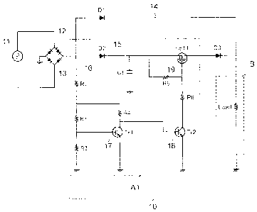
Hereinafter, a capacitor input type smoothing
circuit 10 of the present invention will be described in
detail with reference to an embodiment shown in the
diagrams. Fig. 1 is an example 1 in which rectified
electric power is supplied through a bridge circuit 12,
which is formed by diodes, from a commercial AC power line
that is an AC power supply 11. Since this has not been
smoothed, this is a DC current, but becomes a pulsating
current having a rising voltage (refer to Figs. 2 and 3).
[0027]
The pulsating current has the bridge circuit 12
connected to the AC power supply 11 and a power line 13
connected to the output end of the bridge circuit 12, and
the power line 13 is branched into three lines of a
pulsating circuit 14 to supply the rectified electric
power directly to a load, a smoothing circuit (or a
capacitor input circuit) 15, and a voltage detection
circuit 16.
[0028]
The smoothing circuit (or the capacitor input
circuit) 15 and the voltage detection circuit 16 form a
control circuit Al that controls the discharging of the
capacitor. On the upstream side of the capacitor
connection point of the pulsating circuit 14 and the
12
CA 02862893 2014-08-29
smoothing circuit 15 leading to a load B, diodes are
inserted as backflow prevention elements D1 and D2.
[0029]
Among the three branch lines, the first branch line
is connected to the pulsating circuit 14 that flows
directly to the load through the diode Dl. The second
branch line is connected to the smoothing circuit 15 that
flows to a capacitor Cl through the diode D2. The third
branch line is connected to the voltage detection circuit
16 that is voltage-divided through resistors R1, R2, and
R3 inserted in series in the same order.
[0030]
In the first branch line, when the capacitor Cl is
not discharged, electric power is directly supplied to the
load B from the power line. In the second branch line,
the capacitor Cl is charged when the voltage of the
supplied pulsating current rises. In the third branch
line, the voltage of the supplied pulsating current is
divided by three resistors.
[0031]
The divided voltage between the combined resistance
of the resistors R2 and R3 and the resistor R1 is used to
drive a base of a transistor Tr2 that is a second switch
18. The divided voltage between the combined resistance
of the resistors R1 and R2 and the resistor R3 is set such
13
CA 02862893 2014-08-29
that the discharging of the capacitor 01 is stopped when
reaching a base voltage of Tr1 that is a first switch 17.
[0032]
Resistors R5 and R6 are for generating an
appropriate voltage for driving FET1 that is a third
switch 19. The resistor R6 is inserted in a circuit
connecting the second and third switches 18 and 19 to each
other, and the resistor R5 is inserted between the third
switch 19 and the capacitor Cl of the smoothing circuit 15
and between the resistor R6 and the third switch 19.
[0033]
In the case illustrated, a field effect transistor
(FET) is used as the third switch 19, and the FET1 is Pch
(P channel type). Therefore, a current flows through the
resistor R6 from the gate at the time of power application.
Since the FET can be driven with a small amount of current
in general, there is no burden on the transistor Tr2.
Therefore, the resistor R6 should be set such that too
much current does not flow.
[0034]
As described above, D1, D2, and D3 indicate diodes
for backflow prevention. The diodes D1 and D2 are
necessary to avoid detecting inappropriate voltages due to
backflow power from the capacitor Cl at the time of
voltage detection of electric power from the power line by
14
CA 02862893 2014-08-29
resistors R1, R2, and R3. The diode D3 is inserted in
order to prevent electric power passing through the diode
D1 from flowing to the capacitor Cl through a damage
prevention diode built in the FET1. It should be
remembered that a large amount of current cannot flow
through the damage prevention diode.
[0035]
When a voltage supplied from the commercial AC power
line is AC 210 V. a DC voltage corresponding thereto is
296 V. Assuming that the resistor R1 is 2.2 MQ, the
resistor R2 is 260 KQ, the resistor R3 is 14 KSI, and the
resistor R4 is 260 KC2, the base voltage of the transistor
Trl becomes about 0.56 V at around 180 V. The transistor
Trl is turned on and off with this voltage as a boundary.
[0036]
Therefore, the above can be calculated as follows.
(Combined resistance) 274 KC2 = (R2) 260 KS-2 + (R3) 14
KQ,
(Combined resistance) 133 KK-2 = parallel of 133 KK-2 -
(R2 + R3) 274 KQ and (R4) 260 KQ,
(Combined resistance) 2333 1<0 = (R1) 2200 KQ + 133
KQ.
When the voltage is 180 V, a current flowing through
the resistor R1 is about 80 A - 180 V/2333 1<0.
A current of about 40 A that is approximately half
CA 02862893 2014-08-29
of 80 A flows through the resistors R2 and R4.
A current of about 40 A also flows through the
resistor R3, and the base voltage of the transistor Trl
becomes about 0.56 V = 14 KO x 40 A.
[0037]
In a capacitor input type smoothing circuit 10 of
the present invention having such a configuration, when
the transistor Trl is turned on, the collector voltage of
the transistor Trl drops, and the base voltage of the
transistor Tr2 connected thereto drops. Then, the
transistor Tr2 is turned off. When the transistor Tr2 is
turned off, the voltage of the gate of the Pch FET1
connected to the collector of the transistor Tr2 does not
become a negative potential, and the FET1 is turned off.
Accordingly, discharging from the capacitor Cl to the load
B does not occur.
[0038]
When the transistor Trl is turned off, the collector
voltage of the transistor Trl rises, and the base voltage
of the transistor Tr2 connected thereto also rises. Then,
the transistor Tr2 is turned on. When the transistor Tr2
is turned on, the voltage of the gate of the Pch FET1
connected to the collector of the transistor Tr2 becomes a
negative potential, and the FET1 is turned on.
Accordingly, discharging from the capacitor Cl to the load
16
CA 02862893 2014-08-29
B occurs.
[0039]
In the example 1, the transistor Tr2 is to be turned
off near the pulsating voltage of 0 V. In practice,
however, since there is also a small amount of capacitance
in the base of the transistor as in the FET, the
transistor Tr2 is turned on by the remaining electric
power. The field effect transistor FET1 of the third
switch is turned on even with a weak current. Therefore,
no de facto problem is caused even if the transistor Tr2
of the second switch is semi-open.
[0040]
However, since the completeness of the operation is
also important, it is possible to adopt a configuration
shown in Fig. 2 for the case. In a smoothing circuit of
example 2 according to the present invention shown in Fig.
2, a capacitor 02 having an appropriate capacity is
additionally connected to the collector of the transistor
Trl and the base of the transistor Tr2, so that current
application is ensured. Thus, it is possible to hold the
conduction of the transistor Tr2 near the pulsating
voltage of 0 V. In addition, since the other
configuration of Example 2 including a control circuit A2
is the same as Example 1, detailed explanation thereof
will be omitted.
17
CA 02862893 2014-08-29
[0041]
Fig. 3 shows an input voltage from the power line, a
voltage applied to the load, and the amount of charge and
discharge of the current of the capacitor Cl at the time
of smoothing using a conventional simple capacitor input
method together with the time axis. In Fig. 3, a voltage
is shown in an upper part, and a current is shown in a
lower part. When the voltage of the pulsating current
from the power line reaches Vsen, a current flows into the
capacitor Cl. As a result, the capacitor Cl is charged.
The charging continues until the voltage of the pulsating
current reaches an apex Vmax. At the same time, electric
power is supplied from the power line to the load. Then,
when the voltage of the pulsating current starts to drop
from Vmax, a current is discharged from the capacitor Cl.
As a result, the capacitor Cl is discharged. At the same
time, electric power is supplied from the capacitor Cl to
the load. Electric power is supplied from the power line
from Tl to T2 and from the capacitor Cl in the other time
zone. When the voltage of the pulsating current from the
power line falls, electric power is not used to become a
reactive power even though the voltage is still high.
Therefore, it can be seen that the power factor is low in
this case.
[0042]
18
CA 02862893 2014-08-29
Fig. 4 shows an input voltage from the power line, a
voltage applied to the load, and the amount of charge and
discharge of the current of the capacitor Cl in the
capacitor input type smoothing circuit 10 of the present
invention together with the time axis. In Fig. 4, a
voltage is shown in an upper part, and a current is shown
in a lower part. When the voltage of the pulsating
current from the power line reaches Vsen, a current flows
into the capacitor Cl. As a result, the capacitor Cl is
charged. The charging continues until the voltage of the
pulsating current reaches the apex Vmax. At the same time,
electric power is supplied from the power line to the load.
This is the same as in the simple capacitor input method.
In addition, current is described as a positive value when
a capacitor is charged and as a negative value when a
capacitor is discharged.
[0043]
Then, even if the voltage of the pulsating current
starts to drop from Vmax, no current is discharged from
the capacitor Cl. This is because the capacitor input
type smoothing circuit 10 of the present invention is set
such that discharging from the capacitor Cl does not occur
when the pulsating current has a higher voltage than Vsen.
At the same time, electric power is supplied from the
power line to the load B. Then, when the voltage of the
19
CA 02862893 2014-08-29
pulsating current is less than Vsen, the electronic switch
FET1 is turned on. As a result, electric power is
supplied from the capacitor to the load. At the same time,
the voltage applied to the load B gradually drops from a
value obtained by subtracting the loss from the maximum
voltage Vmax that the capacitor Cl receives at the time of
charging.
[0044]
Electric power is supplied from the power line from
Ti to T3 and from the capacitor Cl in the other time zone.
Electric power is supplied from the power line in a range
above the lower limit Vsen of the voltage that the load B
requires. The fact that the load B uses electric power
from the capacitor Cl in a time zone other than Ti to T3
is the same as in other smoothing circuits.
[0045]
As described above, according to the capacitor input
type smoothing circuit 10 of the present invention, the
time zone in which electric power is supplied from the
power line to the load in the capacitor input type
smoothing circuit 10 of the present invention is very long
compared with that in the simple capacitor input method.
Also from this, it can be said that the power factor has
been improved by the present invention. In addition, the
above is a basic description of the capacitor input type
CA 02862893 2014-08-29
smoothing circuit according to the present invention.
Brief Description of Drawings
[0046]
Fig. 1 is a circuit diagram showing example 1 of a
capacitor input type smoothing circuit according to the
present invention.
Fig. 2 is a circuit diagram showing example 2 of the
capacitor input type smoothing circuit according to the
present invention.
Fig. 3 is a graph showing movements of an input
voltage, a voltage of a load, and a current of a capacitor
in a conventional simple capacitor input smoothing circuit.
Fig. 4 is a graph showing movements of an input
voltage, a voltage of a load, and a current of a capacitor
in a capacitor input type smoothing circuit according to
the present invention.
Explanation of Reference
[0047]
10: capacitor input type smoothing circuit
11: AC power supply
12: bridge circuit
13: power line
14: pulsating circuit
15: capacitor input circuit (smoothing circuit)
16: voltage detection circuit
21
CA 02862893 2014-08-29
17: first switch
18: second switch
19: third switch
Al, A2: control circuit
B: load
Cl, 02: capacitor
D1, D2, D3: diode
FET1: field effect transistor
R1, R2, R3, R4, R5, R6: resistor
Trl, Tr2: transistor
22