Note : Les descriptions sont présentées dans la langue officielle dans laquelle elles ont été soumises.
CA 02865225 2016-04-14
1
Method For Producing An Optical Module Having A Silicone Lens, Optical Module
And
Use Thereof
Technical Field
The invention relates to a method for producing an optical module comprising
covering a first
surface of a substrate with a silicone in an open casting mould. The invention
also relates to an
optical module comprising a substrate having a first surface and a layer of
silicone applied onto
the first surface, whereby an optical element is provided in the layer of
silicone.
Background of the Invention
WO 2012/031703 A1 describes a production method for chip-on-board modules, in
which a substrate
comprises a plate-shaped carrier having multiple LEDs, whereby a surface of
the substrate is
provided, in an open casting mould, with a cover made up of a layer for
providing an optical system.
Summary of the Invention
It is the object of the invention to devise a method for producing an optical
module that allows
for a high degree of flexibility in the selection of a silicone used in it.
Said object is met through a method for producing an optical module,
comprising the steps of:
a. Providing a substrate having a first surface;
b. Providing an open casting mould, whereby the formation of at least one
optical element is
provided in the casting mould;
c. Coating the first surface with an adhesion promoter;
d. Covering the coated surface with a silicone in the open casting mould while
forming the
optical element from the silicone;
e. Curing the silicone in the casting mould.
Applying an adhesion promoter onto the surface of the substrate to be coated
allows the
admixture of additives to the silicone in the casting mould to be avoided or
reduced. Moreover, a
broader range of silicones is available for coating. Another advantageous
effect is the good
release of the cured silicone from the casting mould. In particular, the
casting mould does not
need to be coated or lined with release film through this means in the present
case.
In the scope of the invention, an optical element shall be understood to mean
any formation in
the layer that permits for well-defined transmission of light including in the
UV range and/or IR
CA 02865225 2014-08-21
2
range depending on the requirements. Preferred embodiments can have the
optical element be
a lens, for example collecting lens, dispersing lens, cylinder lens, Fresnel
lens or the like. In
other embodiments, the optical element can just as well consist of light
scattering, diffraction by
means of a prism or the like. The formation of plane-parallel surfaces for
simple transmission of
light is an optical system according to the scope of the invention. The
polymeric layer with the
optical element formed therein forms an optical system that is arranged right
on the substrate.
The substrate in the casting mould can be covered in a variety of ways. Either
the silicone can
be added to the casting mould first followed by the substrate being immersed
into the silicone.
Alternatively, the substrate can first be inserted into the at least partly
empty casting mould fol-
lowed by adding the silicone in controlled manner. In either case, the casting
mould contains
preferred structures such as fins, lugs or the like on which the substrate is
supported and posi-
tioned.
In a preferred exemplary embodiment, the silicone contains no admixture of
adhesion promoter.
This allows especially good UV translucence, amongst other factors, to be
attained.
Preferably, the silicone can contain a catalyst for initiation of a curing
process. This may con-
cern, for example, very small admixtures of platinum or similar substances.
The catalytically-
induced curing allows high purity of the silicone to be attained. It is
particularly preferred for the
silicone to not be cured by UV light, since high translucence for UV light is
especially desired in
many cases.
Moreover, the method preferably comprises the step of heating the silicone in
the casting mould
to a defined temperature in order to initiate and/or accelerate a curing
process. Catalytically-
induced curing, for example, can be accelerated through heating which renders
the method
more effective and reduces the amount of catalyst required even further.
However, curing proc-
esses that proceed just by means of elevated temperature are conceivable just
as well. Typical
defined temperatures are below ranges, in which brittling or other
degeneration of the silicone is
to be expected. Exemplary temperature ranges are at approx. 100 C, preferably
less than 140
C. The defined temperature depends on which temperatures are compatible with
the substrate,
amongst other factors.
CA 02865225 2014-08-21
3
A particularly preferred embodiment provides the silicone as a mixture of at
least two silicones
right before placing it in the casting mould. Such two- or multi-component
systems are commer-
cially available, whereby mixing two, in particular, highly pure silicones in
turn produces highly
pure silicone again with the mixing initiating a curing process and/or a cross-
linking process.
Accordingly, one of the silicones can be designed, for example, such that it
contains a catalyst
for curing the mixture that can by itself not cross-link said silicone.
It is generally advantageous for the silicone to be highly pure and to contain
less than 100 ppm
of foreign substances. It is particularly preferred for the foreign substance
content to be less
than 10 ppm. The term, foreign substances, shall be understood to mean all
organic or other
admixtures, except for the catalyst, that are not part of the cross-linked,
cured silicone system
itself. Admixed adhesion promoters are an example of undesired foreign
substances. In general,
components comprising carbon chain bonds are also considered to be undesired
foreign sub-
stances. Bonds of this type are usually not UV-resistant. A silicone that is
desired according to
the invention therefore comprises, at least after curing, no more than single
carbon atoms, for
example in the form of methyl residue groups. The high purity of the silicone
allows, in particu-
lar, especially high UV resistance to be attained. This applies not only to
the mechanical resis-
tance of the silicone, but also to an optical durability, since even the
presence of minor impuri-
ties is associated with premature yellowing of the UV-exposed silicone.
In order to minimise adverse effects at the transition from substrate to
silicone, it is preferred to
provide the adhesion promoter to be applied onto the surface with the applied
layer having a
mean thickness of less than 100 nm. In this context, it is desirable for the
optical properties that
the thickness of the layer of adhesion promoter is less than half the
wavelength of the light
passing through the optical element. More preferably, the thickness of the
layer is less than 10
nm, in particular no more than 10 monolayers. Due to the function of the
adhesion promoter, the
application of just a monolayer is ideal and desired.
The adhesion promoter can be applied to the substrate in suitable manner, for
example through
immersion, vapour deposition, application of droplets, spraying or by means of
spin coating. It is
particularly preferred to thin the applied layer after application, for
example by blowing off ex-
cessive amounts of adhesion promoter.
CA 02865225 2014-08-21
4
Preferably, the adhesion promoter itself is UV-resistant. Degeneration of the
adhesion promoter
through UV radiation can be tolerated at least if the layer is sufficiently
thin. Adhesion promoters
for silicones are generally known and depend on the substrate to be used.
Adhesion promoters
are often molecules possessing a first terminal group that binds to the
substrate and a second
terminal group that binds to the silicone. The adhesion promoter preferably is
an adhesion pro-
moter that binds to the silicone by means of chemical bonds. The adhesion
promoter may bind
to the substrate by means of chemical and/or physical bonds, for example
through adhesion or
Van-der-Waals forces, depending on the existing circumstances. Typical
adhesion promoters
consist of a mixture of reactive siloxanes and silicon resins. In particular,
the terminal groups
can be optimised to suit the substrate.
For optimisation of the open casting method, the invention provides the
viscosity of the silicone
before curing to be less than 1,000 mPa*s. Preferably, the viscosity is less
than 100 mPa*s,
particularly preferably less than 50 mPa*s. The above-mentioned low
viscosities allow the cast-
ing mould to be filled rapidly and without producing bubbles, and allow, in
particular, the sub-
strate to be covered without producing bubbles. In this context, any excess of
silicone displaced
through the substrate being immersed, can flow off easily at an overflow.
It is generally advantageous for the invention to provide the cured silicone
to possess a hard-
ness in the range of 10 to 90 Shore A. It is particularly preferred for the
hardness to be in the
range of 50 to 75 Shore A. This provides for sufficient mechanical stability
to ensure exact shap-
ing even of a sophisticated optical system. Moreover, the high elasticity of
the coating provides
very good protection from mechanical impacts such as shocks, vibrations or
thermally-induced
mechanical tension.
A generally preferred embodiment provides the optical element consisting of
silicone to possess
long-lasting UV resistance for irradiation intensities in excess of 1 W/cm2 in
the wavelength
range below 400 nm. It is particularly preferred for the resistance to also be
evident with respect
to irradiation intensities in excess of 10 W/cm2. It has been evident that
highly pure silicone, in
particular, is a very good material for use with UV radiation. In this
context, long-lasting resis-
tance shall be understood to mean that the radiation exposure can be for a
long period of time
of at least several months without marked degeneration or colour-change and/or
yellowing of
the silicone. The preferred UV resistance of a module according to the
invention is therefore
CA 02865225 2014-08-21
significantly higher than the common UV resistance of materials with respect
to sunlight of an
estimated approx. 0.15 W/cm2.
In a preferred embodiment of the invention, the substrate comprises a carrier
having at least
5 one LED. It is particularly preferred in this context for the optical
element to be arranged right on
the LED. General reference to modules of this type is made in printed matter
WO 2012/031703.
The substrate can, in particular, be a chip-on-board (COB) module having
multiple LEDs and
possibly further electronic components. The LEDs can emit light, in
particular, in the UV range.
The peak wavelength of the LEDs that are preferably, but not necessarily, used
is in the range
from 350 to 450 nm. Preferred sub-ranges are 365 5 nm, 375 5 nm, 385 5 nm, 395
5 nm, and
405 5 nm. Typically, the spectral half-width of an LED is in the range of 20
to 30 nm. The spec-
tral width at the base can be 50 to 70 or more nm. Overall, the method
according to the inven-
tion allows an LED module to be provided that has a primary optical system of
LEDs made of
the same material applied to it as a single part. In this context, the LED
module particularly pref-
erably emits light in the UV range.
LED modules of this type can generate high radiation intensity, in particular
in the UV range.
They can preferably be used for producing lamps that focus high irradiation
densities into a de-
fined structure. A particularly preferred use is the production of a device
for drying coatings.
Devices of this type can be used for the drying of lacquers in printing
procedures, in particular in
offset printing procedures.
Another exemplary embodiment provides the substrate to comprise a translucent
carrier,
whereby the carrier and the optical element jointly form an optical system. In
an optical system
of this type, the carrier can, on principle, consist of the same or of a
different material as or than
the layer applied to it. The carrier preferably consists of a glass, for
example. This can, in par-
ticular, be UV-translucent glass, for example quartz glass.
Another preferred embodiment provides, in addition, a second surface to be
coated after step e,
whereby the coating of the second surface also comprises procedural steps a to
e. Accordingly,
for example an optical system having two sides of layers formed to be the same
or different, can
be produced on a central carrier, for example a glass plate. It is also
conceivable to coat a mod-
ule with LEDs on two sides by this means. In the process, LEDs can be present
either on both
CA 02865225 2016-04-14
6
sides or coating of the second side only serves for protection of the module,
e.g. from shocks,
ingress of water or the like.
In this context, the second surface can either be a second surface of the
substrate, for example
in the case of coating, a side of the substrate that is opposite to the first
coating, or any other
surface. In particular, this can concern an external surface of the first
coating onto which a
second coating is applied by repeating the application of the method according
to the invention.
Depending on the existing requirements, the second layer can be applied right
onto the first
layer. Alternatively, the second surface can just as well belong to an
intermediate layer, such as
a coat, deposited metal, etc., that is first applied, for example, to the
first coating.
The object of the invention is also met through an optical module, comprising
a substrate having
a first surface and a layer of silicone applied onto the first surface,
whereby an optical element is
provided in the layer of silicone through an open casting method, whereby a
layer of adhesion
promoter is arranged between the first surface and the layer of silicone.
Providing the layer of
adhesion promoter allows for good connection of the entire surface of the
silicone to the
substrate.
In accordance with one aspect of the present invention, there is provided a
method for
producing an optical module comprising the steps of providing a substrate
having a first surface,
providing an open casting mould, whereby the formation of at least one optical
element is
provided in the casting mould, coating the first surface with an adhesion
promoter, covering the
coated surface with a silicone in the open casting mould while forming the
optical element from
the silicone, and curing the silicone in the casting mould.
The object of the invention is also met through a lamp comprising an optical
module according
to the invention.
According to the invention, a lamp of this type is preferably used for drying
a layer. This can
preferably concern the use in a printing procedure.
Brief Description of the Drawings
Further advantages and features of the invention are evident from the
exemplary embodiment
described in the following as well as the dependent claims. In the figures:
CA 02865225 2016-04-14
7
Several preferred exemplary embodiments of the invention are described in the
following and
illustrated in more detail based on the appended drawings. In the figures:
Fig. 1 shows a schematic sectional view through a first exemplary embodiment
of a module
according to the invention.
Fig. 2 shows two views of an open casting mould and a substrate during the
production of
an optical module according to the invention.
Fig. 3 shows a variant of the casting mould from Fig. 2.
Fig. 4 shows sectional views of three variants of an optical module of a
second
embodiment of the invention.
Fig. 5 shows a first refinement of a module according to Fig. 4.
Fig. 6 shows a second refinement of a module according to Fig. 4.
Fig. 7 shows an example of a use of a module according to Fig. 4.
Fig. 8 shows an example of a combined use of various exemplary embodiments of
the
invention.
Detailed Description of the Preferred Embodiments
An optical module according to Fig. 1 comprises a substrate 1 onto which a
layer of an adhesion
promoter 2 has been applied. A shaped layer 3 of silicone has been applied
onto the adhesion
promoter 2 and comprises, in the present case, a plurality of optical elements
4 in the form of
collecting lenses.
The substrate 1 in the present case consists of a chip-on-board (COB) module
having a carrier
1a on which multiple LEDs lb are arranged. The adhesion promoter 2 covers a
first surface 5 of
the substrate that consists in part of a surface of the carrier la and in part
of surfaces of the
LEDs lb and of further components (not shown).
In other exemplary embodiments of the invention according to Fig. 4 to Fig. 6,
the substrate
does not consist of an LED module, but of a translucent carrier 1, namely a
glass plate in the
present case. The carrier 1 and one or more silicone layers 3, 3' that have
been applied
analogous to the first example and have optical elements 4, 4' provided
therein jointly form an
optical system 10. In the present case, the substrates and/or translucent
carriers 1 each are
shown as plates having plane-parallel surfaces. Depending on the existing
requirements, the
carrier can just as well comprise optical elements, such as, e.g., lenses.
CA 02865225 2014-08-21
8
In the example on the top according to Fig. 4, the optical elements 4 are
provided as collecting
lenses analogous to the first exemplary embodiment.
In the example in the middle according to Fig. 4, the optical elements 4 are
provided as Fresnel
lenses.
In the example on the bottom according to Fig. 4, the optical element 4 is
provided as a quasi-
random collection of light-diffracting structures and/or formations through
which a scattering
effect is attained.
The layers 3, 3' each consist of a highly pure silicone having a hardness of
approx. 65 Shore A.
The silicone is colourless and transparent. The silicone is highly translucent
in the wavelength
range from approx. 300 nm to approx. 1,000 nm. The silicone is UV-resistant to
long-lasting
irradiation with wavelengths below 400 nm and an energy density in excess of
10 Watt/cm2.
Each of the optical modules described above is produced according to the
following method:
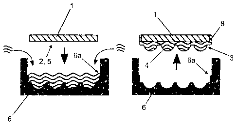
Firstly, an open casting mould 6 (see Fig. 2) is provided that contains the
negative moulds of the
formations for the optical elements 4. Moreover, supports 6a in the form of
fins or lugs support-
ing the substrate 1 in a certain position are provided in the mould 6.
Then, the surface 5 of the substrate 1 to be coated is coated with an adhesion
promoter 2, pos-
sibly after a cleaning step. The coating then proceeds, for example, by
applying droplets of the
substance and blowing-off any excess of the substance, which also dries the
remaining adhe-
sion promoter. In the ideal case, the thickness of the adhesion promoter
applied is equal to just
one monolayer, in any case it is preferred to be less than 100 nm.
As soon as the substrate is prepared as described, a silicone mixture of two
components is pro-
duced and placed in the open casting mould. One of said components contains a
catalyst and
the other component contains a cross-linker. The mixture has a viscosity of
less than 50 mPa*s
in the present case. As a matter of principle, mixing the components initiates
the curing process
though this process proceeds quite slowly at low temperatures such as room
temperature.
CA 02865225 2014-08-21
9
Subsequently, the substrate is placed in the casting mould in controlled
manner with the coated
surface 5 facing downwards and immersed into the silicone mixture (see left
side of Fig. 2).
In particular, an overflow 7 can be provided on the casting mould in this
context, as shown
schematically in Fig. 3. The overflow and the low viscosity of the silicone
jointly ensure that the
depth of immersion of the substrate is well-defined and, in particular, that
any silicone displaced
by the substrate can flow off. By this means, it can be ensured in any case of
need that not only
the surface 5 of the substrate, but also the front sides of the substrate get
covered by a circum-
ferential rim 8 of layer 3, whereas a back side 9 of the substrate is not
being coated. Complete
enveloping of the substrate may be desirable in other embodiments, though.
The rim 8 has not only a protective function for the carrier substrate 1, if
same is supported on
its rim or upon a number of said modules being arranged edge to edge, but it
also enables di-
rect, gap-less, transparent arrangement of the substrates and thus
minimisation of the deviation
of light at the optical boundaries between two carrier substrates.
Once the substrate is positioned on the supports 6a, it is checked according
to need whether
the surface 5 is wetted completely and, in particular, without forming
bubbles. In a possible re-
finement of the invention, the immersion of the substrate can just as well
proceed in a vacuum
in order to prevent the air bubble issue. However, due to the viscosity being
low, bubble-free
coating can generally be attained in the absence of a vacuum as well.
After the positioning, the silicone is cured and/or cross-linked. This is
accelerated significantly in
expedient manner through increasing the temperature. Typically, curing can be
completed in
half an hour at a temperature of approx. 100 C. At temperatures in the range
of 150 C, curing
can typically be completed in just a few minutes. The selection of the
temperature for this ther-
mal curing process must take also into consideration the properties of the
respective substrate.
Once the silicone is cured, the substrate, now coated, can be taken out of the
re-usable casting
mould as shown on the right side in Fig. 2.
CA 02865225 2014-08-21
Since highly pure silicone without any admixture of adhesion promoter in the
silicone is used in
the present case, no further measures aimed at releasing the silicone 3 from
the mould 6 are
required. In particular, the casting mould is not being lined with a release
film or the like. This
simplifies the production and enables very exact reproduction of the
structures of the casting
5 mould.
The method described above can be applied repeatedly to the same object, if
required. Fig. 5
and Fig. 6 show embodiments of the invention, which each show such refinements
of examples
from Fig. 4. In each case, after producing a first layer 3 having optical
elements 4, a second
10 layer 3' having optical elements 4' was produced.
In the case of the example according to Fig. 5, the second layer 3' was
applied onto the back
side and/or opposite sides of the substrate 1 which is provided as a planar
plate in the present
case. For this purpose, the substrate simply needs to be provided with an
adhesion promoter 2
on the yet uncoated side 9 and then inserted forward in a corresponding
casting mould 6. The
further procedural steps correspond to the procedure described above.
In the example shown in Fig. 5, the first surface 5, which is the front side
of the substrate 1, has
been coated with a plurality of collecting lenses 4 for purposes of
illustration. The second sur-
face 9, which is the back side of the substrate 1, has been coated with
Fresnel lenses 4' which
each are aligned with the collecting lenses 4.
In the example shown in Fig. 6, firstly, a layer 3 having Fresnel lenses in
the present case, was
applied to the first surface 5, which is the front side of the substrate.
Subsequently, an adhesion
promoter 2 was applied onto said layer 3 and a second layer 3' having
collecting lenses 4' was
then applied onto the first layer 3. In this case, the first layer 3 applied
is the substrate according
to the scope of the invention and its external surface is the second surface
9.
As a matter of principle, the number and design of such multiple layers are
not limited in any
way.
The layers can just as well differ in composition of the casting material, in
particular be different
casting materials and/or admixtures to the casting materials. Accordingly,
different properties
CA 02865225 2014-08-21
11
can be thus combined or the optical properties obtained by application of many
layers can be
influenced nearly gradually, e.g. by means of slightly changing the refractive
index of the casting
material used. Likewise, the final current boundary layer can be influenced
and changed before
applying the next layer, e.g. through
silanising a silicone boundary layer, dielectric or metallic coating by means
of sputtering, spray-
ing, wetting or any other customary surface coating procedures.
The use of particularly pure silicone is specified above as being preferred in
order to optimise
high degrees of transmission and material resistance in critical wavelength
ranges. As a matter
of principle, the casting material can be filled with optically effective
materials in order to thus
generate further optical functionalities, such as, e.g., conversion of the
wavelength of light by
means of introducing phosphorescent and fluorescent substances, such as, e.g.
rare earth ele-
ments, or for affecting the opacity of the optical system by means of
introducing scattering sub-
stances, such as, e.g., transparent or translucent particles (e.g. made of
glass or ceramic mate-
rials) or metallic particles.
Fig. 7 shows a preferred use of an optical system 10, as described above, in
combination with a
two-dimensional light source. The light source is provided in this case as LED
module 11 having
a number of LEDs arranged in an array. The optical system is situated at a
distance in front of
the light source and refracts the light of the individual LEDs in desired
manner, by means of
collecting lenses that are each assigned to one LED.
Fig. 8 shows another preferred use, in which a module according to the
invention according to
Fig. 1 is combined with a module according to the invention according to Fig.
4. Overall, a first
optical module is present that is provided as LED module 1, 1a, lb having a
primary optical sys-
tem 3. A second optical module provided as optical system 10 is arranged
upstream of the first
optical module. Preferably, both modules comprise multiple collecting lenses,
each correlated to
the LEDs, which act in concert to transport a large opening angle of the LEDs.