Note : Les descriptions sont présentées dans la langue officielle dans laquelle elles ont été soumises.
CA 02869294 2014-10-01
1
DESCRIPTION
Title of Invention
MAGNETIC SENSOR
Technical Field
[0001] The present disclosure relates to a magnetic sensor that detects
a small
magnetic pattern formed on a sheet-like medium such as paper currency.
Background Art
[0002] A magnetic sensor is a sensor that uses a magnetoresistance
element having
a property in which the resistance varies according to magnetic field
strength. The
magnetization of a magnetic pattern included in a sheet-like medium such as
paper
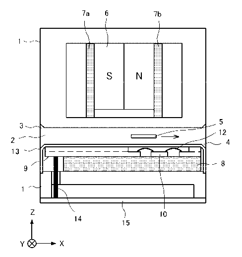
currency is typically small. For this reason, particularly in a line-type
magnetic sensor
that detects multiple channels simultaneously, an anisotropic
magnetoresistance element
is often used in order to detect a magnetic pattern with high sensitivity. An
anisotropic
magnetoresistance element generally is more sensitive than a semiconductor
magnetoresistance element. In a magnetic sensor, it is necessary to provide
anisotropic
magnetoresistance elements in areas of magnetic field strength where the
sensitivity rises
without any reaching magnetic saturation, and then convey a sheet-like medium
such as
paper currency through the strong magnetic field range.
[0003] However, in a magnetic sensor using an anisotropic magnetoresistance
element, since an anisotropic magnetoresistance element saturates at a
magnetic flux
density of approximately 10 mT, it is difficult to dispose multiple
anisotropic
magnetoresistance elements in areas of magnetic field strength where the
sensitivity rises
without saturating.
[0004] In order to solve such a problem, Patent Literature I discloses a
magnetic
sensor in which a permanent magnet is disposed with the position adjusted so
that the
bias magnetic field strength in the magneto-sensing direction of ferromagnetic
thin film
CA 02869294 2014-10-01
2
magnetoresistance elements (anisotropic magnetoresistance elements)
simultaneously
imparted by a detecting magnetic field from the permanent magnet reaches a
magnetic
flux that is not greater than the saturation magnetic field.
[0005] The magnetic sensor in Patent Literature 1 disposes a
magnetoresistance
element between a magnet and the object of detection. Besides the above, there
are
magnetic sensors configured so that the object of detection is moved between a
magnet
and a magnetoresistance element (see Patent Literature 2, for example), or,
configured so
that a magnetoresistance element is disposed between two magnets, and the
object of
detection is moved between the magnetoresistance element and one of the
magnets (see
Patent Literature 3, for example). With the configuration that moves the
object of
detection between a magnet and a magnetoresistance element, sometimes a magnet
and a
magnetized body are disposed opposite each other, and a magnetoresistance
element is
disposed on the side of the magnetized body.
[0006] For example, in the magnetic sensor in Patent Literature 4, a
permanent
magnet and a magnetized yoke are disposed opposite each other with a travel
space
therebetween, with the permanent magnet disposed below and the magnetized yoke
disposed above. The opposing magnetic pole face of the permanent magnet forms
the
same magnetic polarity. A magnetoresistance element constituting a voltage-
dividing
circuit is installed on the side of the opposing face of the magnetized yoke.
A groove is
formed in the opposing face of the magnetized yoke. Lines of magnetic force
coming
from the permanent magnet converge and enter the magnetic pole of the
magnetized yoke,
and by disposing the magnetoresistance element in this magnetic flux
convergence area,
the resolution at which an object may be detected is raised.
[0007] Also, in the magnetic sensor of Patent Literature 5, the
magnetized yoke is
disposed above the magnet. A magnetic leg portion of the magnetized yoke has
shape
magnetic anisotropy, which suppresses the spread of the magnetic flux of the
magnet.
Citation List
CA 02869294 2014-10-01
3
Patent Literature
[0008] Patent Literature 1: Unexamined Japanese Patent Application
Kokai
Publication No. 2008-145379
Patent Literature 2: Unexamined Japanese Patent Application Kokai Publication
No. 2005-129009
Patent Literature 3: Unexamined Japanese Patent Application Kokai Publication
No. 2001-21631
Patent Literature 4: Unexamined Japanese Patent Application Kokai Publication
No. H06-231336
Patent Literature 5: Unexamined Japanese Patent Application Kokai Publication
No. H07-210833
Summary of Invention
Technical Problem
[0009] The magnetic sensor described in Patent Literature 1 does not
disclose a
specific method of disposing the permanent magnet so that the bias magnetic
field
strength in the magneto-sensing direction of ferromagnetic thin film
magnetoresistance
elements reaches a magnetic flux that is not greater than the saturation
magnetic field.
In addition, although it is necessary to make a uniform bias magnetic field
strength in the
magneto-sensing direction applied to multiple ferromagnetic thin film
magnetoresistance
elements in order to output on multiple channels, the method thereof is not
disclosed.
[0010] In order to improve sensitivity of detecting an object of
detection in a
contactless magnetic sensor, it is necessary to increase the magnetic strength
of the bias
magnet, and increase the magnetic field strength of the conveyance path along
which the
object of detection is conveyed while applying an appropriate bias magnetic
field to an
anisotropic magnetoresistance element. In the magnetic sensor of Patent
Literature 1,
since the object of detection passes farther away from the bias magnet than
the
anisotropic magnetoresistance element, the variation in the magnetic field
strength due to
CA 02869294 2014-10-01
4
the object of detection is small, and the output signals from the individual
anisotropic
magnetoresistance elements are small.
[0011] In the magnetic sensors of Patent Literature 2 to 5, there is
large spatial
variation in the magnetic field strength near the areas where the
magnetoresistance
elements are disposed. The magnetoresistance elements are disposed in an area
of large
variation in magnetic field strength in the magneto-sensing direction, and
there is a
narrow range in which an optimal bias magnetic field may be obtained, making
adjustment difficult.
[0012] The present disclosure has been devised in light of
circumstances such as the
above, and takes as an object to detect the magnetic pattern of an object of
detection
consistently and with good sensitivity in a contactless state in which the
object of
detection having the magnetic pattern is separated from a magnetoresistance
element by a
minute distance.
Solution to Problem
[0013] In order to achieve the above object, a magnetic sensor according to
the
present disclosure is provided with a magnet, disposed on one face of a
conveyance path
of an object of detection, that includes a magnetic pole of designated length
along the
conveyance direction of the object of detection, and a magnetic body, disposed
opposite
the magnet along the conveyance direction with the conveyance path
therebetween.
The magnetic body generates a cross magnetic field that crosses the conveyance
path
formed between the magnetic body and the magnet. Also provided is a
magnetoresistance element, disposed on the side of the magnetic body facing
the
conveyance path, and having magneto-sensing action in the conveyance
direction.
Advantageous Effects of Invention
[0014] According to the present disclosure, fluctuations in the bias
magnetic field
strength in the magneto-sensing direction applied to an anisotropic
magnetoresistance
element are decreased, enabling the magnetic pattern of an object of detection
to be
CA 02869294 2014-10-01
detected consistently and with good sensitivity.
Brief Description of Drawings
[0015] FIG. 1 is a planar cross-section view in the conveyance direction
of an
object of detection in a magnetic sensor according to Embodiment 1 of the
present
5 disclosure;
FIG. 2 is a cross-section view when viewing the magnetic sensor according to
Embodiment 1 from the insertion/ejection direction of an object of detection;
FIG. 3 is an enlarged view illustrating the mounted state of a substrate and
an
AMR element on a magnetic carrier in FIG. 1;
FIG. 4 is a top view illustrating the mounted state of an AMR element when
viewing the substrate side from the hollow section in FIG. 1;
FIG. 5 is a connection diagram illustrating the connected state between an AMR
element of the magnetic sensor according to Embodiment 1, and an external
circuit;
FIG. 6 is a diagram illustrating a magnetic figuregenerated from a magnet,
yokes,
and magnetic carrier in the magnetic sensor according to Embodiment 1;
FIG. 7A is a magnetic line of force vector diagram explaining the detection
principle of the magnetic sensor according to Embodiment 1;
FIG. 7B is a magnetic line of force vector diagram when an object of detection
approaches an AMR element;
FIG. 7C is a magnetic line of force vector diagram when an object of detection
moves away from an AMR element;
FIG. 8 is a diagram illustrating explaining a numerically calculated
configuration
in order to explain the detection principle of the magnetic sensor according
to
Embodiment 1;
FIG. 9 is a diagram illustrating a distribution in the conveyance direction of
the
conveyance direction component of the magnetic flux density in the
configuration of FIG.
8;
CA 02869294 2014-10-01
6
FIG. 10 is a diagram illustrating a distribution in the conveyance direction
of the
spacing direction component of the magnetic flux density in the configuration
of FIG. 8;
FIG. 11 is a diagram illustrating an example of the applied magnetic flux
density
and resistance variation ratio of an AMR element;
FIG. 12 is a top view of an AMR element having a meandering resistance
pattern;
FIG. 13 is a top view illustrating the mounted state in the case modifying the
magnetic resistance pattern to a T-shaped configuration;
FIG. 14 is a top view of the AMR element having a meandering resistance
pattern
in FIG. 13;
FIG. 15 is a planar cross-section view in the conveyance direction of an
object of
detection in a magnetic sensor according to Embodiment 2 of the present
disclosure;
FIG. 16 is a planar cross-section view in the conveyance direction of an
object of
detection in a magnetic sensor according to Embodiment 3 of the present
disclosure;
FIG. 17 is a cross-section view of the magnetic sensor according to Embodiment
3
as viewed from the insertion/ejection direction of an object of detection;
FIG. 18 is a diagram illustrating the arrangement of components constituting a
magnetic circuit in the magnetic sensor according to Embodiment 3;
FIG. 19 is a diagram illustrating a magnetic figure in the configuration of
FIG. 18;
FIG. 20 is a diagram illustrating the relationship between the magnetic flux
density
applied to a magnetoresistance element and the resistance of the
magnetoresistance
element;
FIG. 21 is a diagram illustrating a distribution in the conveyance direction
of the
conveyance direction component of the magnetic flux density in the
configuration of FIG.
18;
FIG. 22 is a diagram illustrating the arrangement of components constituting a
magnetic circuit according to Embodiment 4 of the present disclosure;
FIG. 23 is a diagram illustrating a magnetic figure in the configuration of
FIG. 22;
CA 02869294 2014-10-01
7
and
FIG. 24 is a diagram illustrating a distribution in the conveyance direction
of the
conveyance direction component of the magnetic flux density in the
configuration of FIG.
22.
Description of Embodiments
[0016] Hereinafter, embodiments of the present invention will be
described with
reference to the drawings. Note that in the drawings, the same signs are given
to the
same or corresponding parts.
[0017] Embodiment 1.
FIG. 1 is a planar cross-section view in the conveyance direction of an object
of
detection in a magnetic sensor according to Embodiment 1 of the present
disclosure.
FIG. 2 is a cross-section view when viewing the magnetic sensor according to
Embodiment 1 from the insertion/ejection direction of an object of detection.
A hollow
section 2 is formed inside a housing 1. A first slit section 3 is formed along
the
scanning width (the direction orthogonal to the conveyance direction of the
object of
detection) in one of the side faces (side walls) of the housing 1, and a
second slit section 4
is formed parallel to the first slit section 3 in the other side face (side
wall). The first slit
section 3 and the second slit section 4 are connected via the hollow section
2. For
example, an object of detection 5 containing a magnetic pattern to be detected
is inserted
from the first slit section 3, conveyed using the hollow section 2 as a
conveyance path,
and ejected from the second slit section 4.
[0018] A magnet 6 having an S pole and an N pole along the conveyance
direction
is disposed on one face in the conveyance direction in the hollow section 2,
and is
distanced from the object of detection 5 in the housing 1. A magnetic carrier
8 is
disposed on the other face opposing the magnet 6 in the hollow section 2, and
is distanced
from the object of detection 5 in the housing 1. The magnetic carrier 8 is a
soft
magnetic body such as iron. Magnet yokes 7a and 7b, which make a pair for
improving
CA 02869294 2014-10-01
8
magnetic field uniformity, are disposed on both side faces of the magnet 6 in
the
conveyance direction. Assume that the conveyance direction of the object of
detection 5
(for example, paper currency) is the X-axis direction, the scanning width
direction of the
conveyance path is the Y-axis direction, and the direction in which the magnet
6 and the
magnetic carrier 8 oppose each other is the Z-axis direction.
[0019] An anisotropic magnetoresistance element (hereinafter designated
an AMR
element) 10 is disposed on the conveyance path side of the magnetic carrier 8,
and is
distanced from the object of detection 5. A substrate 9 surrounding the AMR
element
and formed with a resin such as glass epoxy is placed on the magnetic carrier
8. The
10 AMR element 10 is equipped with a resistor on a substrate surface such
as silicon or glass,
and has a property by which the resistance changes according to changes in the
magnetic
field orthogonal to the direction of current flowing in this resistor. The AMR
element
10 is disposed so as to have magneto-sensing action in the conveyance
direction of the
object of detection 5.
[0020] The conveyance path side of the substrate 9 and the AMR element 10
is
covered by an electric shield plate 13. The electric shield plate 13 transmits
magnetic
lines of force without being magnetized itself. A processing circuit 15 is
disposed
underneath the housing 1. The substrate 9 and the processing circuit 15 are
connected
by a cable 14.
[0021] FIG. 3 is an enlarged view illustrating the mounted state of the
substrate and
the AMR element on the magnetic carrier in FIG. 1. FIG. 4 is a top view
illustrating the
mounted state of the AMR element when viewing the substrate side from the
hollow
section in FIG. 1. In FIGS. 3 and 4, the substrate 9 is affixed to the
magnetic carrier 8.
The substrate 9 includes a hole section 9a, and in the case of a large circuit
scale, may
also be configured as a multilayer substrate.
[0022] The AMR element 10 is affixed by an adhesive to the surface of
the
magnetic carrier 8 exposed by the hole section 9a, so as to be surrounded by
the substrate
CA 02869294 2014-10-01
9
9. Electrodes 101a, 101b, and 101c of the AMR element 10 are respectively
connected
to electrodes 111a, 111b, and 111c provided on the substrate 9 by metal wires
12. The
electrodes 111a, 111b, and 111c are respectively connected to external pads
112a, 112b,
and 112c provided on a back face external to the substrate 9 via transmission
lines 11.
The external pads 112a, 112b, and 112c are connected to external circuits such
as an
amplifier circuit, a signal processing circuit, and a bias voltage. Note that
the hole
section 9a of the substrate may also be encapsulated with a resin or the like
in order to
protect the AMR element 10 and the metal wires 12.
[0023] In FIG. 4, resistor patterns 102a and 102b of the AMR element 10
are
disposed in parallel so that the long edges of rectangular shapes extend in
the scanning
width direction (Y-axis direction). The adjacent resistor patterns 102a and
102b are
connected in series, and this series connection is connected to the electrode
101b of the
AMR element 10, while the other end of the resistor pattern 102a is connected
to the
electrode 101a, and the other end of the resistor pattern 102b is connected to
the electrode
101c.
[0024] FIG. 5 is a connection diagram illustrating the connected state
between an
AMR element of a magnetic sensor according to Embodiment 1, and an external
circuit.
The electrode 101a is connected to the electrode 111a by a metal wire 12
(electrical
connecting means), and is connected to a DC power source voltage Vcc via the
external
pad 112a. The electrode 101b is connected to the electrode I I lb by a metal
wire 12,
and is connected to a processing circuit 15 that processes a signal via the
external pad
112b. The electrode 101c is connected to the electrode 111c by a metal wire
12, and is
connected to DC ground (GND) via the external pad 112c.
[0025] FIG. 6 is a diagram illustrating a magnetic figure generated from
a magnet,
yokes, and magnetic carrier in the magnetic sensor according to Embodiment 1.
Note
that FIG. 6 depicts the structural elements from FIG. 1 that are relevant to
explaining the
magnetic figure, and omits other structural elements.
CA 02869294 2014-10-01
[0026] As illustrated in FIG. 6, because of the property of lines of
magnetic force to
be incident perpendicular to the magnetic pole face of a magnetic body (the Bz
direction),
near the surface of the magnetic carrier 8, the magnetic flux density
component in the
X-axis direction (Bx) is extremely small, and the magnetic flux density
component (Bz)
5 in the spacing direction (Z-axis direction) forms the primary component.
The AMR
element 10 is provided on the surface of the magnetic carrier 8, where Bx is
extremely
small while the magnetic flux density component (Bz) in the spacing direction
(Z-axis
direction) has a high magnetic field strength. The object of detection 5
passes through a
position where the magnetic flux density (Bz) in the spacing direction has a
high
10 magnetic field strength, so as to cross the magnetic field in the
spacing direction.
[0027] Preferably, the center of the AMR element 10 in the conveyance
direction is
offset forwards or backwards in the conveyance direction from the center of
the magnet 6
in the conveyance direction. In addition, the center of the AMR element 10 in
the
conveyance direction is preferably disposed farther outward from the magnet 6
than the
junction face between the magnet 6 and the yoke 7b. Also, the edge of the
magnetic
carrier 8 on the side where the AMR element 10 is disposed (the yoke 7b side)
in the
conveyance direction on the face opposing the magnet 6 and closest to the
magnet 6
preferably extends past the range of the magnet 6 from the edge of the magnet
6 in the
conveyance direction on the same side. Note that the edge on the side of the
magnetic
carrier 8 opposite to where the AMR element 10 is disposed (the yoke 7a side)
may be
within the range of the magnet 6.
[0028] In FIG. 6, near where the resistor patterns 102a and 102b of the
anisotropic
magnetoresistance element (AMR element) 10, the primary component of the line
of
magnetic force is a component that proceeds from the N pole of the magnet 6 to
the
magnetic carrier 8, and acts as a cross magnetic field crossing the conveyance
path.
Above the resistor patterns 102a and 102b, a line of magnetic force 20 is
slightly tilted in
the conveyance direction (X-axis direction) from the spacing direction (Z-axis
direction),
CA 02869294 2014-10-01
11
as illustrated in FIG. 7A. For this reason, the conveyance direction (X-axis
direction)
component of this magnetic field acts as a bias magnetic field on the AMR
element 10.
[0029] As illustrated in FIG. 7B, as the object of detection (paper
currency) 5
including a magnetic pattern approaches the AMR element 10, the line of
magnetic force
20 tilts towards the magnetic pattern, and thus the magnetic flux density (Bx)
in the
conveyance direction (X-axis direction) becomes smaller. As illustrated in
FIG. 7C, as
the object of detection (paper currency) 5 (magnetic pattern) moves away from
the AMR
element 10, the line of magnetic force 20 tilts towards the magnetic pattern,
and thus the
magnetic flux density (Bx) in the conveyance direction (X-axis direction)
becomes larger.
For this reason, the resistance of the AMR element 10 that magnetically senses
the
X-direction component changes, enabling sensing of the magnetic pattern.
[0030] FIG. 8 is a diagram illustrating explaining a numerically
calculated
configuration in order to explain the detection principle of the magnetic
sensor according
to Embodiment I. Note that FIG. 8 depicts the structural elements from FIG. 1
that are
relevant to explaining the magnetic figure, and omits other portions.
[0031] FIG. 9 is a diagram illustrating a distribution in the conveyance
direction of
the conveyance direction component of the magnetic flux density in the
configuration of
FIG. 8. The configuration of FIG. 8 illustrates the result of using a
neodymium sintered
magnet for the material of the magnet 6, and calculating the change in
strength of the
magnetic flux density in the X-axis direction (Bx) over the conveyance
direction of the
object of detection 5 (X-axis direction). In FIG. 9, the spacing direction (Z-
axis
direction) between the opposing magnet 6 and magnetic carrier 8 is varied
between Z =
0.1 mm to 0.6 mm as a parameter. Note that the origin of the X-axis direction
is taken
to be the center of the magnet 6, and the origin of the Z-axis direction is
taken to be the
surface of the magnetic carrier 8.
[0032] FIG. 10 is a diagram illustrating a distribution in the
conveyance direction of
the spacing direction component of the magnetic flux density in the
configuration of FIG.
CA 02869294 2014-10-01
12
8. The configuration of FIG. 8 illustrates the result of calculating the
change in strength
of the magnetic flux density in the Z-axis direction (Bz) over the conveyance
direction of
the object of detection 5 (X-axis direction). In FIG. 10, the spacing
direction (Z-axis
direction) between the opposing magnet 6 and magnetic carrier 8 is varied
between Z
0.5 mm to 2 mm as a parameter. Note that the origin of the X-axis direction is
taken to
be the center of the magnet 6, and the origin of the Z-axis direction is taken
to be the
surface of the magnetic carrier 8.
[0033] FIG. 11 is a diagram illustrating an example of the applied
magnetic flux
density and resistance variation ratio of an AMR element. In the case of using
the AMR
element 10 with a saturation magnetic flux density of 10 mT illustrated in
FIG. 11 as the
AMR element 10, a suitable sensitivity is obtained around a Bx of -2 to -6 mT
(bias
magnetic field range A) and around +2 to 6 mT (bias magnetic field B). For
this reason,
it is necessary to dispose the AMR element 10 so that each Bx applied to the
resistor
patterns 102a and 102b of the AMR element 10 is contained within the above
bias
magnetic field range A or bias magnetic field range B.
[0034] According to FIG. 9, in the case in which the thickness of the
AMR element
10 is 0.3 mm (Z = 0.3 mm), for example, it is sufficient to dispose the AMR
element 10
at a position of X = 3.7 mm to 4.8 mm in order for the Bx applied to the
resistor patterns
102a and 102b to be contained in the bias magnetic field range A. It is
possible to put
the AMR element 10 in a bias magnetic field range with a very loose assembly
precision
of Al mm or more. Particularly, in a line sensor in which multiple AMR
elements 10
are disposed in the scanning width direction, fluctuations in bias magnetic
field strength
in the magneto-sensing direction of the respective AMR elements 10 are
decreased, and
the configuration is extremely effective at minimizing fluctuations across
channels.
Note that this advantageous effect enables looser assembly precision for not
only the
AMR element 10, but also the magnet 6 and the magnetic carrier 8.
[0035] In addition, change in the magnetic field when the object of
detection 5
CA 02869294 2014-10-01
13
(magnetic pattern) is exerted on the resistor patterns 102a and 102b is
proportional to the
magnetic field near the object of detection 5 (the magnetic field applied to
the object of
detection 5). When detecting this change in the magnetic field with the AMR
element
10, it is necessary to apply a larger magnetic field to the object of
detection 5 in order to
achieve higher output. In Embodiment 1, the magnetic flux density applied to
the object
of detection 5 is Bz = approx. 180 mT according to FIG. 10, and the magnetic
pattern of
the object of detection 5 is detected with good sensitivity even if the AMR
element 10
and the object of detection 5 are separated.
[0036] According to the configuration of Embodiment 1, even if the
magnetic
strength of the magnet 6 is increased to achieve higher output, the Bx applied
to the
resistor patterns 102a and 102b of the AMR element 10 is small. For this
reason, it is
possible to obtain consistent output in a magnetic sensor without greatly
worsening the
assembly precision.
[0037] In addition, if the thickness of the AMR element 10 is made
thinner, the Bx
applied to the resistor patterns 102a and 102b becomes smaller, thus enabling
stable
usage of the AMR element 10 with higher sensitivity (that is, the slope in
FIG. 11
becomes steeper), and making it possible to raise the sensitivity of the AMR
element 10
in order to raise output.
[0038] Similarly, even in the case of using the bias magnetic field
range B, in FIG.
9, if the thickness of the AMR element 10 is 0.3 mm (Z = 0.3 mm), for example,
it is
sufficient to dispose the AMR element 10 at a position X = 6.2 mm to 9.8 mm.
At this
point, the magnetic flux density applied to the object of detection 5 is Bz =
approx. 130
mT to 170 mT according to FIG. 10. Compared to the bias magnetic field range
A, the
output lowers somewhat when the AMR element 10 and the object of detection 5
are
separated, it is possible to detect the magnetic pattern of the object of
detection 5 with
good sensitivity and an extremely loose assembly precision of A3 mm or more.
[0039] In this way, since a strong magnetic field in the spacing
direction (Z-axis
CA 02869294 2014-10-01
14
direction) is applied to the object of detection 5, even if the AMR element 10
and the
object of detection 5 are separated, the magnetic pattern of the object of
detection 5 is
detected with good sensitivity. In addition, since the bias magnetic field
strength in the
conveyance direction (X-axis direction) applied to the resistor patterns 102a
and 102b of
the AMR element 10 varies slightly across positions in the X-axis direction,
the assembly
tolerance for a fixed sensitivity requirement broadens, and inconsistencies in
sensitivity
are reduced. Furthermore, by making the thickness of the AMR element 10
thinner, the
magnetic strength of the magnet 6 may be increased in order to improve output.
Also,
consistent output over multiple channels is obtained, even if the sensitivity
of the AMR
element 10 is raised. Furthermore, since the magnet 6 and the magnetic carrier
8 are
disposed opposite each other, a stable magnetic path is formed, and the
magnetic pattern
of the object of detection 5 is consistently detected while being resistant to
the effects of
external magnetic bodies.
[0040] FIG. 12 is a top view of an AMR element having a meandering
resistance
pattern. In FIG. 4, the resistor patterns 102a and 102b of the AMR element 10
are
rectangular shapes, but as illustrated in FIG. 12, may also be meandering
shapes disposed
so that the long edges extend in the scanning width direction (Y-axis
direction). In this
case, the resistance values of the resistor patterns 102a and 102b increase
and become
higher resistance values than those of the rectangular shapes, thereby
improving the
sensitivity of the AMR element 10 for detecting change in the magnetic field,
and
increasing the detection sensitivity of the magnetic sensor.
[0041] FIG. 13 is a top view illustrating the mounted state in the case
modifying the
magnetic resistance pattern to a T-shaped configuration. The arrangement of
the resistor
patterns 102a and 102b of the AMR element 10 may also be a vertical
arrangement as
illustrated in FIG. 13. Also, even in the case of this arrangement, the
resistor patterns
102a and 102b may have a meandering shape as illustrated in FIG. 14.
[0042] In Embodiment 1, the magnet 6 is configured to have a pair of
yokes 7a and
CA 02869294 2014-10-01
7b disposed in order to improve the magnetic field uniformity at either side
face in the
conveyance direction, but the yokes 7a and 7b may also be omitted.
[0043] Additionally, although the magnet 6 is disposed in an S pole, N
pole order
from the first slit section 3 along the conveyance direction of the object of
detection 5, the
5 magnet 6 may also be disposed as N pole, S pole.
[0044] Note that in Embodiment 1, although an AMR element 10 is used as
a
magnetoresistance element, a giant magnetoresistance (GMR) element or a
tunneling
magnetoresistance (TMR) element may also be used.
[0045] Embodiment 2.
10 FIG. 15 is a
planar cross-section view in the conveyance direction of an object of
detection in a magnetic sensor according to Embodiment 2 of the present
disclosure.
Embodiment 1 describes a configuration in which the magnet 6 is disposed
having S pole,
N pole along the conveyance direction of the object of detection 5. In
Embodiment 2,
one of the magnetic poles along the conveyance direction (in FIG. 15, the N
pole) is
15 disposed on the conveyance path side.
[0046] Even with the arrangement of the magnet 6 in FIG. 15, a magnetic
field is
formed in the Z direction between the magnet 6 and the magnetic carrier, and
thus
operational advantages similar to Embodiment 1 of the present disclosure are
obtained.
[0047] Embodiment 3.
FIG. 16 is a planar cross-section view in the conveyance direction of an
object of
detection in a magnetic sensor according to Embodiment 3 of the present
disclosure.
FIG. 17 is a cross-section view of the magnetic sensor according to Embodiment
3 as
viewed from the insertion/ejection direction of an object of detection. A
hollow section
2 is formed inside the housing I. A first slit section 3 is formed along the
scanning
width (the direction orthogonal to the conveyance direction of the object of
detection) in
one of the side faces (side walls) of the housing 1, and a second slit section
4 is formed
parallel to the first slit section 3 in the other side face (side wall). The
first slit section 3
CA 02869294 2014-10-01
16
and the second slit section 4 are connected via the hollow section 2. For
example, an
object of detection 5 containing a magnetic pattern to be detected is inserted
from the first
slit section 3, conveyed using the hollow section 2 as a conveyance path, and
ejected
from the second slit section 4.
[0048] A magnet 6 having an S pole and an N pole along the conveyance
direction
is installed on one face in the conveyance direction in the hollow section 2,
and is
distanced from the object of detection 5 in the housing 1. A magnetic carrier
8 is
installed on the other face opposing the magnet 6 in the hollow section 2, and
is distanced
from the object of detection 5 in the housing 1. The magnetic carrier 8 is a
soft
magnetic body such as iron. Yokes 7a and 7b, which make a pair for improving
magnetic field uniformity, are installed on both side faces of the magnet 6 in
the
conveyance direction. The magnetic carrier 8 extends farther outward than the
yokes 7a
and 7b along the conveyance direction.
[0049] A non-magnetic carrier 16 is provided on the surface of the
magnetic carrier
8 on the conveyance path side, separated from the object of detection 5. An
anisotropic
magnetoresistance element (hereinafter designated an AMR element) 10 is
disposed on
the non-magnetic carrier 16. A substrate 9 surrounding the AMR element 10 and
formed with a resin such as glass epoxy is placed on the non-magnetic carrier
16. The
AMR element 10 is equipped with a resistor on a substrate surface such as
silicon or glass,
and has a property by which the resistance changes according to changes in the
magnetic
field orthogonal to the direction of current flowing in this resistor.
[0050] The conveyance path side of the magnet 6 and yokes 7a and 7b, as
well as
the conveyance path side of the substrate 9 and the AMR element 10, are
respectively
covered by an electric shield plate 13. The electric shield plate 13 transmits
magnetic
lines of force without being magnetized itself. A processing circuit 15 is
disposed
underneath the housing 1. The substrate 9 and the processing circuit 15 are
connected
by a cable 14.
CA 02869294 2014-10-01
17
[0051] FIG. 18 is a diagram illustrating the arrangement of components
constituting
a magnetic circuit in the magnetic sensor according to Embodiment 3. FIG. 18
depicts
only the structural elements that are relevant to explaining the operation in
FIG. 16, and
omits other structural elements. The AMR element 10 is separated from the
magnetic
carrier 8 by a distance equal to the thickness of the non-magnetic carrier 16.
[0052] FIG. 19 is a diagram illustrating a magnetic figure in the
configuration of
FIG. 18. Magnetic lines of force are distributed such that magnetic lines of
force from
the yokes 7a and 7b are concentrated in the magnetic carrier 8. The dashed
line 30
indicates the position of the AMR element 10 with respect to the magnetic
carrier 8.
The height from the surface of the magnetic carrier 8 to the AMR element 10 is
approximately 0.4 mm, for example. The AMR element 10 is disposed on this
dashed
line 30 at a position farther outward from the magnet 6 than the junction
between the
yoke 7a and the magnet 6.
[0053] In Embodiment 1, the AMR element 10 is disposed on the ejection
side of
the conveyance path from the center of the magnet 6 in the conveyance
direction. In
contrast, in Embodiment 3, the AMR element 10 is disposed on the insertion
side of the
conveyance path from the center of the magnet 6 in the conveyance direction.
Since the
magnet 6 is symmetrical about the center of the conveyance direction, the AMR
element
10 may be placed on either of the insertion side and the ejection side of the
conveyance
path with respect to the magnet 6.
[0054] The AMR element 10 is disposed on the dashed line 30 at a
position farther
outward from the magnet 6 than the junction between the yoke 7a and the magnet
6, and
is placed inside the magnetic field formed by the magnet 6, the yokes 7a and
7b, and the
magnetic carrier 8. For example, if a magnetic pattern formed on an object of
detection,
such as an object of detection 5 on which is applied ink that contains a
magnetic material,
passes through this magnetic field, the magnetic field distribution changes,
and the
magnetic field being applied to the anisotropic magnetoresistance element 10
changes.
CA 02869294 2014-10-01
18
Consequently, this change may be electrically sensed as a change in
resistance.
[0055] FIG. 20 is a diagram illustrating the relationship between the
magnetic flux
density applied to a magnetoresistance element and the resistance of the
magnetoresistance element. In FIG. 20, if the magnetic flux density is
increased or
decreased from a state of 0 magnetic flux density, the resistance of the AMR
element 10
changes, and the resistance becomes nearly constant when the magnetic flux
density is
equal to or greater than, or less than or equal to, certain values. This state
in which the
absolute value of the magnetic flux density becomes large and the resistance
becomes
nearly constant is called saturation. In the case in which the change in the
magnetic flux
density attempted to be measured using the magnetoresistance element is small
versus the
magnitude of the magnetic flux density reached when the magnetoresistance is
in a
saturated state, if a DC magnetic flux density with a magnitude indicated by
the chain line
40 in FIG. 20 is applied, for example, the change in resistance due to the
change in the
magnetic flux density attempted to be measured will increase, making it
possible to
obtain a large electrical signal. A magnetic field that applies DC magnetic
flux density
as indicated by the chain line 40 is called a bias magnetic field.
[0056] As the magnetic figure illustrated in FIG. 19 demonstrates, since
the lines of
magnetic force 20 are incident perpendicular to the magnetic carrier 8, for
the AMR
element 10 located at a place slightly distanced from the magnetic carrier 8,
the X-axis
direction component of the magnetic flux density (hereinafter denoted Bx)
becomes very
small. Since the Bx bias magnetic field required by the AMR element 10 is
small, a
suitable Bx bias magnetic field is obtained by placing the AMR element 10 at a
place
approximately 0.4 mm away from the magnetic carrier 8. For the bias magnetic
field to
be applied to the AMR element 10, an absolute value of approximately 2 0.5
mT is
suitable, for example.
[0057] FIG. 21 is a diagram illustrating a distribution in the
conveyance direction of
the conveyance direction component of the magnetic flux density in the
configuration of
CA 02869294 2014-10-01
19
FIG. 18. FIG. 21 is a distribution of Bx on the dashed line 30 in FIG. 19, and
is a
distribution of Bx when A= 10 mm, P= 2.3 mm, B = 19 mm, Q = 1 mm, C = 3.2 mm,
and G = 4.9 mm in FIG. 18. In FIG. 21, the horizontal axis is the distance (m)
when
treating the left edge of the magnetic carrier 8 as x = 0, while the vertical
axis is the
conveyance direction component of the magnetic flux density (T). The
distribution of
Bx is indicated by the curve 50. In FIG. 21, the range 51 indicates the
suitable bias
magnetic field of -2 0.5 mT, and the area 52 indicates the installable
position of the
AMR element 10 corresponding to this magnetic field range.
[0058] As illustrated in FIG. 21, near the location where Bx = -2 mT on
the curve
of the Bx distribution, the slope of the curve 50 is small, and the
installable range of the
AMR element 10 becomes a size of approximately 0.5 mm.
[0059] In this way, by extending the length of the magnetic carrier 8 in
the X-axis
direction outward from the yoke 7a, the slope of Bx with respect to the
conveyance
direction becomes small, which has an advantageous effect of increasing the
degree of
freedom in the installation position of the AMR element 10. Note that the
order of the
N pole and the S pole may also be the reverse of FIGS. 16 and 18.
[0060] Embodiment 4.
FIG. 22 is a diagram illustrating the arrangement of components constituting a
magnetic circuit according to Embodiment 4 of the present disclosure. The
structural
components in FIG. 22 are the same as the case of Embodiment 3, but the width
of the
magnetic carrier 8 is smaller than that of Embodiment 3. The yoke 7a side of
the
magnetic carrier 8 extends outward from the yoke 7a, but the yoke 7b side is
shortened
towards the magnet 6 side before the yoke 7h. The center 60 of the magnetic
carrier 8 in
the conveyance direction is disposed in a non-aligned state with the center 61
of the
magnet 6 in the conveyance direction.
[0061] Since the magnet 6 is symmetrical about the center of the
conveyance
direction, the AMR element 10 may be placed on either of the insertion side
and the
CA 02869294 2014-10-01
ejection side of the conveyance path with respect to the magnet 6. It is
sufficient for the
magnetic carrier 8 to extend outward past the yoke 7a or 7b along the
conveyance
direction at least on the side where the AMR element 10 is disposed.
[0062] FIG. 23 is a diagram illustrating a magnetic figure in the
configuration of
5 FIG. 22. FIG. 24 is a diagram illustrating a distribution in the
conveyance direction of
the conveyance direction component of the magnetic flux density in the
configuration of
FIG. 22. The Bx distribution at a position distanced 0.4 mm from the magnetic
carrier 8
(indicated by the dashed line 62) is plotted as shown in FIG. 24. FIG. 24 is a
Bx
distribution when C = 3.2 mm and D = 2.8 mm in FIG. 22. In FIG. 24, the
horizontal
10 axis is the distance (m) when treating the left edge of the magnetic
carrier 8 as x = 0,
while the vertical axis is the conveyance direction component of the magnetic
flux
density (T). The distribution of Bx is indicated by the curve 50. In FIG. 24,
the range
51 indicates the suitable bias magnetic field of -2 0.5 mT, and the area 52
indicates the
installable position of the AMR element 10 corresponding to this magnetic
field range.
15 [0063] FIG. 24 demonstrates that in Embodiment 4, the slope of the
magnetic flux
density with respect to conveyance direction likewise may be reduced. As a
result, the
slope of Bx with respect to the conveyance direction becomes small, which has
an
advantageous effect of increasing the degree of freedom in the installation
position of the
AMR element 10. Furthermore, the magnetic carrier 8 in use that is formed with
an iron
20 plate or the like may be made smaller, thus contributing to a more
compact configuration
and lower costs.
[0064] Various modification of the foregoing embodiments are possible
within the
scope of the spirit of the present disclosure. The foregoing embodiments are
for the
purpose of describing the present disclosure, and are not intended to limit
the scope of the
present disclosure. The scope of the present disclosure is indicated by the
attached
claims rather than the embodiments. Various modifications made within the
scope of
the claims and their equivalents are to be included in the scope of the
present disclosure.
CA 02869294 2014-10-01
21
[0065] This application claims priority based on Japanese Patent
Application No.
2012-088502 and Japanese Patent Application No. 2012-088501, filed in the
Japan
Patent Office on April 9, 2012, including specification, claims, drawings, and
abstract.
The disclosed contents ofJapanese Patent Application No. 2012-088502 and
Japanese
Patent Application No. 2012-088501 are hereby incorporated in entirety by
reference.
Reference Signs List
[0066] 1 housing
2 hollow section
3 first slit section
4 second slit section
5 object of detection (paper currency)
6 magnet
7a, 7b yoke
8 magnetic carrier
9 substrate
9a hole section of substrate
10 anisotropic magnetoresistance element (AMR element)
101a, 101b, 101c electrode of AMR element
102a, 102b, 102c resistor pattern
11 transmission line
111a, 111b, 111c electrode of transmission line
112a, 112b, 112c external pad of transmission line
12 metal wire (electrical connecting means)
13 electric shield plate
14 cable
15 processing circuit
16 non-magnetic carrier
CA 02869294 2014-10-01
22
20 line of magnetic force