Note : Les descriptions sont présentées dans la langue officielle dans laquelle elles ont été soumises.
CA 02871414 2014-10-23
=
13S0180P - 1 -
DESCRIPTION
Title of Invention
HOLOGRAM TRANSFER FOIL, FABRICATION METHOD OF IMAGE DISPLAY
ELEMENT, IMAGE DISPLAY ELEMENT, AND PERSONAL AUTHENTICATION
MEDIUM
Technical Field
Embodiments described herein relate generally to a
hologram transfer foil which is easy to identify and difficult
to counterfeit and tamper, a fabrication method of an image
display element, an image display element, and a personal
authentication medium.
Background Art
Inmost of personal identification media such as passports
or ID (identification) cards, face images are used in order that
personal authentication can be visually performed. For
example, in a general passport, printing paper on which a face
image is printed is attached to a booklet. However, there is
a concern that such a passport is tampered by re-attaching a
photoprint.
For this reason, in recent years, the information of a face
image is digitized, and the digital information is reproduced
on the booklet. As an image display technique which is used
for image reproduction, use is made of, for example, a thermal
transfer recording method by a transfer ribbon using a
sublimation (thermal migratory) dye, or a resin melting type
or wax melting type in which pigments are dispersed, or an
electrophotography technique.
CA 02871414 2014-10-23'
=
- 2 -
In recent years, printers by a thermal transfer recording
method using a sublimation dye or a colored thermoplastic resin
have been gaining in popularity. If this thermal transfer
recording method is used, it is not necessarily difficult to
remove a face image from a passport and to record another face
image on the corresponding part.
On the other hand, there has been proposed a fluorescent
printed matter on which a face image is printed by using the
above-described image display techniq-ue and a face image is
recorded thereon by using fluorescent ink (see, e.g. literature
1 (Jpn. Pat. Appin. KOKAI Publication No. 2000-141863) ) . In
addition, there have been proposed an anti-counterfeit image
formation element on which a face image is recorded by using
ink which contains a colorless or thin-color fluorescent dye
and a color pigment (e.g. literature 2 (Jpn. Pat. Appin. KOKAI
Publication No. 2002-226740) ) , and a personal authentication
medium on which an ordinary face image and a face image, which
is formed by using a pearl pigment are disposed in juxtaposition
(see, e.g. literature 3 (Jpn. Pat. Appin. KOKAI Publication
No. 2003-170685)).
By applying the above-described image display techniques
to passports, tampering of passports becomes more difficult.
However, a face image, which is recorded by using a
fluorescent material, cannot be observed unless a special light
source, such as an ultraviolet lamp, is used. In addition,
although a face image, which is formed by using a pearl pigment,
can be recognized by the naked eye, it is difficult to form an
CA 02871414 2014-10-23
=
- 3 -
image with high fineness by using the pearl pigment since the
grain size of the pearl pigment is large.
Tampering of a face is easier in a case where the look of
a face image recorded on a personal authentication medium is
simple and there is no special visual effect, than in a case
where a face image is complex and has a characteristic visual
effect. In addition, in a case where a face image is displayed
with a simple look, it is difficult to visually determine with
ease a counterfeited or tampered face image.
Summary of Invention
Technical Problem
The present invention has been made in consideration of
the above circumstance, and the object of the invention is to
provide a hologram transfer foil which is easy to identify and
difficult to counterfeit and tamper, a fabrication method of
an image display element, an image display element, and a
personal authentication medium.
Solution to Problem
A hologram transfer foil according to first embodiment is
thermally transferrable to a transfer base member. The hologram
transfer foil includes a structure configured such that a
peeling layer, a diffraction structure forming layer and an
adhesive layer are stacked on one surface of a substrate. The
diffraction structure forming layer includes fine concaves and
convexes of a hologram or a diffraction grating. At least one
of the peeling layer and the adhesive layer includes
heat-conductive hidden information in a heat-conductive hidden
CA 02871414 2014-10-23 -
=
=
- 4 -
inf ormat ion possession portion.
According to the first embodiment, the heat-conductive
hidden information maybe a geometrical pattern, a cyclically
arranged two-value character pattern, or a cyclically arranged
two-value graphic pattern. At least one of the peeling layer
and the adhesive layer may record the heat-conductive hidden
information in the heat-conductive hidden information
possession portion by forming concaves and convexes. The
heat-conductive hidden information may be recorded in the
heat-conductive hidden information possession portion by an
agglomeration state of an inclusion in the adhesive layer.
According to second embodiment, a hologram transfer foil
is thermally transferrable to a transfer base member. The
hologram transfer foil includes a structure configured such
that a peeling layer, a diffraction structure forming layer and
an adhesive layer are stacked on one surface of a substrate.
The diffraction structure forming layer includes fine concaves
and convexes of a hologram or a diffraction grating. At least
one of the peeling layer and the adhesive layer includes
heat-conductive hidden information in a heat-conductive hidden
information possession portion, and includes no hidden
information in a heat-conductive hidden information
non-possession portion.
According to the second embodiment, the diffraction
structure forming layer may be configured such that at least
one of a spatial frequency and a grating angle is different
between the heat-conductive hidden information possession
81783369
- 5 -
portion and the heat-conductive hidden information non-
possession portion.
According to third embodiment, in a fabrication method
of an image display element, the hologram transfer foil of the
second embodiment is thermally transferred to the transfer
base member. The fabrication method of an image display
element includes transferring the heat-conductive hidden
information possession portion of the hologram transfer foil
onto the transfer base member, transferring the heat-
conductive hidden information non-possession portion of the
hologram transfer foil onto the transfer base member, the
heat-conductive hidden information non-possession portion
including identification information.
According to fourth embodiment, the image display
element is fabricated by the fabrication method of the third
embodiment. The image display element includes a structure
configured such that an image receiving layer, an adhesive
layer, a diffraction structure forming layer and a peeling
layer are stacked on one surface of a substrate.
According to fifth embodiment, a personal authentication
medium comprises the image display element of the fourth
embodiment.
According to an embodiment, there is provided a hologram
transfer foil which is thermally transferrable to a transfer
base member, comprising: a structure configured such that a
peeling layer, a diffraction structure forming layer and an
adhesive layer are stacked on one surface of a substrate,
wherein the diffraction structure forming layer includes fine
CA 2871414 2018-06-15
81783369
- 5a -
concaves and convexes of a hologram or a diffraction grating,
at least one of the peeling layer and the adhesive layer
includes heat-conductive hidden information in a heat-
conductive hidden information possession portion, and includes
identification information in a heat-conductive hidden
information non-possession portion, and the diffraction
structure forming layer is configured such that at least one
of a spatial frequency and a grating angle is different
between the heat-conductive hidden information possession
portion and the heat-conductive hidden information non-
possession portion.
According to another embodiment, there is provided a
hologram transfer foil which is thermally transferrable to a
transfer base member, comprising: a structure configured such
that a peeling layer, a diffraction structure forming layer and
an adhesive layer are stacked on one surface of a substrate,
wherein the diffraction structure forming layer includes fine
concaves and convexes of a hologram or a diffraction grating,
and at least one of the peeling layer and the adhesive layer
includes heat-conductive hidden information in a heat-
conductive hidden information possession portion, and includes
no hidden information in a heat-conductive hidden information
non-possession portion, and the diffraction structure forming
layer is configured such that at least one of a spatial
frequency and a grating angle is different between the heat-
conductive hidden information possession portion and the heat-
conductive hidden information non-possession portion.
According to another embodiment, there is provided a
fabrication method of an image display element in which the hologram
CA 2871414 2018-06-15
= 81783369
- 5b -
transfer foil as described herein is thermally transferred to the
transfer base member, comprising: transferring the heat-
conductive hidden information possession portion of the
hologram transfer foil onto the transfer base member; and
transferring the heat-conductive hidden information non-possession
portion of the hologram transfer foil onto the transfer base member,
the heat-conductive hidden information non-possession portion
including identification information.
According to another embodiment, there is provided an
image display element fabricated by the fabrication method as
described herein, wherein the image display element includes a
structure configured such that an image receiving layer, an adhesive
layer, a diffraction structure foLming layer and a peeling layer are
stacked on one surface of a substrate.
According to another embodiment, there is provided a
personal authentication medium comprising the image display
element as described herein.
Advantageous Effects of Invention
According to the embodiments of the present invention,
it is possible to provide a hologram transfer foil which is
easy to identify and difficult to counterfeit and tamper, a
fabrication method of an image display element, an image
display
CA 2871414 2018-06-15
CA 02871414 2014-10-23
- 6 -
element, and a personal authentication medium.
Brief Description of Drawings
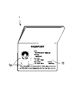
FIG. 1 is a plan view illustrating an example of a personal
authentication medium according to an embodiment.
FIG. 2 is a cross-sectional view illustrating a first
example of a hologram transfer foil according to the embodiment.
FIG. 3 is a plan view illustrating a second example of the
hologram transfer foil according to the embodiment.
FIG. 4 is a cross-sectional view illustrating the second
example of the hologram transfer foil according to the
embodiment.
FIG. 5 is a cross-sectional view illustrating the second
example of the hologram transfer foil according to the
embodiment.
FIG. 6A is a cross-sectional view illustrating an example
of a first step of a fabrication method of an image display
element according to the embodiment.
FIG. 6B is a cross-sectional view illustrating an example
of a second step of the fabrication method of the image display
element according to the embodiment.
FIG. 7 is a cross-sectional view illustrating an example
of an image display element fabricated by the fabrication method
of the image display element according to the embodiment.
FIG. 8 is a cross-sectional view illustrating an example
of a personal authentication medium on which the image display
element according to the embodiment has been transferred.
FIG. 9 is a cross-sectional view illustrating an example
CA 02871414 2014-10-23
=
- 7 -
of an observation state of the personal authentication medium
according to the embodiment.
FIG. 10A is a plan view illustrating an example of
identification information of the personal authentication
medium according to the embodiment.
FIG. 10B is a plan view illustrating an example of hidden
information of the personal authentication medium according to
the embodiment.
FIG. 11 is a schematic view illustrating an example of
comparison between a conventional image and an image according
to the embodiment.
Description of Embodiments
Embodiments relate to a hologram transfer foil, an image
display element, a fabrication method of an image display
element, and a personal authentication medium.
A hologram transfer foil according to an embodiment is
formed by stacking a peeling layer, a diffraction structure
forming layer and an adhesive layer on one surface of a
substrate. The diffraction structure forming layer is formed
of fine concaves and convexes of a hologram or a diffraction
grating. In at least one of the peeling layer and the adhesive
layer, hidden information is included in a heat-conductive
hidden information possession portion, and no hidden
information is included in a heat-conductive hidden information
non-possession portion.
An image display element according to an embodiment is
fabricated by thermally transferring a hologram transfer foil
CA 02871414 2014-10-23
- 8 -
onto a transfer base member.
A fabrication method of an image display element according
to an embodiment includes recording a heat-conductive hidden
information possession portion of a hologram transfer foil on
a transfer base member, and recording a heat-conductive hidden
information non-possession portion including identification
information of the hologram transfer foil on the transfer base
member.
According to the embodiment, it is possible to visually
confirm with ease an image for identifying a person, to prevent
counterfeiting and tampering, and to realize high security.
Next, embodiments will be described in detail with
reference to the drawings.
FIG. 1 is a plan view which schematically illustrates an
example of a personal authentication medium according to an
embodiment. A personal authentication medium 1 is, for
example, a booklet such as a passport. In FIG. 1, the personal
authentication medium 1 is depicted in an open state.
The personal authentication medium 1 displays image
information la, lb. The image information la is image
information which is displayed by making use of absorption of
light. Specifically, the image information la is an image which
is visually recognizable when the image information la is
illuminated with white light and observed by the naked eye.
The image information la may be composed of, for example,
a dye or a pigment. In this case, in the formation of the image
information la, use may be made of a thermal transfer recording
CA 02871414 2014-10-23
=
- 9 -
method using a thermal head, an ink jet recording method, an
electrophotography method, or a combination of two or more of
these methods. The image information la may be formed by
forming a layer including a thermosensitive color coupler, and
drawing an image on this layer by a laser beam. The image
information la may be formed by combining the above-described
various methods. At least a part of the image information la
may be formed by a thermal transfer recording method using a
hot stamp, may be formed by a printing method, or may be formed
by using a combination of these.
The image information lb is an image which is displayed
by a diffraction structure of a hologram and/or a diffraction
grating. For example, the image information lb is formed by
successively performing, in the named order, thermal transfer
recording using a thermal head and thermal transfer recording
using a hot stamp or a heat roll.
The image information lb includes identification
information with an intermediate gradation for authenticating
a person, and hidden information which is recognized at a visual
recognition angle which is different from a visual recognition
angle of the identification information. The identification
information with the intermediate gradation for personal
authentication is, for instance, a face image. The hidden
information is, for example, non-personal information such as
a symbol, a code and a mark.
Next, referring to FIG. 2 to FIG. 4, a description is given
of the structure of a hologram transfer foil which is necessary
CA 02871414 2014-10-23
- 10 -
for the fabrication of the personal authentication medium 1.
FIG. 2 is a cross-sectional view illustrating a first
example of the hologram transfer foil according to the
embodiment.
FIG. 3 is a plan view illustrating a second example of the
hologram transfer foil according to the embodiment.
FIG. 4 and FIG. 5 are cross-sectional views illustrating
the second second example of the hologram transfer foil
according to the embodiment.
A hologram transfer foil 100, 200 is formed by successively
stacking a peeling layer 12, 22 (22a, 22b) , a diffraction
structure forming layer 13, 23, and an adhesive layer 14, 24
(24a, 24b) on one surface of a substrate 11, 21. This hologram
transfer foil 100, 200 may be applied in the form of a hologram
ribbon or sheet.
The peeling layer 22a is a peeling layer including no
hidden information. The peeling layer 22b is a peeling layer
including hidden information.
The adhesive layer 24a is an adhesive layer including no
hidden information. The adhesive layer 24b is an adhesive layer
including hidden information.
The substrate 11, 21 is, for example, a resin film or sheet.
The substrate 11, 21 is formed by using, for example, a plastic
material such as polyethylene terephthalate (PET) ,
polyprophylene (PP) , polycarbonate (PC) ,
polymethylmethacrylate (PMMA) , or polyethylene (PE) .
The peeling layer 12, 22 is formed on the substrate 11,
CA 02871414 2014-10-23
- 11 -
21. The peeling layer 12, 22 functions to stabilize peeling
of the hologram transfer foil 100, 200 from the substrate 11,
21, and to promote adhesion to a transfer base member 301 shown
in FIG. 6 (to be described later) . The peeling layer 12, 22
has light transmissivity, and is typically transparent. As the
material of the peeling layer 12, 22, use may be made of, for
instance, a resin in which a silicone- or fluorine-based
additive is added to a thermoplastic resin such as a
polycarbonate resin, an acrylic resin, a fluorine-based acrylic
resin, a silicone-based acrylic resin, an epoxy acrylate resin,
a polystyrene resin, a cycloolef in polymer, a methylstyrene
resin, a fluorene resin, PET, polypropylene, a polyethylene
terephthalate resin or a poyacetal resin, a fluorine-based
acrylic resin, or a silicone-based acrylic resin.
The peeling layer 12, 22b is coated by, for example, a
gravure coater. In the coating by the gravure coater, by using
a plate with a pattern as a gravure printing plate, the peeling
layer 12, 22b with a finely varying thickness along the pattern
(typically, a difference in thickness is about 0.2 pm or less)
can be coated. In addition, the peeling layer 22, 22a may be
coated by a coating method of, for example, a lip coater, by
which the thickness of a coated layer becomes uniform in the
plane.
The diffraction structure forming layer 13, 23 is formed
on the peeling layer 12, 22. As the material of the diffraction
structure forming layer 13, 23, use may be made of, for example, -
a photo-curing resin such as a polycarbonate resin, an acrylic
CA 02871414 2014-10-23
=
- 12 -
resin, a fluorine-based acrylic resin, a silicone-based acrylic
resin, an epoxy acrylate resin, a polystyrene resin, a
cycloolefin polymer, a methylstyrene resin, a fluorene resin,
PET, polypropylene, In addition, as the material of the
diffraction structure forming layer 13, 23, use maybe made of
a thermo-curing resin such as an acrylonitrile-styrene
copolymer resin, phenol resin, melamine resin, a urea resin,
or an alkyd resin. Furthermore, as the material of the
diffraction structure forming layer 13, 23, use maybe made of
a thermoplastic resin such as a polypropylene resin, a
polyethylene terephthalate resin or a poyacetal resin. For
example, by curing the above resin in a desired structural
shape, the diffraction structure forming layer 13, 23 is formed
on the surface of the peeling layer 12, 22.
In the meantime, cured resins, of which the diffraction
structure forming layer 13, 23 is formed, are all
light-transmissive. The refractive index of the cured resin,
of which the diffraction structure forming layer 13, 23 is
formed, is generally about 1.5. In order to improve the heat
resistance, foil cutting characteristic and thermal transfer
characteristic, it is advantageous that the film thickness of
the diffraction structure forming layer 13, 23 is smaller, and
this film thickness should preferably be about 1.5 pm or less.
The diffraction structure forming layer 13, 23 includes
a diffraction structure forming portion Kl, K2 of a hologram
and/or a diffraction grating. Parameters of this diffraction
structure forming portion Kl, K2 are:
CA 02871414 2014-10-23
=
- 13 -
(1) A spatial frequency of the diffraction structure (the
pitch of grating lines per unit length) , and
(2) the direction of the diffraction structure (the
direction of grating lines) .
In accordance with the above (1) , the color, in which the shining
image cell is viewed, varies. In accordance with the above (2) ,
the direction, in which the shining image cell is viewed,
varies.
The diffraction structure forming portions Kl, K2 may, or
may not, have different parameters of the above (1) and (2) .
However, preferably, at least one of the parameters (1) and (2)
is different.
The diffraction structure forming layer 13, 23 may include
a reflective layer. In a case where the reflective layer is
provided, the visibility of the image, which is displayed by
the diffraction structure, is improved. As the reflective
layer, for example, a transparent reflective layer may be used.
The transparent reflective layer is formed by, for example, a
vacuum film formation method such as vacuum evaporation or
sputtering.
As the transparent reflective layer, for example, use is
made of a layer including a transparent material with a
refractive index which is different from the refractive index
of the diffraction structure forming layer 13, 23. The
transparent reflective layer including the transparent
material may be of a single-layer structure or a multilayer
structure. In the case of the multilayer structure, the
CA 02871414 2014-10-23
- 14 -
transparent reflective layer may be designed such that
reflection/interference occurs repeatedly. As the
transparent material, use is made of, for example, a transparent
dielectric material such as zinc sulfide or titanium dioxide.
In addition, as the transparent reflective layer, a
metallic layer with a thickness of less than about 20 nm may
be used. As the material of the metallic layer, use is made
of, for instance, an elementary metal such as chromium, nickel,
aluminum, iron, titanium, silver, gold or copper, or an alloy
thereof. Preferably, the film thickness of the transparent
reflective layer should be, typically, about 50 nm or more, and
about 100 nm or less.
= The adhesive layer 14, 24 is formed on the diffraction
structure forming layer 13, 23. As the material of the adhesive
layer 14, 24, use may be made of, for example, a thermoplastic
resin such as a polypropylene resin, a polyethylene
terephthalate resin, a poyacetal resin or polyester resin, or
a material obtained by adding inorganic fine particles of
silica, etc. are added to these resins.
The adhesive layer 14, 24b is coated by, for example, a
gravure coater. In the coating by the gravure coater, by using
a plate with a pattern as a gravure printing plate, the adhesive
layer 14, 24b with a slightly varying thickness along the
pattern (typically, a difference in thickness is about 0.2 p.m
or less) can be coated. Alternatively, when inorganic fine
particles are added to the material of the adhesive layer 14,
24b, the additive contained in the adhesive layer 14, 24b may
CA 02871414 2014-10-23
=
- 15 -
be agglomerated along the pattern of the plate. Thereby, at
a time of thermal transfer with the thermal head, the heat
conductivity can be made different in accordance with the
pattern of the plate.
The adhesive layer 24, 24a is coated by a coating method
of, for example, a lip coater, by which the thickness of a coated
layer and the state of contained inorganic fine particles become
uniform in the plane.
FIG. 6A and FIG. 6B are cross-sectional views
illustrating examples of a first step and a second step of a
fabrication method of an image display element according to the
embodiment. In FIG. 6A and FIG. 6B, an image display element
300 is fabricated by transferring the above-described hologram
transfer foil 200 onto a transfer base member 301. However,
the same fabrication method may be used in a case where the image
display element is fabricated by the hologram transfer foil 100.
FIG. 7 is a cross-sectional view which schematically
illustrates an example of the image display element 300
fabricated by the fabrication method illustrated in FIG. 6A and
FIG. 6B.
When the image display element 300 shown in FIG. 7 is
fabricated based on the above-described hologram transfer foil
200 shown in FIG. 3, the hologram transfer foil 200 is first
disposed on a surface of the transfer base member 301, as
illustrated in FIG. 6A, such that the substrate 21 of the
hologram transfer foil 200 is located on the upper side, and
the adhesive layer 24 is attached to the surface of the transfer
CA 02871414 2014-10-23
=
=
- 16 -
base member 301. Next, a thermal pressure 15 is applied to the
upper surface of the hologram transfer foil 200, between broken
lines illustrated in FIG. 6A. Thereafter, the part, to which
the thermal pressure 15 is not applied, is peeled from the
transfer base member 301. Thereby, as illustrated in FIG. 6B,
only that part 16 of the hologram transfer foil 200, to which
the thermal pressure 15 is applied, is transferred to the
surface of the transfer base member 301. Next, peeling occurs
between the substrate 21 of the part 16, to which the thermal
pressure 15 is applied, and the peeling layer 22. Thereby, an
image display element 300, in which a part of the hologram
transfer foil 200 has been transferred to a desired location
= on the surface of the transfer base member 301, is fabricated.
The transfer base member 301, to which the hologram
transfer foil 100, 200 is transferred, includes a substrate 31,
a peeling layer 32 and an image receiving layer 35. As the
substrate 31, for example, the materials described as examples
in connection with the substrate 11, 21 can be used. As the
peeling layer 32, for example, the materials described as
examples in connection with the peeling layer 12, 22, can be
used. It is preferable that the image receiving layer 35
includes a material with good adhesion to the adhesive layer
14, 24 of the hologram transfer foil 100, 200.
Next, a description is given of the method of forming the
image display element 300, which includes hidden information
and identification information for personal authentication.
In the fabrication of the image display element 300, for
CA 02871414 2014-10-23
=
- 17 -
example, a heat-conductive hidden information possession
portion H2 is formed on the transfer base member 301.
Specifically, the heat-conductive hidden information
possession portion H2 of the hologram transfer foil 100, 200
is thermally transferred onto the image receiving layer 35 of
the transfer base member 301. In this thermal transfer, for
example, a thermal head is used. Incidentally, instead of the
thermal transfer using the thermal head, thermal transfer using
a heat roll or a hot stamp may be performed. The thermal transfer
area of the heat-conductive hidden information possession
portion H2 is set to be at least 10% or more of a transfer
designation area. In addition, it is desirable that the transfer
= shape of the heat-conductive hidden information possession
portion H2 be such a continuous shape that hidden information
can be confirmed.
Next, identification information with an intermediate
gradation for personal authentication is formed on the transfer
base member 301. The identification information with the
intermediate gradation for personal authentication is printed
based on image electronic information which is obtained, for
example, by photographing the face of a person with use of an
image-pickup device, or by scanning a face image from a
photographic print. For example, the identification
information, such as a face image, corresponds to a
heat-conductive hidden information non-possession portion Hi.
In the heat-conductive hidden information non-possession
portion H1, the identification information is formed on the
CA 02871414 2014-10-23
=
- 18 -
transfer base member 301. Specifically, based on image
information, a transfer layer 320 in the heat-conductive hidden
information non-possession portion H1 in the hologram transfer
foil 200 shown in FIG. 3 is thermally transferred onto the image
receiving layer 35 shown in FIG. 7 and/or a transfer layer 310
in the heat-conductive hidden information possession portion
H2. This thermal transfer is executed by using the thermal head,
such that the part, which is thermally transferred from the
hologram transfer foil 200 to the image receiving layer 35, has
a gradation and a pattern corresponding to the above-described
image image. In the meantime, in this case, it is assumed that
the above-described parameters are different between the
= diffraction structure forming portion K1 of the heat-conductive
hidden information non-possession portion H1 and the
diffraction structure forming portion K2 of the heat-conductive
hidden information possession portion H2 on which the thermal
transfer was previously executed.
Since the thus obtained pattern corresponding to the face
image is formed by the thermal transfer using the thermal head,
the pattern is typically formed by a plurality of dot shapes
or line shapes.
The diameter of the dot-shaped portion or the line width
of the line-shaped portion is within a range of, for example,
about 0.085 mm or more and 0.508 mm or less (about 50 dpi (dots
per inch) or more, and about 300 dpi or less) , and typically
within a range of about 0.085 mm or more and 0.169 mm or less
(about 150 dpi or more, and about 300 dpi or less) . If the
CA 02871414 2014-10-23
=
- 19 -
diameter of the dot-shaped portion or the dimension of the line
width of the line-shaped portion is increased, it becomes
difficult to display a face image with high fineness. In
addition, if the diameter of the dot-shaped portion or the
dimension of the line width of the line-shaped portion is
decreased, the reproducibility of the diameter of the
dot-shaped portion or the line width of the line-shaped portion
deteriorates.
Incidentally, in the fabrication of the image display
element 300, the identification information with the
intermediate gradation for personal authentication may be first
formed, and subsequently the heat-conductive hidden
= information possession portion H2 may be formed.
In the image display element 300, the heat-conductive
hidden information possession portion H2 holds, for example,
hidden information. The hidden information may be, for
example, a cyclically arranged two-value character/graphic
pattern, or a guilloche pattern. Accordingly, it is easy to
distinguish the hidden information and the identification
information with the intermediate gradation for personal
authentication.
The image display element 300 is printed/rendered, as a
face image or a fingerprint which is a key for personal
identification, on a booklet such as a passport or a visa, or
a personal authentication medium such as a card.
In the present embodiment, for example, personal
identification information, such as the face of an authentic
CA 02871414 2014-10-23
- 20 -
owner, is formed by combining a structure body provided with
a diffraction structure, and an on-demand printing technique,
and furthermore hidden information having a light emission
angle, which is different from a light emission angle of the
identification information, is formed.
An observer (examiner), who performs personal
authentication, can easily perform the personal authentication
by viewing the image display element 300, and can easily
disclose counterfeiting or tampering. In addition, it is
difficult to counterfeit or tamper with the image display
element 300.
Next, referring to FIG. 8, a description is given of a
personal authentication medium which is fabricated by thermally
transferring the image display element 300.
FIG. 8 is a cross-sectional view which schematically
illustrates an example of a personal authentication medium 400
which is fabricated such that the image display element 300
shown in FIG. 7 is thermally transferred.
The personal authentication medium 400 is obtained by
thermally transferring the image display element 300 shown in
FIG. 7 from the substrate 31 onto a base member 41. In this
thermal transfer, for example, a hot stamp is used.
Incidentally, instead of the thermal transfer using the hot
stamp, thermal transfer using a heat roll or a thermal head may
be performed. In the above-described manner, the personal
authentication medium 400 is fabricated.
If the personal authentication medium 400 fabricated in
CA 02871414 2014-10-23
- 21 -
this manner is observed from an observation range 40a shown in
FIG. 9, identification information (face image) 420, shown in
FIG. 10A, which has an intermediate gradation for personal
authentication, is observed by the observer.
If the personal authentication medium 400 is observed from
an observation range 40b shown in FIG. 9, diffraction light of
the identification information 420, which has an intermediate
gradation for personal authentication, is not observed by the
observer, and, instead, hidden information 410 shown in
FIG. 10B is observed by the observer.
An adhesive anchor layer for enhancing the strength of
adhesion may be formed on the base member 41.
In a case where it is difficult to attach the personal
authentication medium 400 to the base member 41 with strong
adhesive force, the personal authentication medium 400 may be
thermally transferred to the base member 41 via an adhesive
layer 44, as illustrated in FIG. 8 and FIG. 9. For example,
an adhesive ribbon is used as the adhesive layer 44. The
adhesive force between the personal authentication medium 400
and the base member 41 can be increased by the provision of the
adhesive layer 44.
The material of the base member 41, to which the image
display element 300 is attached, may be other than paper. For
example, the base member 41, to which the image display element
300 is attached, may be a plastic substrate, a metallic
substrate, a ceramic substrate, or a glass substrate.
FIG. 11 is a schematic view illustrating an example of
CA 02871414 2014-10-23
=
- 22 -
comparison between a conventional image and an image according
to the embodiment.
A conventional image Si is a hologram which is fabricated
by transferring an image corresponding to the density of an
image onto a conventional hologram transfer foil by a thermal
head.
An image S2 according to the embodiment includes
identification information S2A which displays a face image, and
hidden information S2B by, e.g. concaves and convexes (a
guilloche pattern in the example of FIG. 10) .
In the present embodiment, when the pixels of the
identification information S2A are transferred in accordance
with the density of the image, the hidden information S2B is
formed at the same time. Conventionally, the hidden
information S2B is not formed. Therefore, in the embodiment,
a counterfeit can be discriminated, and tampering can be
prevented.
The advantageous effects of the above-described
embodiment will be described below.
In the present embodiment, it is possible to express an
image which is hardly used for tampering and disguising, and
has a characteristic visual effect with good image quality.
In the embodiment, authenticity determination can easily
visually be performed.
In the embodiment, hidden information can be confirmed by
observation from a specific range, and the hidden information
cannot be confirmed in a range different from the specific
CA 02871414 2014-10-23
- 23 -
range. Therefore, authenticity determination is easy for the
image display element 300 which is fabricated by transferring
the hologram transfer foil 100, 200 onto the transfer base
member 301.
In the embodiment, diffraction light is emitted from the
heat-conductive hidden information possession portion H2 and
heat-conductive hidden information non-possession portion H1
under a specific illumination condition, the image of the hidden
information can be confirmed in the heat-conductive hidden
information possession portion H2, and the image of the hidden
information cannot be confirmed in the heat-conductive hidden
information non-possession portion Hl.
In the embodiment, the spatial frequency and/or grating
angle of the hologram layer is different between the
heat-conductive hidden information possession portion H2 and
heat-conductive hidden information non-possession portion Hi.
Thereby, diffraction light can be emitted from only the
heat-conductive hidden information possession portion H2 under
a specific illumination condition. As a result, the observer
can confirm the image of the hidden information under the
specific illumination condition. On the other hand,
diffraction light can be emitted from only the heat-conductive
hidden information non-possession portion H1 under an
illumination condition other than the specific illumination
condition. Under the other illumination condition, no
diffraction light is emitted from the heat-conductive hidden
information possession portion 112. As a result, the observer
CA 02871414 2014-10-23
- 24 -
cannot confirm the image of the hidden information under the
other illumination condition.
In the embodiment, under the other illumination condition
in the case where diffraction light is emitted from the
heat-conductive hidden information non-possession portion H1,
the observer can observe the identification information for
personal authentication. On the other hand, under the specific
illumination condition in the case where diffraction light is
emitted from the heat-conductive hidden information possession
portion H2, the observer can observe the image of the hidden
information. By making the spatial frequency and/or grating
angle of the hologram layer different between the
= heat-conductive hidden information non-possession portion H1
and the heat-conductive hidden information possession portion
H2, it is possible to make different the observation angle of
the identification information 420 for personal authentication
and the observation angle at which the image of the hidden
information 410 is confirmed. As a result, when the
identification information 420 for personal authentication is
observed, it becomes possible to prevent the image of the hidden
information 410 from being observed together.
Examples
A concrete example of the fabrication of the image display
element 300 will be described below.
To begin with, a first hologram transfer foil (for example,
the hologram transfer foil 100 shown in FIG. 2) is fabricated.
As a substrate 11, a polyethylene terephthalate film with
CA 02871414 2014-10-23
- 25 -
=
a thickness of about 12 pm is prepared. A peeling layer 12 and
a diffraction structure forming layer 13 are formed in the named
order on the substrate 11 by using a gravure coater. A
multilayer structure of the substrate 11, peeling layer 12 and
diffraction structure forming layer 13 is dried in an oven.
Incidentally, as a plate of the gravure coater, use is made of
a plate on which a guilloche pattern of 175 lines/mm is applied.
In addition, as the material of the peeling layer 12, an acrylic
resin is used. As the material of the diffraction structure
forming layer 13, acrylpolyol is used. The film thicknesses
of the dried peeling layer 12 and diffraction structure forming
layer 13 are about 0.6 pm and 0.7 pm, respectively.
= Next, a diffraction structure serving as a hologram is
formed on the surface of the diffraction structure forming layer
13 by thermal press using a roll emboss device. The depth of
the formed diffraction structure is about 100 nm. The spatial
frequency is about 2000/mm.
Next, a transparent reflective layer containing zinc
sulfide is formed by evaporation-deposition on the diffraction
structure of the diffraction structure forming layer 13. The
film thickness of the transparent reflective layer is about 50
nm.
Under the above-described conditions, a first hologram
transfer foil including hidden information is fabricated.
Next, a second hologram transfer foil, which includes
substantially the same structure and material as the first
hologram transfer foil but does not include hidden information,
CA 02871414 2014-10-23
- 26 -
is fabricated. In the fabrication of this second hologram
transfer foil, a peeling layer 12 is formed by using a lip coater
and is dried in an oven. The film thicknesses of the dried
peeling layer 12 and diffraction structure forming layer 13 are
about 0.6 pm and 0.7 pm, respectively. Next, a diffraction
structure serving as a hologram with a depth of about 100 nm
and a spatial frequency of about 1000/mm is formed on the surface
of the diffraction structure forming layer 13 by thermal press
using a roll emboss device. A transparent reflective layer with
a film thickness of about 50 nm, which contains zinc sulfide,
is formed by evaporation-deposition on this diffraction
structure
Under the above-described conditions, a second hologram
transfer foil including no hidden information is fabricated.
Next, an image display element 300 is fabricated by the
following method.
To begin with, as a substrate 31, a polyethylene
terephthalate film with a thickness of about 25 pm is prepared.
A peeling layer 32 and an image receiving layer 35 are formed
in the named order on the substrate 31 by using a lip coater.
A multilayer structure of the substrate 31, peeling layer 32
and image receiving layer 35 is dried in an oven. As the
material of the peeling layer 32, an acrylic resin is used. As
the material of the image receiving layer 35, acrylpolyol is
used. The film thicknesses of the dried peeling layer 32 and
image receiving layer 35 are about 1.2 pm and 1.0 pm,
respectively.
=
CA 02871414 2014-10-23
- 27 -
Next, by performing thermal transfer of the first and
second hologram transfer foils by using a thermal head of about
300 dpi, the heat-conductive hidden information possession
portion H2 and heat-conductive hidden information
non-possession portion H1 are transferred, respectively, from
the substrate 11 to the image receiving layer 35.
As illustrated in FIG. 7, the fabrication of the image
display element 300 includes forming, at first, the transfer
layer 310 corresponding to the heat-conductive hidden
information possession portion H2 so as to fill the entire
surface of a predetermined transfer range, and then forming the
transfer layer 320 of the heat-conductive hidden information
non-possession portion H1 by performing transfer such that the
identification information (face image) with an intermediate
gradation for personal authentication is disposed at the
heat-conductive hidden information non-possession portion Hi.
As illustrated in FIG. 9, when the personal authentication
medium 400 fabricated under the above conditions is observed
at an observation angle corresponding to the spatial frequency
of about 1000/mm, the identification image 420 shown in FIG. 10A
is confirmed, while the hidden information shown in FIG. 10B
is not observed.
On the other hand, when the personal authentication medium
400 is observed at an observation angle corresponding to the
spatial frequency of about 2000/mm, diffraction light of the
heat-conductive hidden information possession portion 1-12 is
emitted, and the hidden information 410 shown in FIG. 10B is
CA 02871414 2014-10-23
- 28 -
confirmed while the identification image 420 shown in FIG. 10A
is not observed.
The above-described embodiments and examples have been
presented by way of example only, and are not intended to limit
the scope of the invention. The embodiments and examples may
be embodied in a variety of other forms, and various omissions,
substitutions and changes may be made without departing from
the spirit of the inventions. The above-described embodiments
and examples, and their modifications, are included in the scope
and spirit of the invention, and included in the accompanying
claims and their equivalents.
Industrial Applicability
The present invention is used in fields in which
counterfeiting and tampering of personal authentication media,
for instance, a booklet such as a passport or a visa, or a card,
is made difficult.