Note : Les descriptions sont présentées dans la langue officielle dans laquelle elles ont été soumises.
CA 02875097 2014-12-15
TITLE: TRANSMISSION LINE CIRCUIT ASSEMBLIES AND PROCESSES FOR
FABRICATION
FIELD
[0001] The present disclosure generally relates to field of
transmission line circuit
assemblies and processes for fabrication thereof. More specifically, the
embodiment of
the present disclosure relates to an assembly and process for fabrication
thereof having
a matched interface for connection to an external conductor.
INTRODUCTION
[0002] Microwave devices having microwave circuits and microwave
integrated
circuits, for example, Wilkinson power dividers and their multiport
derivatives, hybrid
couplers, filters, amplifiers and mixers to name a few, are considered as
functional
passive and active microwave components operating at RE and microwave
frequencies
(300 MHz to 33 GHz) and are used in various applications. These applications
include,
for example, aerospace and satellite-based communication systems, which are
often
implemented in environments characterized by harsh operating conditions. These
conditions define the governing boundary conditions for acceptability and
compliance of
such microwave devices.
[0003] Due to the harshness of typical operating conditions, the
governing
boundary conditions are often strict, resulting in complex and problematic
implementation of microwave devices used for such applications. For example,
design,
implementation and construction of such microwave devices may require
extensive
validation and testing, which is often iterative and labor intensive.
Consequently, the
time and cost required to implement and construct these devices can be
significantly
increased.
SUMMARY
[0004] The present disclosure provides in one aspect a transmission
line circuit
assembly comprising a substrate layer having formed thereon a transmission
line trace,
the transmission line trace having a functional portion and a transitional
portion, an
- 1 -
CA 02875097 2014-12-15
enclosure housing at least the transitional portion of the transmission line
trace, a
dielectric plug having opposing first and second surfaces, the first surface
being
conductively coupled to an inner top surface of the enclosure and the second
surface
being aligned and spaced apart from the transitional portion of the
transmission line
trace to define a gap therebetween, a connecting pin having an interfacing
portion and a
connecting portion, the interfacing portion being housed within the enclosure
and being
bonded to the transitional portion of the transmission line trace, and the
connecting
portion being connectable to an external conductor.
[0005] The
transmission line trace may be a stripline trace formed in the
substrate layer and the substrate layer may have a non-recessed portion and a
recessed portion, the functional portion of the stripline trace may be formed
in the non-
recessed portion and the transitional portion may be formed in the recessed
portion and
wherein the dielectric plug may be aligned with the recessed portion of the
substrate
layer.
[0006] The
transmission line trace may be a microstrip trace and wherein the
functional portion of the transmission line trace may be located outside of
the enclosure.
[0007] The
transmission line trace may be a microstrip trace and wherein the
functional portion and the transitional portion of the transmission line trace
may be
housed in the enclosure.
[0008] The
transmission line trace transitional portion, the connecting pin
interfacing portion, and the gap may form an electromagnetic transition 400
between the
transmission line functional portion and the external conductor.
[0009] The
impedance transition may have an impedance of approximately 50
ohms.
[0010] The
width of the transmission line trace transitional portion may be
variable along its length to define at least one matching element.
[0011] The
at least one matching element may be chosen from a notch, a stub,
T-shape, S-shape, and offset T-shape.
- 2 -
CA 02875097 2014-12-15
[0012] The one or more dimensions of the transmission line trace
transitional
portion may be chosen based on at least a simulated electromagnetic
performance of
the transmission line functional portion.
[0013] The gap may be filled with air.
[0014] The gap may be filled with a dielectric filler having a dielectric
constant
substantially greater than 1.
[0015] The dielectric filler may be chosen based on at least a
simulated
electromagnetic performance of the transmission line functional portion.
[0016] The dielectric filler may be chosen from laminate material,
glass reinforced
laminate material, ceramic loaded laminate material, PTFE-based microwave
laminate,
liquid crystal polymer, ceramic based material, plastic based material, epoxy,
silicone,
acrylic and polyurethane.
[0017] The amount of the dielectric filler may be chosen based on at
a simulated
electromagnetic performance of the transmission line functional portion, the
amount
dielectric filler at least partially filling the gap.
[0018] The dielectric filler may surround the interfacing portion of
the connecting
pin, the surrounding reducing exertion of mechanical forces onto the
interfacing portion
of the connecting pin.
[0019] The thickness of the dielectric plug may be chosen based on
at least a
simulated electromagnetic performance of the transmission line functional
portion.
[0020] The material forming the dielectric plug may be chosen based
on at least
a simulated electromagnetic performance of the transmission line functional
portion.
[0021] The connecting pin interfacing portion may be coated in a
nonconductive
layer insulating the interfacing portion from conductive portions of the
assembly other
than the transmission line trace transitional portion.
[0022] The interfacing portion may be shielded from exertion of
mechanical force
from the dielectric plug thereon.
- 3 -
CA 02875097 2014-12-15
[0023] The top wall of the enclosure may define the inner top surface
and may
form a first ground plane, and a bottom wall of the enclosure may be
conductively
coupled to a bottom surface of the substrate layer and may form a second
ground
plane.
[0024] The interfacing portion may have a substantially elongated cross-
section
in a plane perpendicular to its direction of projection.
[0025] The transmission line trace functional portion may form one of
a power
divider, quadrature couplers, filter, amplifier, circulator, oscillator, and
solid-state switch
network.
[0026] The connecting portion of the connecting pin may extend through a
throughhole of the enclosure, the assembly may further comprise a non-
conductive
dielectric bead substantially surrounding an outer surface of the connecting
portion of
the connecting pin, supporting the pin within the throughhole and providing
suppression
of mechanical forces on the connecting pin.
[0027] The transmission line circuit assembly may further comprise a
connector
mechanically coupled to the enclosure about the throughhole and the connecting
pin
may be expandable in its axial direction independently of an expansion of the
connector.
[0028] The present disclosure provides in another aspect a process
for
manufacturing a transmission line circuit assembly. The process comprises
bonding an
interfacing portion of a connecting pin to a transitional portion of a
transmission line
trace, housing at least the transmission line trace transitional portion
within an enclosure
having a dielectric plug, a first surface of the dielectric plug being coupled
to an inner
top surface of the enclosure and a second surface of the dielectric plug being
aligned
and spaced apart from the transitional portion of the transmission line trace
to define a
gap therebetween.
The process may further comprise simulating an electromagnetic performance of
a
transmission line circuit, choosing dimensions of the transitional portion
based on the
simulated performance of the transmission line circuit, forming in a substrate
layer the
- 4 -
CA 02875097 2014-12-15
transmission line trace having a functional portion and the transitional
portion, the
functional portion of the transmission line trace being formed according to
the simulated
transmission line circuit and the transitional portion having the chosen
dimensions.
[0029] The dimensions of the transitional portion may be further
chosen based on
a desired port-to-port frequency response of the transmission line circuit
assembly.
[0030] The transitional portion may define at least one matching
element.
[0031] The process may further comprise disposing a dielectric
filler about the
transitional portion, the dielectric filler occupying the gap when the
transitional portion is
housed within the enclosure and having a dielectric constant substantially
greater than
1.
[0032] The process may further comprise simulating an
electromagnetic
performance of a transmission line circuit and choosing a material forming the
dielectric
filler based on the simulated performance of the transmission line circuit.
[0033] The material forming the dielectric filler may be further
chosen based on a
desired port-to-port frequency response of the transmission line circuit
assembly.
[0034] The material forming the dielectric filler may be chosen from
laminate
material, glass reinforced laminate material, ceramic loaded laminate
material, PTFE-
based microwave laminate, liquid crystal polymer, ceramic based material
plastic based
material, epoxy, silicone, acrylic and polyurethane.
[0035] The process may further comprise simulating a electromagnetic
performance of a transmission line circuit and choosing a thickness of the
dielectric plug
based on the simulated performance of the transmission line circuit.
[0036] The thickness of the dielectric plug may be further chosen
based on a
desired port-to-port frequency response of the transmission line circuit
assembly.
[0037] The process may further comprise simulating an electromagnetic
performance of a transmission line circuit, and choosing a material of the
dielectric plug
based on the simulated performance of the transmission line circuit.
- 5 -
CA 02875097 2014-12-15
[0038] The bonding may be one of soldering, direct welding,
conductive epoxy
bonding, ribbon bonding, and wire bonding.
[0039] The process may further comprise coating the connecting pin
interfacing
portion in nonconductive layer to insulate the interfacing portion from
conductive
portions of the assembly other than the transmission line trace transitional
portion.
The connecting portion of the connecting pin may extend through a throughhole
of the
enclosure and the assembly may further comprise a non-conductive dielectric
bead
substantially surrounding an outer surface of the connecting portion of the
connecting
pin, the dielectric bead supporting the pin within the throughhole and
providing
suppression of mechanical forces on the connecting pin and a connector
mechanically
coupled to the enclosure about the throughhole and wherein the connecting pin
may be
expandable in its axial direction independently of an expansion of the
connector.
[0040] The process may further comprise adhering the first surface
of the
dielectric plug to the inner top surface of the enclosure, thereby providing
the coupling
of the dielectric plug to the enclosure, wherein the inner top surface forms a
first ground
plane, and adhering a bottom wall to a bottom surface of a substrate layer
supporting
the transmission line trace, the bottom wall forming a second ground plane.
[0041] The transmission line trace may be a stripline trace being
supported by a
substrate layer and the process may further comprise forming a recess at an
edge
region of a first surface of the substrate layer to expose the transitional
portion of the
transmission line trace.
[0042] The process may further comprise forming a recess on the top
inner
surface of the enclosure at a location corresponding to the recess of the
first surface of
the substrate layer and adhering the dielectric plug within the recess of the
top inner
surface.
DRAWINGS
[0043] A detailed description of various exemplary embodiments is
provided
herein below with reference to the following drawings, by way of example only,
and in
which:
- 6 -
CA 02875097 2014-12-15
[0044] FIG. 1 illustrates a perspective view of a portion of a
substrate layer
according to various exemplary embodiments;
[0045] FIG. 2 illustrates an exploded view of the transmission line
circuit
assembly according to various exemplary embodiments;
[0046] FIG. 3A illustrates an exploded view of a connecting pin and
dielectric
bead assembly according to various exemplary embodiments;
[0047] FIG. 3B illustrates a side elevation view of a connecting pin
and dielectric
bead assembly according to various exemplary embodiments;
[0048] FIG. 4 illustrates a sectional view of an electromagnetic
transition taken
along the line A-A of FIG. 2, according to various exemplary embodiments;
[0049] FIG. 5 illustrates a perspective view of a model of
transitional portion of a
transmission line trace according to various exemplary embodiments;
[0050] FIG. 6 illustrates a perspective view of a model of
transitional portion of a
transmission line trace according to various exemplary embodiments;
[0051] FIG. 7 illustrates a perspective view of a model of transitional
portion of a
transmission line trace according to various exemplary embodiments;
[0052] FIG. 8 illustrates a graph of insertion loss, return loss and
impedance plots
of the simulated electromagnetic performance a first exemplary modeled
electromagnetic transition;
[0053] FIG. 9 illustrates a graph of insertion loss, return loss, and
impedance
plots of the simulated electromagnetic performance of a second exemplary
modeled
electromagnetic transition;
[0054] FIG. 10 illustrates a graph of insertion loss, return loss,
and impedance
plots of the simulated electromagnetic performance of a third exemplary
modeled
electromagnetic transition;
- 7 -
CA 02875097 2014-12-15
[0055] FIG. 11 illustrates a graph of insertion loss, return loss,
and impedance
plots of the simulated electromagnetic performance of a fourth exemplary
modeled
electromagnetic transition;
[0056] FIG. 12 illustrates a graph of insertion loss, return loss,
and impedance
plots of the simulated electromagnetic performance of a fifth exemplary
modeled
electromagnetic transition;
[0057] FIG. 13 illustrates a graph of insertion loss of simulated
electromagnetic
performance of a first modeled exemplary electromagnetic transition and a
measured
electromagnetic performance of a first exemplary physical electromagnetic
transition
being applied to the input and output ports of an exemplary C band Wilkinson
power
divider;
[0058] FIG. 14 illustrates a graph of output port return loss of
simulated
electromagnetic performance of the first modeled exemplary electromagnetic
transition
and the measured electromagnetic performance of a first exemplary physical
electromagnetic transition being applied to the input and output ports of an
exemplary C
band Wilkinson power divider;
[0059] FIG. 15 illustrates a graph of input port return loss of
simulated
electromagnetic performance of the first modeled exemplary electromagnetic
transition
and the measured electromagnetic performance of a first exemplary physical
electromagnetic transition being applied to the input and output ports of an
exemplary C
band Wilkinson power divider;
[0060] FIG. 16 illustrates a graph of phase balance of simulated
electromagnetic
performance of the first modeled exemplary electromagnetic transition and the
measured electromagnetic performance of a first exemplary physical
electromagnetic
transition being applied to the input and output ports of an exemplary C band
Wilkinson
power divider;
[0061] FIG. 17 illustrates a graph of isolation of simulated
electromagnetic
performance of the first modeled exemplary electromagnetic transition and the
measured electromagnetic performance of a first exemplary physical
electromagnetic
- 8 -
CA 02875097 2014-12-15
transition being applied to the input and output ports of an exemplary C band
Wilkinson
power divider;
[0062] FIG. 18 illustrates a graph of insertion loss of simulated
electromagnetic
performance of the first modeled exemplary electromagnetic transition and the
measured electromagnetic performance of a first exemplary physical
electromagnetic
transition;
[0063] FIG. 19 illustrates a graph of phase balance of simulated
electromagnetic
performance of the first modeled exemplary electromagnetic transition and the
measured electromagnetic performance of a first exemplary physical
electromagnetic
transition being applied to the input and output ports of an exemplary Ku band
Wilkinson
power divider;
[0064] FIG. 20 illustrates a graph of input port return loss of
simulated
electromagnetic performance of the first modeled exemplary electromagnetic
transition
and the measured electromagnetic performance of a first exemplary physical
electromagnetic transition being applied to the input and output ports of an
exemplary
Ku band Wilkinson power divider;
[0065] FIG. 21 illustrates a graph of output port return loss of
simulated
electromagnetic performance of the first modeled exemplary electromagnetic
transition
and the measured electromagnetic performance of a first exemplary physical
electromagnetic transition being applied to the input and output ports of an
exemplary
Ku band Wilkinson power divider;
[0066] FIG. 22 illustrates a graph of isolation of simulated
electromagnetic
performance of the first modeled exemplary electromagnetic transition and the
measured electromagnetic performance of a first exemplary physical
electromagnetic
transition being applied to the input and output ports of an exemplary Ku band
Wilkinson
power divider;
[0067] FIG. 23 illustrates a graph of insertion loss of simulated
electromagnetic
performance of a modeled exemplary K-band 2 way Wilkinson stripline power
divider;
and
- 9 -
CA 02875097 2014-12-15
[0068] FIG. 24 illustrates a graph of return loss of simulated
electromagnetic
performance of a modeled exemplary K-band 2 way Wilkinson stripline power
divider.
DESCRIPTION OF VARIOUS EMBODIMENTS
[0069] It will be appreciated that numerous specific details are set forth
in order to
provide a thorough understanding of the exemplary embodiments described
herein.
However, it will be understood by those of ordinary skill in the art that the
embodiments
described herein may be practiced without these specific details. In other
instances,
well-known methods, procedures and components have not been described in
detail so
as not to obscure the embodiments described herein. Furthermore, this
description is
not to be considered as limiting the scope of the embodiments described herein
in any
ways, but rather as merely describing the implementation of the various
embodiments
described herein.
[0070] Compressed manufacturing schedules and shrinking budget
demands
have imposed new boundary conditions for current and future generations of
microwave
devices used, for example, in communications systems. These requirements get
filtered down to lower level functional components.
[0071] One of the major challenges encountered is the practical
realization and
implementation of a suitable low cost microwave device offering the following
desirable
performance features:
= wideband mode-free impedance-invariant interconnections/transitions
between a
transmission line circuit and an external conductor; and
= continuous electromagnetic ground between the transmission line circuit's
ground plane(s), and the external conductor.
[0072] "Transmission line" as used herein refers to technologies that
provide a
path for conduction of an electromagnetic signal, and may include striplines,
microstrips,
and/or coaxial line. For example, the transmission line path can be formed to
define a
circuit having particular electromagnetic characteristics and response. For
example, the
- 10-
CA 02875097 2014-12-15
transmission line path can be formed in integrated circuit, such as a trace on
a single-
layer or multi-layer substrate (e.g. printed circuit board).
[0073] Transmission line circuits are commonly used in microwave
communication devices, networks, subsystems, and systems. A transmission line
circuit can be modularized to form a basic functional building block element
of a larger
device, network, subsystem, or system. For example, the functional building
block is
integrated within a higher level microwave system. For example, a plurality of
transmission line circuits can form one or more transmission line network,
such as a
microwave network. A functional building block provides a plug-and-play
approach,
which further provides increased ease in system configuration and/or design
while
achieving desired signal characteristics and performance.
[0074] Examples of passive transmission line circuits include power
divider,
power combiners, N-port derivatives (N=2,3, ...) of the power divider, N-port
derivatives
(N=2,3,...) of the power combiner and microwave filters (e.g. band pass
filters, low
pass, high pass, band stop filters) attenuators, phase shifters, circulators.
Passive
transmission line circuits are useful for microwave communication devices,
subsystems,
and systems, such as in power distribution networks for phased array antenna
systems,
local oscillator power distribution networks for multi-channel multi-frequency
receiver
systems, multichannel input multiplexer manifolds for satellite communication
equipment's, and solid state N x M switch matrices for power routing in
multichannel
signal processing systems.
[0075] Examples of microwave networks, devices, subsystems, and
systems
having at least one transmission line circuit as an active functional element
and/or
control functional element include amplifiers, mixers, solid state switches,
and
oscillators.
[0076] Existing prior art microwave networks, devices, subsystems
and systems
formed of transmission line circuits are often costly or fail to satisfy the
boundary
conditions required for satellite communication system.
-11 -
CA 02875097 2014-12-15
[0077]
Stripline is a type of transmission line technology having a multi-layer
structure that includes a ground-signal-ground configuration in which the
signal carrying
conductive path is sandwiched between a first (top) substrate layer (or
superlayer) and
a second (bottom) substrate layer (or sublayer).
Substrate layers are further
sandwiched between two conductive layers forming ground planes of the
conductive
path. For example, a stripline circuit or network is often understood as being
a planar
variation of a coaxial transmission line. The stripline circuit may be
fabricated on
commercially available substrate materials, such as soft substrates (e.g. PTFE
based
materials) and hard substrates (e.g. ceramic based material, such as LTCC and
HTCC).
For example, these materials are characterized by their inherently stable and
homogeneous dielectric constant, low dielectric loss tangent property as well
as
controlled and well established physical properties. These characteristics
allow the
material to be suitable for use in the design and realization of high
reliability microwave
components and networks.
[0078] In one prior art stripline circuit, soft substrate materials are
used to form
the substrates forming a printed circuit board. The stripline circuit is
traced onto the
printed circuit board, which is further mounted to a base of a metallic
enclosure. A
connector is provided onto the metallic enclosure and electrically coupled to
an
interfacing end region of the stripline trace. The connector allows connection
and
electrically coupling of the stripline circuit to an external conductor, such
as a coaxial
cable or the connector of an additional transmission line circuit. The base of
the metallic
enclosure forms a first ground plane of the stripline circuit. A top lid to be
positioned
opposite the base of the metallic enclosure represents a second ground plane
of the
stripline circuit.
[0079] According to prior art stripline circuits, the two ground planes are
formed
by mechanically compressing the top lid towards the base of the metallic
enclosure. The
effectiveness of this stripline circuit becomes a function of the clamping
pressure and is
sensitive to surface irregularities, mechanical tolerances and potentially
material creep
or relaxation. For example, the prior art stripline circuit formed according
to this process
may (i) have insufficient or variable interaction between the top ground plane
and the
- 12-
CA 02875097 2014-12-15
bottom ground plane and/or (ii) insufficient or variable interaction between
the
interfacing end region of the stripline trace and the connector. Accordingly,
invasive
techniques are used to overcome anomalies created during the circuit assembly
process. The invasive techniques are applied iteratively until the desired
frequency
response of the stripline circuit is established. This is followed by a formal
validation test
campaign. Both the iterative application of the invasive techniques and
validation test
campaign are time consuming and increase the cost of implementation.
[0080] According to some prior art techniques, the connector is
electrically
coupled to the interfacing end region of the stripline trace via an
intermediate microstrip
line. The microstrip line further provides impedance matching (e.g. 50 ohms)
between
the stripline circuit and the connector. Existing techniques for electrically
coupling the
microstrip line to a center pin of the connector include ribbon (typically
0.010" wide Gold
ribbon) attachment (solder or conductive epoxy) to wire (typically 0.001"
diameter gold
wire) bonding. The ribbon or wire interconnect is attached between the
microstrip line
and the center pin of the connector with an amount of stress relief to allow
some
thermally induced displacement or movement of the center pin relative to the
signal
carrying microstrip line. For example, the thermally induced displacement or
movement
can be caused by expansion of the metallic enclosure, substrate (e.g. printed
circuit
board), the center pin, or combination thereof. For example, each of these
components
may have different coefficients of thermal expansion. It will be appreciated
that the
thermally induced displacement or movement may be extreme for various
application of
the circuit (e.g. between less than -55 C to over 125 C).
[0081] The transition formed between the stripline trace and the
microstrip line to
the connecting pin includes a first discontinuity at the stripline trace to
microstrip
coupling and a second discontinuity at the microstrip line to the connector
coupling.
These discontinuities affect the electromagnetic properties of the interface
between the
stripline circuit and the connector. Further, for connectors that are coaxial
SMA or K
type, the portion of the connecting pin of the connector extending from an
inner wall of
the enclosure to the microstrip line introduces undesired reactive parasitics.
For
example, modes and parasitic reactances could also be generated because of
ground
- 13-
CA 02875097 2014-12-15
plane discontinuity (imperfect substrate ground plane and connector ground) as
well as
the proximity of the top lid covering the exposed microstrip to coaxial
interconnect area.
These effects get progressively more pronounced as the operating frequency
increases,
for example above X band range (greater than 8 GHz), and are manifested in the
form
of performance degradation in port return loss and increased insertion loss.
[0082] Performance degradation of the microwave circuit due to the
discontinuity
effects can be generally compensated (e.g. tuned) by attaching precisely
dimensioned
thin patches of suitable conductor material (copper, beryllium copper or gold
ribbon)
material along the exposed microstrip line providing the electrical coupling
between the
stripline trace and the connector. However, this compensation process is
invasive and
must be performed in real time. Accordingly, this compensation process is time
consuming, results in an increased parts count, increased operator handling
time and a
higher cost for manufacture as well as introducing additional risk in terms of
device
unreliability.
[0083] Furthermore, this compensation process is frequency sensitive since
the
suitable dimension of the precisely dimensioned thin patches of suitable
conductor
material become progressively smaller in order to suitably present the desired
reactance to the circuit and compensate for interface parasitic elements to
achieve the
desired device frequency response. Another disadvantage of the compensation
process
is that an inherent phase and amplitude imbalance is induced which adds
further
complexity. Performance of the compensated circuit becomes temperature
sensitive
and has a risk of increased drift in phase and amplitude in some temperature
ranges.
[0084] One prior art solution is to embed (e.g. sandwich) the
connecting pin of
the connector between the two substrate layers (or sublayers) of the stripline
circuit at
the interfacing end region of the stripline trace. This embedding
theoretically conserves
the stripline mode and reduces discontinuity effects. However, only soldering
of the
connecting pin to the interfacing end region of the stripline trace can be
practically
realized, while other means of bonding, such as ribbon bonding are
impractical.
Soldering significantly decreases the reliability of the circuit because once
the soldered
joint of the interfacing end region of the stripline trace with the connecting
pin is
- 14 -
CA 02875097 2014-12-15
embedded between the two substrate layers, it is no longer possible to inspect
the
quality of the joint or measure the stress incurred by this joint during the
embedding
process. Furthermore, electromagnetic performance of the circuit as a whole is
dependent on the clamping pressure applied to the top lid of the enclosure
that causes
embedding of the connecting pin between the substrate layers or sublayers.
This
dependency on clamping pressure further decreases reliability of the circuit.
This prior
art solution requires extensive tuning, processing, optimization and
validation testing
before a circuit fabricated therefrom can be operated. Such tuning,
processing,
optimization and validation significantly increase the cost of fabricating a
circuit
according to this solution.
[0085] Microstrip is another type of transmission line technology in
which the
signal carrying conductive path is traced on a surface of a substrate layer
and left
exposed. An interfacing end region of the microstrip trace is bonded to a
center pin of a
connector using techniques such as ribbon (typically 0.010" wide Gold ribbon)
attachment (solder or conductive epoxy) to wire (typically 0.001" diameter
gold wire)
bonding. The coupling of the microstrip trace to the center pin forms a
discontinuity,
which is subject to similar discontinuity effects as those affecting the
microstrip to
connector discontinuity of the stripline trace to microstrip line to
connecting pin transition
of a stripline circuit. For example, undesired reactive parasitics can be
introduced.
Generally, undesirable effects affecting prior art stripline circuits also
affect microstrip
circuits.
[0086] For example, the prior art microwave devices, subsystems and
systems
having the above described prior art transmission line circuit exhibit one or
more of the
following undesirable effects:
= generation of undesired reactive parasitic effects and higher order
modes impacting the device return loss frequency response;
= requires invasive performance alignment for circuit anomaly
compensation;
- 15-
CA 02875097 2014-12-15
= degraded electromagnetic performance; for example, the exposed
connecting pin radiates energy at the point of discontinuity and impact the
radiated emission requirement; and
= degraded reliability.
[0087] The
undesirable effects described herein are present when the
transmission line circuit must interface with an external conductor and there
is a change
in the type of conductive path at the interface. For example, there is a
change in the
type of conductive path where the transmission line circuit interfaces with a
conductor
that is not a transmission line circuit, such as a coaxial cable or connector.
For example,
there is also a change in the type of conductive path where the transmission
line circuit
of a first type interfaces with another transmission line circuit of another
type, such as
from stripline to microstrip or vice versa. The undesirable effects are
present at both an
input of the transmission line circuit and at an output of the transmission
line circuit.
[0088]
Referring now to FIG. 1, therein illustrated is a perspective view of a
portion of a substrate layer 100 according to various exemplary embodiments.
The
substrate layer 100 has formed thereon a transmission line trace defining a
conductive
path. The transmission line trace may define one or more passive lumped
components,
such as capacitors, resistors and/or inductors. Accordingly, the transmission
line trace
defines a transmission line circuit. Alternatively, or additionally, the
substrate layer 100
may further have formed thereon active and passive devices and/or passive
lumped
components that are electrically coupled to the transmission line trace and
define with
the transmission line trace the transmission line circuit.
[0089] The
substrate 100 may be formed of a dielectric material typically used in
transmission line circuits. For example, many different hard and soft
substrates for
integrated printed circuit applications are available. These include soft
substrates
produced by Rogers corporation, ARLON and Taconic in varying dielectric
constant
ranging from 2 to 10.2. They are available in varying thickness ranging from
0.005" to
0.050" or thicker. In the hard substrate realm, ceramic derivatives are common
- 16-
CA 02875097 2014-12-15
including High temperature co-fired ceramic (HTCC) and Low temperature co-
fired
Ceramic (LTCC).
[0090] The selection of dielectric material forming the substrate
layer may be
dependent on ease of implementation, cost of manufacturing and space heritage/
application heritage. Although various commercially available soft substrate
material
can be utilized, the availability of suitable pre-preg material (glue material
used for
laminating substrate layers) with similar electrical and physical properties
to those of the
selected dielectric material forming the substrate layer may affect the
material used for
the substrate layer. For dielectric materials with high dielectric constant
i.e. greater than
4.5, the selection may be dependent upon the availability of processes for
reproducibly
forming a transmission line trace having a high impedance onto the substrate
layer (fine
transmission line widths with high tolerance; typically less than 0.0005").
[0091] The transmission line trace is formed on the substrate layer
100 according
to methods and processes known in the art, such as etching, photolithography,
and
stencil printing technology.
[0092] The exemplary embodiment illustrated in FIG. 1 is a stripline
type
transmission line circuit wherein the transmission line trace is embedded
inside the
dielectric substrate layer 100. It will be understood that terms "on" or
"thereon" used
herein with reference to transmission line trace being formed on the substrate
layer 100,
includes the transmission line trace being embedded inside the dielectric
substrate layer
100.
[0093] For example, the transmission line trace may be embedded
inside the
dielectric substrate layer 100 by forming the transmission line trace on a top
surface 108
of a first substrate sub-layer 112 and coupling a second substrate sub-layer
116 to the
surface 108 of the first substrate sub-layer 112, thereby sandwiching the
transmission
line trace between the first and second substrate sub-layers 112, 116. The
first and
second sub-layers 112, 116 are formed of the same dielectric material. The
first and
second sub-layers 112, 116 may be coupled together using a lamination process.
For
example, the lamination process uses a matched pre-preg material having a
pressed
- 17-
CA 02875097 2014-12-15
thickness that is controlled so that the transmission line trace is equally
spaced from the
top and bottom surfaces of the substrate layer 100. The pressed thickness may
be
further controlled so that total thickness of the substrate layer does not
exceed a design
thickness value within an allowed tolerance of 10%. For example, adhering to
these
conditions during the lamination of the first and second sub-layers 112, 116
ensures
that the stripline circuit will be a balanced stripline transmission line
circuit in a
homogeneous medium.
[0094] According to various exemplary embodiments, the top and
bottom
surfaces of the substrate layer 100 may be covered with a conductive foil
layer, which
represent respective ground planes that define the integrity of the stripline
transmission
line circuit properties (e.g. propagation of dominant TEM mode). The presence
of the
top and bottom ground planes allows the stripline circuit to support a
fundamental TEM
propagation mode (both the electric and magnetic fields are perpendicular to
the
longitudinal direction of the transmission line). Since the ground planes do
not extend to
infinity, the fields decay rapidly in the transverse direction. This property
significantly
reduces any electromagnetic fields being radiated from the substrate layer
100.
[0095] For example, the stripline type transmission line circuit may
further include
a plurality of conductive vias 120 (e.g. picket fences) extending transversely
from a top
planar surface 132 of the dielectric substrate layer 100 to a bottom planar
surface of the
dielectric substrate layer 100 to provide a conductive path therebetween. The
conductive vias 120 ensure that ground planes are of the same potential and
may
further aid in suppressing generation of spurious modes (e.g. propagation of
parallel
plate modes) within the stripline transmission line circuit, For example, the
first substrate
112, the transmission line trace, and the second substrate 116 may be formed
as a
multilayer printed circuit board
[0096] According to various exemplary embodiments, the plurality of
conductive
vias 120 may be positioned proximate edges of the substrate layer 100 and
spaced
apart in a direction parallel to the planar surface of the substrate layer 100
by a distance
that is less than a minimum wavelength of a signal expected to propagate
through the
transmission line circuit. For example, this spacing of the conductive vias
120 provides
-18-
CA 02875097 2014-12-15
a transverse electric wall. Alternatively, or additionally, lateral sides of
the substrate
layer 100 may be covered in conductive plating extending between the top
surface 132
and the bottom surface of the substrate layer 100. The conductive plating may
be useful
where the frequency of the signal expected to propagate through the
transmission line
circuit is increased and the spacing between conductive vias 120 becomes too
small
and impractical for fabrication.
[0097] For example, manufacturing the stripline transmission line
circuit as a
printed circuit board using vacuum-assisted lamination processes to couple the
first and
second dielectric sub-layers 112, 116 provides a homogeneous structure that is
insensitive to minor surface irregularities on the transmission line surface
and does not
rely on mechanical compression to maintain dielectric spacing and ground
integrity.
[0098] According to various exemplary embodiments, the transmission
line trace
is of the microstrip type, and the transmission line trace is left exposed on
a surface of
the substrate layer 100.
[0100] The formed transmission line trace includes a functional portion
128 and
at least one transitional portion 124.
[0101] The functional portion 128 corresponds to the portion of the
trace that
provides the principal electromagnetic behavior of the transmission line
circuit. Principal
electromagnetic behavior herein refers to the general function which
characterizes the
transmission line circuit defined at least in part by the transmission line
trace. For
example, the general function is evaluated between at least one of the inputs
and at
least one of the outputs of the transmission line circuit. For example, the
transmission
line circuit can be characterized as being one of a power divider, quadrature
coupler,
filter, amplifier, oscillator, circulator, and solid-state switch network.
[0102] By way of example only, FIG. 1 illustrates a portion of the second
substrate sub-layer 116 being cut away to reveal a sub-portion of the
functional portion
128 of the transmission line trace. It will be understood that the functional
portion 128
may define one or more nodes and have a variable width to provide various
electromagnetic behaviors.
- 19-
CA 02875097 2014-12-15
[0103] The at least one transitional portion 124 corresponds to a
portion of the
transmission line trace that provides part of the electromagnetic
transitioning of the
functional portion 128 of the transmission trace with an external conductor.
For
example, the transitional portion 124 corresponds to an end region of the
transmission
line trace. For example, the transitional portion 124 may be defined by its
interaction
with other elements providing the transitioning of the functional portion 128
of the
transmission line trace with the external conductor. For example, the
substrate layer
100 includes a plurality of transitional portions 124, each transitional
portion 124
representing a port of the transmission line circuit defined in part by the
transmission
line trace.
[0104] According to exemplary embodiments where the substrate layer
100
includes a transmission line trace of the stripline type, the substrate layer
100 includes
at least one recess 140 to expose a portion of the transmission line trace
formed
thereon. For example, the exposed portion of the transmission line trace
corresponds to
a transitional portion 124. The recess 140 may be formed in the top surface
132 of the
substrate layer 100. For example, the recess 140 may be formed by cutting away
a
corresponding portion of the second substrate sub-layer 116. Alternatively,
the second
substrate sub-layer 116 may have a preformed discontinuity, wherein coupling
the
second substrate sub-layer 116 to the surface 108 of the first substrate sub-
layer 112
defines the recess 140 of the substrate layer 100.
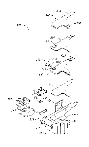
[0105] Referring now to FIG. 2, therein illustrated is an exploded
view of a portion
of a transmission line circuit assembly 200 according to various exemplary
embodiments. The transmission line circuit assembly includes a conductive
enclosure
for housing at least the transitional portion 124 of the transmission line
trace. For
example, the enclosure provides an electromagnetic cage, thereby providing a
seal
against leakage from at least the transitional portion housed in the
enclosure.
[0106] According to various exemplary embodiments, the enclosure
includes an
enclosure body 208, which further has a planar bottom wall 216 and lateral
walls 224
extending transversely from the planar bottom wall 216. The enclosure body 208
defines a cavity in which can be housed at least the transitional portion 124
of the
- 20 -
CA 02875097 2014-12-15
transmission line trace. For example, the lateral walls 224 have formed
therein at least
one throughhole 232 providing fluid communication between the cavity defined
by the
enclosure body 208 and the environment outside the enclosure body 208. The at
least
one throughhole 232 is formed at a location corresponding to a location of at
least one
transitional portion 124 housed within the enclosure. For example, the
enclosure body
208 includes a throughhole 232 for each of the transitional portions 124 of
the
transmission line trace.
[0107] The enclosure further includes a top wall 240, which may be
positioned
opposite the bottom wall 216. The top wall 240 is sized to extend between the
lateral
walls 224 of the enclosure body 208 and to substantially seal the cavity
defined by the
enclosure body 208. For example, a bead of conductive epoxy 236 (FIG. 4) may
further
adhere the edges of the top wall 240 to the lateral walls 224 to further
improve the
sealing of the cavity. Sealing the cavity with the top wall 240 suppresses any
electromagnetic leakage from the cavity of the enclosure. The top wall 240
further
provides a continuous and uniform ground for the transmission line circuit
housed in the
enclosure, which further ensures signal integrity. For example, each of the
enclosure
body 208 and the top wall 240 may be formed of a conductive metal, such as
aluminum.
[0108] According to various exemplary embodiments, the top wall 240
includes at
least a first sub-portion 248 and a second sub-portion 256, which may be
shifted
laterally in a direction parallel to a plane defined by the top wall 240. The
shifting of first
and second sub-portions 248, 256 allows a planar size of the top wall 240 to
be varied.
Accordingly, when the top wall 240 is positioned opposite the bottom wall 216
to seal
the cavity of the enclosure, the at least first and second sub-portions 248,
256 may be
shifted to abut against corresponding lateral walls 224 of the enclosure body
208. The
abutting of the first and second sub-portions 248, 256 closes any gaps formed
between
edges of the top wall 240 and corresponding lateral walls 224, further
improving the
electromagnetic sealing of the cavity of the enclosure.
[0109] At least a portion of the substrate layer 100 corresponding
to a transitional
portion 124 of the transmission line trace is positioned in the cavity defined
by the
enclosure. For example, a first conductive layer 252 is disposed between the
bottom
-21-
CA 02875097 2014-12-15
wall 216 of the enclosure body 208 and a bottom surface of the substrate layer
100. For
example, the first conductive layer 252 is formed of a silver loaded adhesive.
For
example, the conductive layer 252 provides a continuous equi-potential ground
contact
between the substrate layer 100 and the enclosure. For example, the conductive
layer
252 further mechanically adheres the bottom surface of the substrate layer 100
to the
bottom wall 216 of the enclosure body 208. For example, the conductive layer
252 aids
in electromagnetically sealing the substrate layer 100 (e.g. reducing radiated
emissions
to less than 80dBi). For example, the conductive layer 252 provides relief to
mechanical
stress due to mismatching of the coefficient of thermal expansions between the
substrate layer 100 (e.g. 12 ppm/ C) and an aluminum enclosure (24 ppm/ C).
[0110] According to various exemplary embodiments, the transmission
line circuit
defined in part by the transmission line trace is a stripline circuit and a
second
conductive layer 264 is disposed between an inner surface of the top wall 240
and a top
surface 132 of the substrate layer 100. For example, the second conductive
layer 264 is
formed of the same material as the first conductive layer 252. For example,
the second
conductive layer 264 also provides a continuous equi-potential ground contact
between
the substrate layer 100 and the enclosure. For example, the second conductive
layer
264 further mechanically adheres the top surface 132 of the substrate layer
100 to an
inner surface of the top wall 240. For example, the second conductive layer
264 further
aids in electromagnetically sealing the substrate layer 100 (e.g. reducing
radiated
emissions to less than 80dBi). For example, the second conductive layer 264
provides
relief to mechanical stress due to mismatching of the coefficient of thermal
expansions
between the substrate layer 100 (e.g. 12 ppm/ C) and an aluminum enclosure (24
ppm/ C).
[0111] According to various exemplary embodiments, the transmission line
circuit
defined in part by the transmission line trace is a stripline circuit and the
enclosure
houses the whole of the substrate layer 100, including the functional portion
128 and
each of the transitional portions 124 of the transmission line trace.
[0112] According to various exemplary embodiments, the transmission
line circuit
defined in part by the transmission line trace is a microstrip circuit and the
enclosure
- 22 -
CA 02875097 2014-12-15
houses the whole of the substrate layer 100. At least the functional portion
128 of the
transmission line trace is exposed on the upper surface 132 of the substrate
layer 100.
The top wall 240 is further positioned within the cavity of the enclosure at a
height along
the lateral walls 224 to be spaced apart from the upper surface 132 of the
substrate
layer 100 to define a gap 296 therebetween (FIG. 4). For example, due to the
gap 296,
compressive forces on the top of the enclosure in a direction of the planar
bottom wall
216 are not transmitted to the transitional portion 124 and the interfacing
portion 320 of
the connecting pin 312, thereby ensuring consistency of the bond therebetween.
[0113] According to various alternative exemplary embodiments, the
transmission
line circuit defined in part by the transmission line trace is a microstrip
circuit and the
enclosure houses one of the transitional portions 124 of the substrate layer
100. The
functional portion 128 of the transmission line trace is exposed outside the
enclosure.
For example, the exemplary transmission line circuit assembly includes a
plurality of
enclosures, each housing one transitional portion 124 of the transmission line
trace.
[0114] The transmission line circuit assembly 200 further includes a
dielectric
plug 272 having a first surface 280 and a second surface 288 (FIG. 4) opposite
the first
surface 280. The first surface 280 of the dielectric plug 272 is conductively
coupled to
an inner top surface of the enclosure at a location corresponding to one of
the
transitional portions 124 of the transmission line trace. Accordingly, the
second surface
288 of the dielectric plug 272 is aligned with the transitional portion 124
when the circuit
assembly 200 is assembled. For example, a conductive epoxy layer 292 glues the
first
surface 280 of the dielectric plug 272 to the inner top surface of the
enclosure.
[0115] For example, the dielectric plug 272 is conductively coupled
to an inner
surface of the top wall 240 of the enclosure at a location such that the
second surface
288 of the dielectric plug 272 is aligned with the transitional portion 124
when the top
wall 240 is positioned opposite the bottom wall 216 to electromagnetically
seal the
enclosure. When the circuit assembly 200 is assembled, the dielectric plug 272
is
positioned along a height of the lateral walls 224 to be spaced apart from the
transitional
portion 124 of the transmission line trace to define a gap 296 therebetween in
a
direction orthogonal to a plane defined by the substrate layer 100.
- 23 -
CA 02875097 2014-12-15
[0116] According to various exemplary embodiments, the top inner
surface of the
enclosure may be recessed at the location corresponding to the transitional
portion 124
of the transmission line trace. For example, the inner surface of the top wall
240 is
recessed. For example, the recess 242 is formed by milling the inner surface
of the top
wall 240. For example, the recess of the top inner surface of the enclosure
has a size
corresponding to the size of the dielectric plug 272. The dielectric plug 272
may be
partially positioned within the recess of the top inner surface with a
heightwise portion of
the dielectric plug 272 extending from the top inner surface. Placing of the
dielectric
plug 272 within the recess aids in maintaining the positioning of the
dielectric plug 272
and its alignment with the transitional portion 124 of the transmission line
trace.
[0117] According to various exemplary embodiments, the dielectric
plug is
selected to be 0.005" thinner compared to the thickness of the substrate layer
100. For
example, the substrate layer 100 may have a thickness of 0.020". For example,
the first
surface 280 of the dielectric plug is covered with a conductive foil enabling
reliable
adhesion of the plug 272 to the inner top surface of the enclosure and the
second
ground plane. For example, second surface 288 of the plug facing the
transitional
portion 124 of the transmission line trace is exposed and free of a conductive
covering
layer.
[0118] According to various exemplary embodiments where the
substrate layer
100 includes a recess 140 (FIG. 1) exposing one of the transitional portions
124 of the
transmission line trace, the dielectric plug 272 is aligned with the recess
140. For
example, the size of the recess 140 in a direction parallel to a top surface
132 of the
substrate layer 100 substantially corresponds to the size of the dielectric
plug 272. For
example, the dielectric plug 272 partially projects into the recess 140 of the
substrate
layer 100, further ensuring alignment of the dielectric plug 272 with the
transitional
portion 124.
[0119] According to various exemplary embodiments, a dielectric plug
272 is
provided for each transitional portion 124 of the transmission line trace.
- 24 -
CA 02875097 2014-12-15
[0120] The assembly 200 further comprises at least one connecting
pin 312. For
example, the connecting pin 312 is formed of a conductive metal such as copper
or
gold. The connecting pin 312 has a generally elongated shape having an
interfacing
portion 320 and a connecting portion 328 (FIG. 4). For example, the
interfacing portion
320 and the connecting portion 328 are integrally formed. The interfacing
portion 320 is
positioned within the enclosure and is bonded to one of the transitional
portions 124 of
the transmission line trace to form an electrical connection therebetween. For
example,
the interfacing portion 320 is bonded to the transitional portion 124 of the
transmission
line trace according one of soldering, direct welding, conductive epoxy
bonding, ribbon
bonding, and wire bonding. For example, the interfacing portion 320 may be
coated with
a non-conductive layer, such as non-conductive epoxy, to electrically insulate
the
interfacing portion 320 of the connecting pin 312 from all conductive elements
of the
assembly 200 other than the transitional portion 124 and the connecting
portion 328.
For example, various conductive layers or conductive beads used to
electromagnetically
seal the enclosure may seep to various areas of the enclosure during
fabrication of the
assembly 200, and the non-conductive layer prevents electrical contact of
these seeped
materials with the interfacing portion 320 of the connecting pin 312. The
connecting
portion 328 of the connecting pin projects through one of the lateral walls
224 of the
enclosure so that a portion of the connecting portion 328 protrudes from an
outer
surface of the lateral wall 224. The protruding portion of the connecting
portion 328 of
the connecting pin 312 is connectable to an external conductor.
[0121] According to various exemplary embodiments, the transmission
line circuit
assembly 200 further includes a connector 336. For example, the connector 336
is a
field replaceable connector. For example, the connector 336 is mechanically
coupled to
a lateral wall 224 of the enclosure. The connector 336 provides a mechanical
interface
for coupling to an external connector having the external conductor. For
example, the
external connector may be a coaxial cable or a connector of another
electromagnetic
circuit or network. When the connector 336 is appropriately mechanically
coupled to the
external connector, the connecting pin 312 is electrically coupled to the
conductor of the
external connector to form a conductive path therebetween.
- 25 -
CA 02875097 2014-12-15
[0122] According to various exemplary embodiments, the assembly 200
further
includes a non-conductive bead 352 defining a hollow channel 360 (FIGS. 3A and
3B).
When the assembly 200 is assembled, the connecting portion 328 of the
connecting pin
312 projects through the hollow channel 360 and the dielectric bead 352
substantially
surrounds the connecting portion. For example, the dielectric bead 352 is
formed of
Teflon.
[0123] Referring now to FIGS. 3A and 3B, therein illustrated are an
exploded
view and a side elevation view, respectively, showing the dielectric bead 352
and the
connecting pin 312 according to various exemplary embodiments. For example,
the
connecting portion 328 of the connecting pin 312 is cylindrical and the
interfacing
portion 320 is substantially planar. For example, when the interfacing portion
320 is
bonded to the transitional portion 124 of the transmission line, the
interfacing portion
320 is oriented so that it has a substantially elongated cross-section in a
plane
perpendicular to its direction of projection.
[0124] According to various exemplary embodiments, the dielectric bead 352
is
disposed within the throughhole 232 of the lateral wall 224 of the enclosure.
An outer
surface 368 of the dielectric bead 352 contacts an inner surface of the
throughhole 232
to mechanically support the connecting pin 312 within the throughhole 232. For
example, the dielectric bead 352 provides a snug fit of the connecting pin 312
so as to
minimize displacement or vibration of the connecting pin 312 in its radial
direction (i.e.
direction orthogonal to an axis of the connecting pin). For example, an inner
surface of
the throughole 232 and the connecting portion 320 of the connecting pin forms
a coaxial
transmission line, and the inner surface represents an outer ground.
[0125] According to various exemplary embodiments, the protruding
portion of
the connecting pin 312 partially projects into the connector 336 to contact a
conducting
pin of the connector 336.
[0126] It will be appreciated that according to various exemplary
embodiments
described herein where the assembly 200 includes the non-conductive bead 352,
the
connecting pin 312 is not directly mechanically connected to the connector 336
but is
- 26 -
CA 02875097 2014-12-15
only supported by its bond to the transitional portion 124 and its positioning
in the non-
conductive bead 352. For example, by being mechanically decoupled from the
connector 336, the connecting pin 312 may be displaced or expanded in its
axial
direction independently of an axial displacement or expansion of the connector
336,
thereby reducing mechanical stresses on the connecting pin 312 and its bond to
the
transitional portion 124 of the transmission line trace. For example, such
mechanical
stresses may otherwise be introduced due to a mismatch in the coefficient of
expansion.
This reduction of mechanical stresses allows for potting of the bonding of the
interfacing
portion 320 of the connecting pin 312 to the transitional portion 124 of the
transmission
line trace without transferring significant mechanical stresses to the bond.
[0127] According to various exemplary embodiments, the connector 336
is a
SMA connector. However, it will be understood that the connector 336 may also
form a
SMK connector. For example, the connecting pin 312 and the dielectric bead 352
are
dimensioned using standard coaxial transmission line theory to provide a
matched
impedance (e.g. 50 Ohm impedance) and support the efficient electromagnetic
signal
propagation (e.g. minimizing mismatching losses and discontinuity effects)
with the
connector 336. For example, the connector 336 is a field replaceable
connector.
[0128] According to various exemplary embodiments, a conductive shim
364 may
be disposed between a coupling surface 344 of the connector 336 and an outer
surface
of the lateral wall 224 to suppress any residual leakage of electromagnetic
energy via
the connector 336 and the lateral wall 224. For example, the conductive shim
364 is a
beryllium copper shim of appropriate thickness.
[0129] According to various exemplary embodiments, the transmission
line circuit
assembly 200 further includes a dielectric filler 376, which may be located in
the gap
296 formed between the transitional portion 124 of the transmission line
circuit and the
second surface 288 of the dielectric plug. As described herein, the dielectric
filler 376
provides electromagnetic matching and tuning of the transmission line circuit
assembly
200 and the functional portion 128 of the transmission line circuit. For
example, the
dielectric filler 376 is disposed between the second surface 288 of the
dielectric plug
272 and the transitional portion 124. For example, where the substrate layer
100 is
- 27 -
CA 02875097 2014-12-15
recessed, the filler 376 fills the recess between the dielectric plug 272 and
the top
surface 108 of the first sub-layer 112.
[0130] According to various exemplary embodiments, the dielectric
filler 376 is
generally U-shaped. When the dielectric filler 376 is positioned in the gap
296 of the
assembly, two arms of the U-shaped dielectric filler 376 extend on either side
of the
interfacing portion 320 of the connecting pin and the interfacing portion 320
is
positioned in a space defined between the two arms. By not overlaying the
dielectric
filler 376 between the second surface 288 of the dielectric plug 272 and the
interfacing
portion 320 or by overlaying a thinner portion of the dielectric filler 376
therebetween,
compressive or tensile forces applied on the enclosure in a direction between
the top
wall 240 and the bottom wall 216 are suppressed and are not substantially
transmitted
to the interfacing portion 320. Accordingly, the interfacing portion 320 and
the bond with
the transitional portion 124 are shielded from mechanical forces exerted
between the
top wall 240 and the bottom wall 216. For example these mechanical forces on
the
enclosure are significant during assembly of the circuit assembly 200, and
transmission
of these forces to the bonding of the interfacing portion 320 and the
transitional portion
124 may substantially affect the electromagnetic characteristics of the bond.
It will be
appreciated that reducing the transmission of these forces provides greater
consistency
in the bonding of the interfacing portion 320 to the transitional portion 124
and greater
consistency of the overall assembly of the circuit assembly 200.
[0131] Referring now to FIG. 4, therein illustrated is a section
view of a
transitioning region of the transmission line circuit assembly 200 along the
line A-A of
FIG. 2 when the transmission line circuit assembly 200 is fully assembled
according to
various exemplary embodiments. The dielectric plug 272, the bonding of the
transitional
portion 124 of the transmission line trace with interfacing portion 320 of the
connecting
pin 312, and the gap 296 form an electromagnetic transition 400 between the
functional
portion 128 of the transmission line and an external conductor.
[0132] For example, the electromagnetic transition 400 has a matched
impedance that matches with an impedance of the functional portion 128 of the
circuit
and an impedance of the external conductor. For example, the electromagnetic
- 28 -
CA 02875097 2014-12-15
transition 400 has an impedance of 50 ohms. For example, the electromagnetic
transition 400 provides an improvement in the return loss and insertion loss
between the
functional portion 128 and an external conductor. For example, the
electromagnetic
transition 400 further provides tuning of the transmission line circuit so
that the
electromagnetic characteristics (e.g. frequency response) obtained between the
connecting pin 312 and a connecting pin 312 of another electromagnetic
transition 400,
corresponding to another transitional portion 124 of the transmission line,
are improved
or is closer to desired electromagnetic characteristics. For example, each
electromagnetic transition 400 of the transmission line circuit assembly 200
corresponds
to a port (input or output) of the transmission line circuit.
[0133]
According to various exemplary embodiments, at least one property of at
least one element of the electromagnetic transition 400 is chosen to obtain
predetermined, specific and/or desired electromagnetic characteristics of the
electromagnetic transition 400. For example, the at least one characteristic
of at least
one element of the electromagnetic transition 400 is chosen so that the
expected
electromagnetic characteristics substantially match the predetermined,
specific and/or
desired electromagnetic characteristics within acceptable tolerances. For
example,
expected electromagnetic characteristics of the electromagnetic transition 400
are
determined based on simulated electromagnetic performance of a model of an
electromagnetic transition 400. For example, the simulated electromagnetic
performance of the model of the electromagnetic transition includes modeled
scattering
parameters. For example, the model of the electromagnetic transition 400 is a
computer-generated model.
[0134]
The predetermined, specific and/or desired electromagnetic
characteristics of the electromagnetic transition 400 is chosen based on at
least one
characteristic of the functional portion 128 of the transmission line trace.
For example,
the at least one characteristic of the functional portion 128 is a simulated
electromagnetic performance of a model of a functional portion 128. For
example, the
simulated electromagnetic performance of the model of the functional portion
128
- 29 -
CA 02875097 2014-12-15
includes modeled scattering parameters. For example, the model circuit is a
computer-
generated model circuit.
[0135]
For example, predetermined, specific and/or desired electromagnetic
characteristics of the electromagnetic transition 400 are determined based on
a
measured or simulated electromagnetic performance when the electromagnetic
transition 400 is cascaded with the functional portion 128. For example, the
predetermined, specific and/or desired electromagnetic characteristics of the
electromagnetic transition 400 are determined based on a simulated
electromagnetic
performance when the model of the electromagnetic transition 400 is cascaded
with the
model of the functional portion 128. For example, the predetermined, specific
and/or
desired electromagnetic characteristics of the electromagnetic transition 400
is
determined so that the cascading of the functional portion 128 of the
transmission line
trace with the electromagnetic transmission 400 provides predetermined,
specific and/or
desired electromagnetic characteristics of the transmission line circuit
assembly 200.
For example, electromagnetic characteristics of the transmission line circuit
assembly
200 includes the frequency response between the connecting pin 312 of a first
electromagnetic transition 400 representing a first transitional portion and
the
connecting pin 312 of a second electromagnetic transition 400 representing a
second
transitional portion, which may represent port-to-port frequency response.
[0136]
The at least one property of at least one element of the electromagnetic
transition 400 is chosen so that signal integrity is conserved between the
electromagnetic transition 400 and the functional portion 128 when the two are
cascaded. The at least one property of at least one element of the
electromagnetic
transition 400 may be further chosen to minimize discontinuity effects between
the
electromagnetic transition 400 and the functional portion 128. For example,
such
discontinuity effects may otherwise distort the performance of the cascaded
electromagnetic transition 400 and the functional portion 128 of the
transmission line
trace.
[0137]
According to various exemplary embodiments, the at least one property of
at least one element of the electromagnetic transition 400 includes the type
of material
- 30 -
CA 02875097 2014-12-15
for filing the gap 296. The type of material for filling the gap 296 may be
chosen based
on dielectric constant of the material, dissipation factor of the material, or
a combination
thereof. For example, the gap 296 is filled with a material having a
dielectric constant of
approximately 1, such as air or vacuum. Alternatively, the gap 296 is filled
with a
dielectric filler 376 formed of a material having a dielectric constant
substantially greater
than 1. For example, the dielectric filler 376 is chosen from laminate
material, glass
reinforced laminate material, ceramic loaded laminate material, PTFE-based
microwave
laminate, liquid crystal polymer, ceramic based material, plastic based
material, epoxy,
silicone, acrylic and polyurethane coating. For example, the dielectric filler
376 is formed
of a material having a dielectric constant that is substantially different
from the material
forming the substrate layer 100. For example, electromagnetic performance of
the
functional portion 128 of the transmission line trace is simulated and
predetermined,
specific and/or desired electromagnetic characteristics of the electromagnetic
transition
400 are determined based on the simulated performance.
[0138] Expected electromagnetic characteristics of electromagnetic
transitions
400 having each a dielectric filler 376 formed of different materials are
obtained.
Dielectric filler materials that provide acceptable matching of the expected
electromagnetic characteristics to the predetermined, specific and/or desired
electromagnetic characteristics are chosen as acceptable dielectric fillers
376 for the
electromagnetic transition 400 of the transmission line circuit assembly 200.
For
example, an acceptable dielectric filler 376 includes a dielectric filler 376
that when
applied in a modeled electromagnetic transition 400 that is cascaded with a
modeled
functional portion 128 of the transmission line trace causes the transmission
line circuit
assembly 200 to have the predetermined, specific and/or desired
electromagnetic
characteristics of the transmission line circuit assembly 200.
[0139] According to various exemplary embodiments, in addition to
the type of
material for filling the gap 296, the at least one property of at least one
element of the
electromagnetic transition 400 includes an amount of the dielectric filler
376. For
example, the amount of dielectric filler 376 may be defined by a thickness of
the filler
376 in a direction between the second surface 288 of the dielectric plug 272
and the
- 31 -
CA 02875097 2014-12-15
transitional portion 124. For example, electromagnetic performance of the
functional
portion 128 of the transmission line trace is simulated and predetermined,
specific
and/or desired electromagnetic characteristics of the electromagnetic
transition 400 are
determined based on the simulated performance.
[0140] Expected electromagnetic characteristics of electromagnetic
transitions
400 having each a different combination of filler material type and filler
amount are
obtained. Combinations that provide acceptable matching of the expected
electromagnetic characteristics to the predetermined, specific and/or desired
electromagnetic characteristics are chosen as acceptable combinations the
dielectric
filler material and dielectric filler amount for the electromagnetic
transition 400 of the
transmission line circuit assembly 200. For example, an acceptable combination
of the
dielectric filler material and dielectric filler amount includes a combination
that when
applied in a modeled electromagnetic transition 400 that is cascaded with a
modeled
functional portion 128 of the transmission line trace causes the transmission
line circuit
assembly 200 to have the predetermined, specific and/or desired
electromagnetic
characteristics of the transmission line circuit assembly 200.
[0141] According to various exemplary embodiments, the at least one
property of
at least one element of the electromagnetic transition 400 includes the
thickness of the
dielectric plug 272. It will be appreciated that varying the thickness of the
dielectric plug
272 further changes the distance of the gap 296 between the second surface of
the
dielectric plug 272 and the transitional portion 124 of the dielectric plug
272. For
example, electromagnetic performance of the functional portion 128 of the
transmission
line trace is simulated, and predetermined, specific and/or desired
electromagnetic
characteristics of the electromagnetic transition 400 are determined based on
the
simulated performance.
[0142] Expected electromagnetic characteristics of electromagnetic
transitions
400 having each a dielectric plug 272 of a different thickness are obtained.
The
thickness of the dielectric plug 272 that provides acceptable matching of the
expected
electromagnetic characteristics to the predetermined, specific and/or desired
electromagnetic characteristics is chosen as acceptable thickness of the
dielectric plug
- 32 -
CA 02875097 2014-12-15
272 for the electromagnetic transition 400 of the transmission line circuit
assembly 200.
For example, an acceptable thickness of the dielectric plug 272 includes a
dielectric
plug 272 that when applied in a modeled electromagnetic transition 400 that is
cascaded with a modeled functional portion 128 of the transmission line trace
causes
the transmission line circuit assembly 200 to have the predetermined, specific
and/or
desired electromagnetic characteristics of the transmission line circuit
assembly 200.
[0143] According to various exemplary embodiments, the at least one
property of
at least one element of the electromagnetic transition 400 includes the type
of material
forming the dielectric plug 272. The material forming the dielectric plug 272
may be
chosen based on dielectric constant of the material, dissipation factor of the
material, or
a combination thereof. For example, the dielectric plug 272 is formed of a
material
having a dielectric constant that is substantially equal to the dielectric
constant of the
material of the substrate layer 100. Alternatively, the dielectric plug 272 is
formed of a
material having a dielectric constant that is substantially different from the
material
forming the substrate layer 100. For example, the material forming the
dielectric plug
272 is chosen from laminate material, glass reinforced laminate material,
ceramic
loaded laminate material, PTFE-based microwave laminate, liquid crystal
polymer,
ceramic based material, plastic based material, epoxy, silicone, acrylic and
polyurethane coating. According to various exemplary embodiments, the
dielectric filler
376 and the dielectric plug 272 may be formed of the same material. For
example, the
dielectric filler 376 and the dielectric plug 272 may be contiguous.
[0144] For example, electromagnetic performance of the functional
portion 128 of
the transmission line trace is simulated and predetermined, specific and/or
desired
electromagnetic characteristics of the electromagnetic transition 400 are
determined
based on the simulated performance. Expected electromagnetic characteristics
of
electromagnetic transitions 400 having each a dielectric plug 272 formed of a
different
materials are obtained, and dielectric plug materials that provide acceptable
matching of
the expected electromagnetic characteristics to the predetermined, specific
and/or
desired electromagnetic characteristics are chosen as acceptable dielectric
plug
materials for the electromagnetic transition 400 of the transmission line
circuit assembly
- 33 -
CA 02875097 2014-12-15
200. For example, an acceptable dielectric plug material includes a type of
dielectric
plug material that when applied in a modeled electromagnetic transition 400
that is
cascaded with a modeled functional portion 128 of the transmission line trace
causes
the transmission line circuit assembly 200 to have the predetermined, specific
and/or
desired electromagnetic characteristics of the transmission line circuit
assembly 200.
[0145] Referring now to FIGS. 5, 6, and 7, therein illustrated are
perspective
views of models of three transitional portions according to various exemplary
embodiments. For example, the at least one property of at least one element of
the
electromagnetic transition 400 includes a shape of transitional portion 124 of
the
transmission line trace. For example, a width of the transitional portion 124
in a direction
transverse to the axis of the connecting pin 312 is variable along the length
of the
transitional portion 124. For example, the variable width defines at least one
matching
element 408 that causes a change in the electromagnetic characteristics of the
transmission line trace. For example, the at least one matching element 408
may be
one or more of a stub, notch, T-shape, offset T-shape, S-shape, or other known
matching elements or a combination thereof.
[0146] For example, FIG. 5 illustrates a transitional portion having
a matching
element 408 being a lateral stub.
[0147] For example, FIG. 6 illustrates a transitional portion having
a matching
element 408 being a T-shape.
[0148] For example, FIG. 7 illustrates a transitional portion having
a matching
element 408 being notches defined by portions of the transitional portions
having a
smaller width.
[0149] For example, electromagnetic performance of the functional
portion 128 of
the transmission line trace is simulated, and predetermined, specific and/or
desired
electromagnetic characteristics of the electromagnetic transition 400 are
determined
based on the simulated performance. Expected electromagnetic characteristics
of
electromagnetic transitions 400 having each a transitional portion 124 having
a different
set of dimensions are obtained, and the transitional portions corresponding to
the sets
- 34 -
CA 02875097 2014-12-15
of dimensions that provides acceptable matching of the expected
electromagnetic
characteristics to the predetermined, specific and/or desired electromagnetic
characteristics is chosen as acceptable transitional portions 124 for the
electromagnetic
transition 400 of the transmission line circuit assembly 200. For example, an
acceptable
dimensions of the transitional portion 124 includes a dimensions that when
applied in a
modeled electromagnetic transition 400 that is cascaded with a modeled
functional
portion 128 of the transmission line trace causes the transmission line
circuit assembly
200 to have the predetermined, specific and/or desired electromagnetic
characteristics
of the transmission line circuit assembly 200.
[0150] According to various exemplary embodiments, the at least one
property of
at least one element of the electromagnetic transition 400 includes at least
two of the
shape of the transitional portion 124, material for the dielectric filler 376,
amount of the
dielectric filler 376, the thickness of the dielectric plug 272 and the
material of the
dielectric plug 272. For example, electromagnetic performance of the
functional portion
128 of the transmission line trace is simulated and predetermined, specific
and/or
desired electromagnetic characteristics of the electromagnetic transition 400
are
determined based on the simulated performance.
[0151] Expected electromagnetic characteristics of electromagnetic
transitions
400 having each a different combination of at least two of the shape of the
transitional
portion 124, material for the dielectric filler 376, amount of the dielectric
filler 376, the
thickness of the dielectric plug 272 and the material of the dielectric plug
272 are
obtained. Combinations that provide acceptable matching of the expected
electromagnetic characteristics to the predetermined, specific and/or desired
electromagnetic characteristics are chosen as acceptable combinations of at
least two
of the shape of the transitional portion 124, material for the dielectric
filler 376, amount
of the dielectric filler 376, the thickness of the dielectric plug 272 and the
material of the
dielectric plug 272 for the electromagnetic transition 400 of the transmission
line circuit
assembly 200. For example, an acceptable combination includes a combination
that
when applied in a modeled electromagnetic transition 400 that is cascaded with
a
modeled functional portion 128 of the transmission line trace causes the
transmission
- 35 -
CA 02875097 2014-12-15
line circuit assembly 200 to have the predetermined, specific and/or desired
electromagnetic characteristics of the transmission line circuit assembly 200.
[0152] According to various exemplary embodiments of a process for
forming the
transmission line circuit assembly 200, the principal electromagnetic behavior
of the
transmission line circuit assembly 200 is selected. A model of a functional
circuit
providing the principal electromagnetic behavior is then generated and the
electromagnetic performance of the functional circuit model is simulated. For
example, a
full wave electromagnetic simulation may be performed to extract S-parameters
of the
electromagnetic performance of the functional circuit model. For example, the
model
may correspond to the functional portion 128 of a transmission line circuit
that has yet to
be formed. Alternatively, the model may correspond to the functional portion
128 of a
transmission line trace that has already been formed on a substrate layer 100.
[0153] According to various exemplary embodiments, a model of a
first
electromagnetic transition 400 having a known first set of properties that
includes the
shape of the transitional portion 124, material for the dielectric filler 376,
amount of the
dielectric filler 376, thickness of the dielectric plug 272 and the material
of the dielectric
plug 272 is generated. The model of the first electromagnetic transition 400
is then
cascaded with the model of the functional circuit and the electromagnetic
performance
of the cascaded configuration is simulated. A model of a second
electromagnetic
transition 400 is generated, wherein the second electromagnetic transition has
a known
second set of properties wherein at least one of the shape of the transitional
portion
124, material for the dielectric filler 376, amount of the dielectric filler
376, thickness of
the dielectric plug 272 and the material of the dielectric plug 272 has been
changed
from the first set of properties of the first electromagnetic transition
model. The model of
the second electromagnetic transition 400 is then cascaded with the model of
the
functional circuit and the electromagnetic performance of the second cascaded
configuration is simulated. The simulated electromagnetic performance is
further
compared with the simulated performance of the first cascaded configuration.
[0154] For example, performance may be compared based on at least
one of a
return loss and an insertion loss. For example, lower return loss or insertion
loss
- 36 -
CA 02875097 2014-12-15
indicates better performance. Models of additional electromagnetic transitions
having
varying properties of the shape of the transitional portion 124, material for
the dielectric
filler 376, amount of the dielectric filler 376, thickness of the dielectric
plug 272 and the
material of the dielectric plug 272 can be further generated, their
performance simulated
and compared with the performance of previously generated electromagnetic
transition
models. Accordingly, an optimization of the properties of elements of the
electromagnetic transition is carried out to determine a set of properties of
elements of
the electromagnetic transition that provides acceptable or improved
electromagnetic
performance for a given application. Accordingly, the process includes
choosing at least
one of a shape or dimensions of the transitional portion, material forming the
dielectric
filler, amount of the dielectric filler, thickness of the dielectric plug and
material of the
dielectric plug based on the simulated performance of the modeled cascaded
transmission line circuit. The set of properties of elements of the acceptable
modeled
electromagnetic transition may be then used for fabricating the
electromagnetic
transition of a transmission line circuit assembly 200 to be used in the
field.
[0155] According to various exemplary embodiments, a first
electromagnetic
transition 400 having a known first set of is properties that includes the
shape of the
transitional portion 124, material for the dielectric filler 376, amount of
the dielectric filler
376, thickness of the dielectric plug 272 and the material of the dielectric
plug 272 is
generated and cascaded to a first region of the functional circuit and a
second
electromagnetic transition having a known second set of properties that
includes the
shape of the transitional portion 124, material for the dielectric filler 376,
amount of the
dielectric filler 376, thickness of the dielectric plug 272 and the material
of the dielectric
plug 272 is generated and cascaded to a second region of the functional
circuit.
Accordingly, the first electromagnetic transition model represents a first
port of the
functional circuit and the second electromagnetic transition model represents
a second
of the functional circuit.
[0156] Further, the electromagnetic performance simulated corresponds
to port-
to-port electromagnetic characteristics (e.g. frequency response) of the
cascaded
functional circuit. An optimization can then be carried out by varying at
least one
- 37 -
CA 02875097 2014-12-15
property of the elements of either one or both of the first electromagnetic
transition
model and the second electromagnetic transition model. The simulated
performance of
the altered cascaded configuration is then compared against the simulated
performance
of a previously modeled cascaded configuration to determine a set of
properties of the
first electromagnetic transition and second electromagnetic model that will
provide an
acceptable electromagnetic performance for a given application.
[0157] Accordingly, the process includes choosing at least one of a
shape or
dimensions of the transitional portion, material forming the dielectric
filler, amount of the
dielectric filler, thickness of the dielectric plug and material of the
dielectric plug based
on the simulated port-to-port frequency response of the modeled cascaded
transmission
line circuit. The set of properties of elements of the first and second
acceptable modeled
electromagnetic transitions may be then used for fabricating the
electromagnetic
transitions of a transmission line circuit assembly 200 to be used in the
field.
[0158] According to various exemplary processes for fabricating the
transmission
line circuit assembly 200, a dielectric substrate is provided and a
transmission line trace
is formed thereon. Accordingly, a substrate layer 100 is fabricated. For
example, the
transmission line trace has a functional portion 128 and at least one
transitional portion
124 corresponding to the modeled functional circuit and the modeled at least
one
electromagnetic transition. For example, the at least one transitional portion
124 has
dimensions corresponding to the acceptable dimensions determined from the
optimization of the set of properties of the at least one electromagnetic
transition.
[0159] According to various exemplary embodiments where the
substrate layer
100 is a stripline circuit, a recess may be formed at a region corresponding
to at least
one of the transitional portions 124 to expose the transitional portion.
[0160] According to various exemplary processes for fabricating the
transmission
line circuit assembly 200, at least the transitional portion of the fabricated
substrate
layer 100 is disposed within the cavity of a metallic enclosure. For example,
the at least
one transitional portion 124 is aligned with a throughhole 232 of a lateral
wall 224 of the
- 38 -
CA 02875097 2014-12-15
enclosure. A bottom surface of the substrate layer 100 is adhered to a bottom
wall 216
of the enclosure, whereby the bottom wall 216 forms a ground plane.
[0161] A connecting pin 312 is inserted through the throughhole 232.
For
example, the connecting pin 312 may be wrapped in the non-conductive bead 352
and
supported within the throughhole 232. The interfacing portion 320 of the
connecting pin
312 is then bonded to the transitional portion 124. For example, the exemplary
process
further includes coating the interfacing portion 320 with a non-conductive
layer.
[0162] According to various exemplary processes where it is
determined from the
optimization of the set properties of the at least one electromagnetic
transition that a
dielectric filler 376 is to have a dielectric constant greater than 1, the
process further
includes disposing the dielectric filler 376 over the transitional portion 124
of the
transmission line trace. The material of the dielectric filler 376 and the
amount (e.g.
thickness) is chosen according to the acceptable filler material and amount
determined
from the optimization of the set of properties of the at least one
electromagnetic
transition.
[0163] According to various exemplary processes, a dielectric plug
272 is
fabricated. For example, the dielectric plug is formed of a material and has a
thickness
chosen according to acceptable materials and/or thicknesses determined from
the
optimization of the set of properties of the at least one electromagnetic
transition. A first
surface of the dielectric plug 272 is then adhered to an inner surface of a
top wall. For
example, the process further includes milling a recess in the inner surface of
the top
wall having a size substantially corresponding to the size of the plug 272.
[0164] According to various exemplary embodiments, the top wall is
inserted into
the cavity of the enclosure and mechanically compressed towards the bottom
wall.
Accordingly, the top wall electromagnetically seals the enclosure and the
dielectric plug
272 is aligned with and spaced apart from the transitional portion 124 of the
transmission line to define the gap 296.
- 39 -
CA 02875097 2014-12-15
[0165] According to various exemplary embodiments, the process may
further
include mechanically coupling a connector 336 to an outer wall of the metallic
enclosure, the connecting portion of the pin 312 being aligned with the
connector 336.
[0166] According to various exemplary embodiments of the
transmission line
circuit assembly 200 described herein and formed according to exemplary
processes
described herein, the dominant mode of propagation of a signal is conserved
between
the transitional portion 124 and the functional portion 128 of the
transmission line trace.
Furthermore, properties of the electromagnetic transition that provide
matching and
tuning of the functional portion 128 may be determined according to
electromagnetic
simulation prior to fabrication, thereby substantially reducing the amount of
in-vivo
turning required during and after fabrication.
EXPERIMENTS
[0167] Five electromagnetic transitions, each having a different
experimental set
of properties where modeled. The simulated electromagnetic performance was
obtained
for each of the five modeled electromagnetic transitions. Physical
electromagnetic
transitions were then fabricated according to each experimental set of
properties.
Electromagnetic performances for the five fabricated electromagnetic
transitions were
compared against the simulated electromagnetic performances.
[0168] The five experimental sets of properties of the modeled and
fabricated
electromagnetic transitions are set out in Table 1.
Variable Parameter First set Second Third set
Fourth Fifth set
set set
Dielectric Plug Thickness, (mils) 15 15 20 15 20
Plug dielectric constant 2.94 2.94 4.2 2.94 2.7
Bottom Substrate Height, (mils) 20 20 20 20 20
Void region Gap, (mils) 7 7 7
Substrate Dielectric Constant, Es 2.94 2.94 2.94 2.94
2.94
Gap Dielectric Constant, Eqap 1 4.2 4.2 2.7 2.7
Trace Width, W (mils) 32 24 23 24 23
TABLE 1
-40-
CA 02875097 2014-12-15
[0169] According to the first experimental set of properties, the
modeled and
fabricated electromagnetic transitions have a void region gap 296 that is
filled with
air/vacuum (Egap...1).
[0170] According to the second experimental set of properties, the
modeled and
fabricated electromagnetic transitions have a gap 296 that is filled with a
dielectric filler
376 having a dielectric constant of about 4.2. The void region gap of Table 1
corresponds to a distance between a top surface of the transitional portion
124 of the
transmission line trace and a bottom surface 288 of the dielectric plug 272.
[0171] According to the third experimental set of properties, the
modeled and
fabricated electromagnetic transitions is filled between the transitional
portion 124 and
an inner top surface of the enclosure with a dielectric material having a
dielectric
constant of about 4.2. For example, the dielectric plug 272 is chosen to be
formed of a
material having a dielectric constant of 4.2 and the dielectric filler 376
filling the gap 296
has a dielectric constant of about 4.2.
[0172] According to the fourth experimental set of properties, the modeled
and
fabricated electromagnetic transitions have a gap 296 that is partially filled
with a
dielectric filler 376 having a dielectric constant of about 2.7.
[0173] According to the fifth experimental set of properties, the
modeled and
fabricated electromagnetic transitions is filled between the transitional
portion 124 and
an inner top surface of the enclosure with a dielectric material having a
dielectric
constant of about 2.7. For example, the dielectric plug 272 is chosen to be
formed of a
material having a dielectric constant of about 2.7 and the dielectric filler
376 filling the
gap 296 has a dielectric constant of about 2.7.
[0174] FIG. 8 illustrates insertion loss, return loss and impedance
plots of the
simulated electromagnetic performance of the first modeled electromagnetic
transition
having the first experimental set of properties. The simulated performance
shows a
return loss of better than -25dB over a wide range of frequencies. The
insertion loss is
in the better than 0.2dB in a frequency range of up to 12GHz and increases to
0.4dB at
22 GHz.
-41-
CA 02875097 2014-12-15
[0175]
FIG. 9 illustrates insertion loss, return loss and impedance plots of the
simulated electromagnetic performance of the second modeled electromagnetic
transition having the second experimental set of properties. The simulated
performance
shows a return loss of better than -30dB over a wide range of frequencies. The
insertion
loss is in the better than 0.1dB in a wide range of frequencies.
[0176]
FIG. 10 illustrates insertion loss, return loss and impedance plots of the
simulated electromagnetic performance of the third modeled electromagnetic
transition
having the third experimental set of properties. The simulated performance
shows a
return loss of better than -30dB over a wide range of frequencies. The
insertion loss is
in the better than 0.2dB in a frequency range of up to 15GHz and increases to
0.3dB at
23GHz.
[0177]
FIG. 11 illustrates insertion loss, return loss and impedance plots of the
simulated electromagnetic performance of the fourth modeled electromagnetic
transition
having the fourth experimental set of properties. The simulated performance
shows a
return loss of better than -40dB over a wide range of frequencies. The
insertion loss is
in the better than 0.02dB in a wide range of frequencies.
[0178]
FIG. 12 illustrates insertion loss, return loss and impedance plots of the
simulated electromagnetic performance of the fifth modeled electromagnetic
transition
having the fifth experimental set of properties. The simulated performance
shows a
return loss of better than -30dB over a wide range of frequencies. The
insertion loss is
in the better than 0.03dB over a wide range of frequencies.
[0179]
FIG. 13 illustrates insertion loss plots of the simulated electromagnetic
performance of the first modeled electromagnetic transition and a measured
electromagnetic performance of a first physical electromagnetic transition
fabricated
according to the first experimental set of properties being applied to the
input and output
ports of a C band Wilkinson power divider. It will be appreciated that the
measured
insertion loss of the fabricated cascaded Wilkinson power divider and
electromagnetic
transition substantially corresponds to the simulated insertion loss of the
modeled
Wilkinson power divider and electromagnetic transition.
-42 -
CA 02875097 2014-12-15
[0180] FIG.
14 illustrates output port return loss plots of the simulated
electromagnetic performance of the first modeled electromagnetic transition
and a
measured electromagnetic performance of a first physical electromagnetic
transition
fabricated according to the first experimental set of properties being applied
to the input
and output ports of a C band Wilkinson power divider. It will be appreciated
that the
measured output port return loss of the fabricated cascaded Wilkinson power
divider
and electromagnetic transition is lower (better) than the corresponding
simulated return
loss of the modeled Wilkinson power divider and electromagnetic transition in
a wide
range of frequencies.
[0181] FIG. 15
illustrates input port return loss plots of the simulated
electromagnetic performance of the first modeled electromagnetic transition
and a
measured electromagnetic performance of a first physical electromagnetic
transition
fabricated according to the first experimental set of properties being applied
to the input
and output ports of a C band Wilkinson power divider. It will be appreciated
that the
measured input port return loss of the fabricated cascaded Wilkinson power
divider and
electromagnetic transition is lower (better) than the corresponding simulated
return loss
of the modeled electromagnetic transition.
[0182] FIG.
16 illustrates phase balance plots of the simulated electromagnetic
performance of the first modeled electromagnetic transition and a measured
electromagnetic performance of a first physical electromagnetic transition
fabricated
according to the first experimental set of properties being applied to the
input and output
ports of a C band Wilkinson power divider.
[0183] FIG.
17 illustrates isolation plots of the simulated electromagnetic
performance of the first modeled electromagnetic transition and a measured
electromagnetic performance of a first physical electromagnetic transition
fabricated
according to the first experimental set of properties being applied to the
input and output
ports of a C band Wilkinson power divider.
[0184] FIG.
18 illustrates isolation plots of the simulated electromagnetic
performance of the first modeled electromagnetic transition and a measured
-43-
CA 02875097 2014-12-15
electromagnetic performance of a first physical electromagnetic transition
fabricated
according to the first experimental set of properties being applied to the
input and output
ports of a Ku band Wilkinson power divider.
[0185] FIG. 19 illustrates phase balance plots of the simulated
electromagnetic
performance of the first modeled electromagnetic transition and a measured
electromagnetic performance of a first physical electromagnetic transition
fabricated
according to the first experimental set of properties being applied to the
input and output
ports of a Ku band Wilkinson power divider.
[0186] FIG. 20 illustrates input port return loss plots of the
simulated
electromagnetic performance of the first modeled electromagnetic transition
and a
measured electromagnetic performance of a first physical electromagnetic
transition
fabricated according to the first experimental set of properties being applied
to the input
and output ports of a Ku band Wilkinson power divider. It will be appreciated
that the
measured input port return loss of the fabricated cascaded Wilkinson power
divider and
electromagnetic transition is lower (better) than the corresponding simulated
return loss
of the modeled electromagnetic transition.
[0187] FIG. 21 illustrates output port return loss plots of the
simulated
electromagnetic performance of the first modeled electromagnetic transition
and a
measured electromagnetic performance of a first physical electromagnetic
transition
fabricated according to the first experimental set of properties being applied
to the input
and output ports of a Ku band Wilkinson power divider. It will be appreciated
that the
measured output port return loss of the fabricated cascaded Wilkinson power
divider
and electromagnetic transition is lower (better) than the corresponding
simulated return
loss of the modeled electromagnetic transition.
[0188] FIG. 22 illustrates isolation plots of the simulated
electromagnetic
performance of the first modeled electromagnetic transition and a measured
electromagnetic performance of a first physical electromagnetic transition
fabricated
according to the first experimental set of properties being applied to the
input and output
ports of a Ku band Wilkinson power divider.
-44 -
CA 02875097 2014-12-15
[0189] FIG. 23 illustrates insertion loss plot of the simulated
electromagnetic
performance of a modeled K band 2 way Wilkinson stripline power divider having
the
third modeled electromagnetic transitions.
[0190] FIG. 24 illustrates return loss plot of the simulated
electromagnetic
performance of a modeled K band 2 way Wilkinson stripline power divider having
the
third modeled electromagnetic transitions.
[0191] Experimental Wilkinson power dividers at L band, C Band, Ku
band and K
band were also constructed and validated by applying various exemplary
embodiments
described herein. It will be understood that the various exemplary embodiments
described herein may be further extended to N way power dividers (N=3,4,6,8),
quadrature couplers filters as well as active networks realized in stripline
or microstrip
technology over a wide frequency range ( 100 MHz through to 33 GHz).
[0192] While the above description provides examples of the
embodiments, it will
be appreciated that some features and/or functions of the described
embodiments are
susceptible to modification without departing from the spirit and principles
of operation
of the described embodiments. Accordingly, what has been described above has
been
intended to be illustrative of the invention and non-limiting and it will be
understood by
persons skilled in the art that other variants and modifications may be made
without
departing from the scope of the invention as defined in the claims appended
hereto.
- 45 -