Note : Les descriptions sont présentées dans la langue officielle dans laquelle elles ont été soumises.
CA 02875190 2014-12-15
TITLE OF THE INVENTION
SEMICONDUCTOR LASER LIGHT SOURCE
BACKGROUND OF THE INVENTION
Field of the Invention
The present invention relates to a light source including a semiconductor
laser.
Description of the Background Art
As light sources for lighting devices and display devices, replacing short-
lived
lamps, semiconductor light-emitting elements such as semiconductor laser
diodes (LD) or
light-emitting diodes (LED) have come to be used. As for this kind of
applications,
light-emitting elements corresponding to the three colors of red, green and
blue, which are
so-called the three primary colors of light, are used.
There is a limit to increasing illumination with the light of a
conventionally-used lamp, and the illumination on a screen becomes darker as
the screen
becomes larger. However, a laser light beam has such properties as high
directivity,
coherence and energy density, and therefore, a higher illumination may be
obtained by
adding a plurality of laser light beams. However, when coherent light such as
a laser
light beam is illuminated on a screen, a pattern including glaringly shiny
spots called
speckle noise is observed, and gives discomfort to those who are looking at
the screen.
The speckle noise appears due to an interference effect, which is a property
of a laser light
beam, and is a factor to lower the quality of lighting and displayed images.
Therefore, specifically when a light source includes a semiconductor laser, a
request for a higher power output and reducing the speckle noise becomes
stronger.
In order to emit a high power output laser light beam and reduce the speckle
noise, a conventional semiconductor laser light source includes two
semiconductor diode
CA 02875190 2014-12-15
2
arrays each of which has a plurality of active regions, which are laser light
beam emission
points, and each of the semiconductor diode arrays is determined to be a multi-
beam laser
diode array configured to emit a plurality of laser beams (laser light beams)
of different
properties. It is considered that increasing the active regions enables to
emit a plurality
of laser light beams, and adding these laser light beams together enables to
obtain higher
power output and multi-wavelengths (see, for example, Japanese Patent
Application
Laid-Open No. 07-211991 (1995)).
In addition, another semiconductor laser light source emits a laser light beam
with high brightness and high power output by using a fiber-coupling method
used to
optically couple light beams from a plurality of semiconductor lasers to an
optical fiber
(see, for example, Japanese Patent Application Laid-Open No. 2011-243717).
Furthermore, another semiconductor laser light source reduces the speckle
noise
by emitting lasers of different wavelengths from a semiconductor laser array
having a
plurality of light emission points (see, for example, Japanese Patent
Application
Laid-Open No. 2009-111230).
However, according to a technology described in Japanese Patent Application
Laid-Open No. 07-211991 (1995), a semiconductor laser chip including active
regions,
which are laser light beam emission points, is required to be mounted on a
semiconductor
laser block because thermal resistance should be considered, and the width of
the
semiconductor laser chip has to be increased so as to increase the active
regions and emit
a plurality of laser light beams. If the semiconductor laser block is
specified to a certain
size, there is a limit to the number of active regions that can be mounted on
the
semiconductor laser block. If the size of the semiconductor laser block is
made large,
the number of mountable active regions is increased, but there has been a
problem that the
overall structure of the semiconductor laser light source becomes large.
CA 02875190 2014-12-15
3
In addition, according to a technology described in Japanese Patent
Application
Laid-Open No. 2011-243717, by using a fiber coupling, laser light beams from a
plurality
of semiconductor laser arrays are condensed and a laser light beam with high
power
output is emitted. However, one semiconductor laser array having radiation
emitters
configured to emit laser light beams is mounted on one semiconductor laser
block, and
therefore, the number of semiconductor laser blocks is required to be
increased so as to
emit a laser light beam with higher power output. With the increase of the
number of
the semiconductor laser blocks, emitting a laser light beam with high power
output is
made possible, but there has been a problem that the semiconductor laser light
source
becomes large.
Furthermore, according to a technology described in Japanese Patent
Application Laid-Open No. 2009-111230, one semiconductor laser array having a
plurality of light emission points is mounted on one heat sink (semiconductor
laser block),
and therefore, the number of semiconductor laser blocks is required to be
increased so as
to emit a laser light beam with higher power output. With the increase of the
number of
the semiconductor laser blocks, emitting a laser light beam with high power
output is
made possible, but there has been a problem that the semiconductor laser light
source
becomes large.
SUMMARY OF THE INVENTION
It is an object of the present invention to provide a semiconductor laser
light
source which reduces the size of the device and is capable of emitting a laser
light beam
with high power output and reduced speckle noise.
A semiconductor laser light source according to the present invention includes
a
block mounted on a support base and having a plurality of surfaces, and a
plurality of
semiconductor laser chips emit laser light beams of different wavelengths,
respectively.
CA 02875190 2014-12-15
4
Each of the semiconductor laser chips is mounted on each surface of the block.
Each of the semiconductor laser chips is mounted on each surface of the block,
and therefore, a semiconductor laser light source that can obtain high power
output and
reduce speckle noise with a minimum number of components without adding any
component can be achieved. Thus, the semiconductor laser light source can be
achieved
with a minimum number of components, and therefore, it is possible to reduce
the size of
the device.
These and other objects, features, aspects and advantages of the present
invention will become more apparent from the following detailed description of
the
present invention when taken in conjunction with the accompanying drawings.
BRIEF DESCRIPTION OF THE DRAWINGS
FIG. 1 is a perspective view of a semiconductor laser light source according
to a
first preferred embodiment;
FIG. 2 is a cross-sectional view of the semiconductor laser light source
according to the first preferred embodiment;
FIG. 3 is a perspective view of a semiconductor laser light source according
to a
second preferred embodiment;
FIG. 4 is a perspective view of the semiconductor laser light source according
to the second preferred embodiment, showing a state of positioning corner
portions of LD
chips at corner portions of an LD block;
FIG. 5 is a perspective view of a semiconductor laser light source according
to a
third preferred embodiment;
FIG. 6 is a perspective view of the semiconductor laser light source according
to the third preferred embodiment, showing a state of positioning corner
portions of LD
chips at corner portions of an LD block;
CA 02875190 2014-12-15
FIG. 7 is a perspective view of a semiconductor laser light source according
to a
first variation of the third preferred embodiment;
FIG. 8 is a perspective view of a semiconductor laser light source according
to a
second variation of the third preferred embodiment; and
5 FIG. 9 is a
perspective view of a semiconductor laser light source according to a
third variation of the third preferred embodiment.
DESCRIPTION OF THE PREFERRED EMBODIMENTS
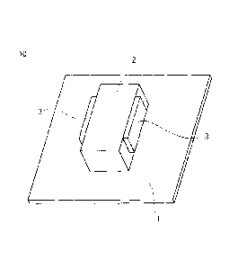
<First Preferred Embodiment>
Hereinafter, a first preferred embodiment of the present invention will be
described with reference to the drawings. FIG. 1 is a perspective view of a
semiconductor laser light source 10 according to the first preferred
embodiment, and FIG.
2 is a cross-sectional view of the semiconductor laser light source 10
according to the first
preferred embodiment.
As shown in FIGS. 1 and 2, the semiconductor laser light source 10 includes a
stem 1 (support base), a semiconductor laser block (hereinafter referred to as
an "LD
block") 2 that is a block configured to mount a semiconductor laser chip, and
a plurality
of (two, for example) semiconductor laser chips (hereinafter referred to as
"LD chips") 3.
It should be noted that electrodes for supplying currents to the LD chips 3
are omitted
because they are not directly related to the present invention.
The LD block 2 is formed into a rectangular parallelepiped shape using metal,
for example. That is, the LD block 2 has a plurality of (six) surfaces. The LD
block 2
is mounted on the stem 1 by the lower surface of the LD block 2 being fixed to
the upper
surface of the stem 1. Each surface of the LD block 2 is formed into such a
size that a
LD chip 3 can be mounted thereon. That is, each surface of the LD block 2 is
formed
into a larger size than that of the bottom surface of the LD chip 3.
CA 02875190 2014-12-15
6
The plurality of LD chips 3 emit laser light beams of different wavelengths,
respectively. The basic configuration of the semiconductor laser light source
10 has a
structure that one LD block 2 is mounted on the upper surface of the stem 1,
and the
plurality of LD chips 3 are mounted on the outer surfaces (side surfaces) of
the LD block
2. In FIGS. 1 and 2, two of the LD chips 3 are mounted on the side surfaces of
the LD
block 2, respectively. It should be noted that the plurality of LD chips 3 may
be
mounted on the four surfaces other than the upper and lower surfaces of the LD
block 2.
The conventional semiconductor laser light sources have adopted a method of
increasing the surface area or the number of LD blocks as means for emitting a
laser light
beam with high power output by adding respective laser light beams together
using the
properties of a laser light beam because one LD chip which is a laser light
beam emission
point is mounted on one LD block. With this method, there has been a problem
that the
semiconductor laser light source becomes large, and the weight of the entire
device
increases as well.
In contrast to such a conventional semiconductor laser light source, the
semiconductor laser light source 10 according to the first preferred
embodiment has a
structure capable of emitting a laser light beam with higher power output in a
small
device by mounting on one LD block 2 the plurality of LD chips 3 which emits
laser light
beams of different wavelengths, respectively and condensing each of the laser
light
beams.
Furthermore, the semiconductor laser light source 10 adds a plurality of laser
light beams of different wavelengths together, and therefore, the
semiconductor laser light
source 10 has a structure capable of emitting a laser light beam that can
obtain the effect
of speckle noise reduction as well as high power output.
Therefore, in the semiconductor laser light source 10, by mounting the
plurality
CA 02875190 2014-12-15
7
of LD chips 3 that emit laser light beams of different wavelengths on the side
surfaces of
one LD block 2, the semiconductor laser light source 10 can consequently emit
a laser
light beam with high power output and reduce the speckle noise without adding
any LD
block 2.
As described above, in the semiconductor laser light source 10 according to
the
first preferred embodiment, each of the LD chips 3 is mounted on each surface
of the LD
block 2, and therefore, the semiconductor laser light source 10 that can
obtain high power
output and reduce speckle noise with a minimum number of components without
adding
any component can be achieved. Thus, the semiconductor laser light source 10
can be
achieved by the minimum number of components, and therefore, reducing the size
of the
device is possible, and in addition, reducing manufacturing costs is also
possible.
Furthermore, the semiconductor laser light source 10 can be achieved with a
minimum
number of components, and the structure of the device does not complicate, and
therefore,
improving the yield rate of a semiconductor laser light source 10 is also
possible.
The LD block 2 is formed into a rectangular parallelepiped shape, and
therefore,
it is possible to mount the LD chips 3 on the four surfaces other than the
lower surface
that is mounted on the stem 1 and the upper surface among the six surfaces of
the LD
block 2. Thus, it is possible to mount the LD chips 3 on a maximum of four
surfaces of
the LD block 2, and therefore, it is possible to obtain higher power output
and further
reduction of the speckle noise.
It should be noted that the shape of the LD block 2 shown in FIG. 1
(rectangular
parallelepiped shape) is one example, and if the LD block has a structure
capable of
mounting the plurality of LD chips 3, the same effect can be obtained even in
a shape
other than rectangular parallelepiped.
<Second Preferred Embodiment>
CA 02875190 2014-12-15
8
A semiconductor laser light source 20 according to a second preferred
embodiment will now be described. FIG. 3 is a perspective view of the
semiconductor
laser light source 20 according to the second preferred embodiment, and FIG. 4
is a
perspective view of the semiconductor laser light source 20 according to the
second
preferred embodiment, showing a state of positioning corner portions of the LD
chips 3 at
corner portions 4d of the LD block 4. It should be noted that in the second
preferred
embodiment, the same components as those in the first preferred embodiment are
given
the same reference marks and detailed descriptions will be omitted.
As shown in FIG. 3, the semiconductor laser light source 20 includes a stem 1,
a LD block 4 mounted on the stem 1, and a plurality of (two, for example) LD
chips 3.
The LD block 4 is formed into I-shape in plan view, and includes a body
portion 4a, and
protruding portions 4b and 4c. The body portion 4a is formed into a
rectangular
parallelepiped shape, and the width of the body portion 4a is, for example,
formed smaller
than the width of the LD block 2 according to the first preferred embodiment.
In
addition, the body portion 4a includes a plurality of surfaces capable of
mounting LD
chips 3.
The protruding portions 4b and 4c protrude laterally from both end portions in
the longitudinal direction of the body portion 4a. In the LD block 4, two
corner portions
4d are formed at the boundary portion of the body portion 4a and the
protruding portion
4b, and two corner portions 4d are formed at the boundary portion between the
body
portion 4a and the protruding portion 4c. The LD chips 3 are formed into a
rectangular
parallelepiped shape, and the corner portions 4d of the LD block 4 are formed
into a
shape capable of coming into contact with the corner portions of the LD chip
3.
The basic configuration of the semiconductor laser light source 20 has a
structure configured to mount one LD block 4 on the upper surface of the stem
1 and to
CA 02875190 2014-12-15
9
mount the plurality of LD chips 3 on the outer surfaces (side surfaces) of the
body portion
4a of the LD block 4.
It is understood that a semiconductor laser light source provides higher light
utilization efficiency and enables to emit a laser light beam with high power
output by
shortening the arrangement distance of adjacent LD chips. In the LD block 2
according
to the first preferred embodiment, if the width of the LD block 2 is decreased
so as to
shorten the arrangement distance of the adjacent LD chips 3, a problem that
the LD block
2 tilts or falls over may occur before joining the lower surface of the LD
block 2 and the
stem 1.
As shown in FIG. 3, the semiconductor laser light source 20 has a structure
including protruding portions 4b and 4c which protrude laterally from both end
portions
in the longitudinal direction of the body portion 4a of the LD block 4 so that
the LD block
4 according to the second preferred embodiment does not fall over nor tilt.
Also in the
second preferred embodiment, the plurality of LD chips 3 emit laser light
beams of
different wavelengths, and thereby, the semiconductor laser light source 20
can obtain a
multi-wavelength laser light beam, and emit a laser light beam with high power
output
and reduced speckle noise.
In addition, the semiconductor laser light source requires precise alignment
of a
lens for condensing the laser light beams from the LD chips 3 and an optical
fiber, and by
precisely determining the emission point positions, that is, the positions of
the LD chips 3
as a reference of alignment, the effects are obtained that the range of
alignment is limited,
the alignment becomes easy, and in some cases the alignment becomes
unnecessary.
According to the second preferred embodiment, as shown in FIG. 4, by including
the
protruding portions 4b and 4c, positioning the corner portions of the LD chips
3 at the
corner portions 4d of the LD block 4 is easy and determining precisely
emission point
CA 02875190 2014-12-15
positions as a reference of alignment is made possible.
Furthermore, because of the LD chips 3 being precision components, when the
LD chips 3 are being mounted on the side surfaces of the body portion 4a of
the LD block
4, even if the width of the body portion 4a decreases, an operator can grasp
the protruding
5 portions 4b and 4c in the process of manufacturing the semiconductor
laser light source
20. Thereby, the operator is able to handle the LD block 4 without touching
the LD
chips 3.
As described above, in the semiconductor laser light source 20 according to
the
second preferred embodiment, the LD block 4 includes a body portion 4a with a
plurality
10 of surfaces that can mount the LD chips 3, and protruding portions 4b
and 4c that
protrude laterally from both end portions in the longitudinal direction of the
body portion
4a. Therefore, with the aim of emitting a laser light beam with higher
power output,
even if the width of the body portion 4a is decreased in order to shorten the
arrangement
distance of the adjacent LD chips 3, the LD block 4 can be prevented from
tilting or
falling over.
The LD block 4 includes the corner portions 4d capable of coming into contact
with the corner portions of the LD chip 3 at the boundary portions between the
body
portion 4a and the protruding portions 4b and 4c, and therefore, easy
alignment is
possible and an operator can handle the LD block 4 without touching the LD
chips 3 in a
manufacturing process.
It should be noted that if the protruding portions 4b and 4c have shapes
capable
of supporting the body portion 4a, and forming the corner portions 4d at the
boundary
portions of the body portion 4a and the protruding portions 4b and 4c, the
shapes are not
limited to those shown in FIGS. 3 and 4.
<Third Preferred Embodiment>
CA 02875190 2014-12-15
11
Then, a semiconductor laser light source 30 according to a third preferred
embodiment will be described. FIG. 5 is a perspective view of the
semiconductor laser
light source 30 according to the third preferred embodiment, and FIG. 6 is a
perspective
view of the semiconductor laser light source 30 according to the third
preferred
embodiment, showing a state of positioning corner portions of the LD chips 3
at corner
portions 5b of a LD block 5. It should be noted that in the third preferred
embodiment,
the same components as those in the first and second preferred embodiments are
given the
same reference marks and their detailed descriptions will be omitted.
The semiconductor laser light source 30 includes a stem 1, a LD block 5
mounted on the stern 1, and a plurality of (two, for example) LD chips 3. The
LD block
5 includes an opening portion 5a in an upward opening shape, and the opening
portion 5a
is formed by boring in the LD block in a rectangular parallelepiped shape. The
opening
portion 5a is formed into a rectangular shape in plan view.
The basic configuration of the semiconductor laser light source 30 has a
structure in which one bored LD block 5 is mounted on the upper surface of the
stem 1
and the plurality of LD chips 3 are mounted on the inner surfaces of the LD
block 5
formed by the opening portion 5a. Inside the LD block 5 four surfaces are
formed, and
each of the four surfaces is formed capable of mounting the plurality of LD
chips 3.
For higher light use efficiency and emitting a laser light beam with high
power
output, by mounting the LD chips 3 on the inner surfaces of the bored LD block
5, it is
possible to shorten further the arrangement distance of the adjacent LD chips
3 because
the LD block 5 is not disposed between the adjacent LD chips 3. In addition,
the LD
block 5 has the width of a magnitude capable of supporting itself, and
therefore, before
the lower surface of the LD block 5 joins the stem 1, such a problem that the
LD block 5
falls over or tilts does not occur.
CA 02875190 2014-12-15
12
Also according to the third preferred embodiment, the plurality of LD chips 3
emit laser light beams of different wavelengths, and thereby, the
semiconductor laser light
source 30 obtains a multi-wavelength laser light beam, and emitting a laser
light beam
with higher power output and reduced speckle noise is possible.
In addition, when the alignment positioning of the lens for condensing the
laser
light beams from the LD chips 3 and the optical fiber is performed, as shown
in FIG. 6,
positioning the corner portions of the LD chips 3 at the corner portions 5b of
the LD
block 5 is easy, and in the same manner as in the second preferred embodiment,
it is
possible to determine precisely the emission point positions as a reference of
alignment.
Furthermore, by using the LD block 5 in a manufacturing process of the
semiconductor laser light source, an operator can grasp the side portions of
the LD block
5, and therefore, in the same manner as in the second preferred embodiment, it
is possible
for the operator to handle the LD block 5 without touching the LD chips 3.
As described above, in the semiconductor laser light source 30 according to
the
third preferred embodiment, the LD block 5 is formed into an upward opening
shape and
has inside at least three surfaces that can mount LD chips 3. Therefore,
mounting the
plurality of LD chips 3 on one LD block 5 is possible, and shortening further
the
arrangement distance of the adjacent LD chips 3 is possible. Thus, the
semiconductor
laser light source 30 which can emit a laser light beam with higher power
output and
further reduce the speckle noise can be achieved.
The LD block 5 includes inside the corner portions 5b capable of coming into
contact with the corner portions of the LD chip 3, and therefore, in the same
manner as in
the second preferred embodiment, easy alignment is possible and an operator
can handle
the LD block 5 without touching the LD chips 3 in a manufacturing process. In
addition,
the LD block 5 has the width of a magnitude capable of supporting itself, and
therefore,
CA 02875190 2014-12-15
13
the LD block 5 can be prevented from tilting or falling over.
It should be noted that the shape of the LD block 5 as shown in FIGS. 5 and 6
is
one example, and if the LD block has a structure capable of mounting a
plurality of LD
chips 3 inside the LD block as shown in FIGS. 7 to 9, the same effects can be
obtained in
any shape of the LD block. FIG. 7 is a perspective view of a semiconductor
laser light
source 40 according to a first variation of the third preferred embodiment,
FIG. 8 is a
perspective view of a semiconductor laser light source 50 according to a
second variation
of the third preferred embodiment, and FIG. 9 is a perspective view of a
semiconductor
laser light source 60 according to a third variation of the third preferred
embodiment.
As shown in FIG. 7, an LD block 6 of the semiconductor laser light source 40
is
formed into a triangular shape in plan view, and includes an opening portion
6a in an
upward opening shape. The opening portion 6a is formed into a triangular shape
in plan
view. Inside the opening portion 6a, the LD block 6 includes corner portions
6b capable
of coming in contact with the corner portions of the LD chip 3. Inside the
opening
portion 6a, three surfaces are formed, and each of the three surfaces is
formed capable of
mounting the plurality of LD chips 3.
As shown in FIG. 8, an LD block 7 of the semiconductor laser light source 50
is
formed into a square shape in plan view, and includes an opening portion 7a in
an upward
opening shape. The opening portion 7a is formed into a square shape in plan
view.
The LD block 7 includes corner portions 7b capable of coming into contact with
the
corner portions of the LD chip 3 inside the opening portion 7a. Inside the
opening
portion 7a, four surfaces are formed, and each of the four surfaces is formed
capable of
mounting the plurality of LD chips 3.
As shown in FIG. 9, an LD block 8 of the semiconductor laser light source 60
is
formed into an octagonal shape in plan view, and includes an opening portion
8a in an
CA 02875190 2014-12-15
14
upward opening shape. The opening portion 8a is formed into an octagonal shape
in
plan view. The LD block 8 includes corner portions 8b capable of coming into
contact
with the corner portion of the LD chip 3 inside the opening portion 8a. Inside
the
opening portion 8a, eight surfaces are formed, and each of the eight surfaces
is formed
capable of mounting the plurality of LD chips 3.
As described above, even in the case of FIGS. 7 to 9, the same effects as in
the
case of the semiconductor laser light source 30 can be obtained.
While the invention has been shown and described in detail, the foregoing
description is in all aspects illustrative and not restrictive. It is
therefore understood that
numerous modifications and variations can be devised without departing from
the scope
of the invention.