Note : Les descriptions sont présentées dans la langue officielle dans laquelle elles ont été soumises.
CA 02875762 2014-12-04
DESCRIPTION
TITLE OF INVENTION: BURST SIGNAL RECEIVING APPARATUS
AND METHOD, PON OPTICAL LINE TERMINAL, AND PON SYSTEM
TECHNICAL FIELD
[0001] The present invention relates to a receiving apparatus and
method for receiving, for example, burst signals which are intermittently
transmitted to an optical line terminal from optical network units forming a
PON (Passive Optical Network) system, and an optical line terminal and a
PON system that use the receiving apparatus.
BACKGROUND ART
[0002] A PON system is a system in which an optical line terminal
serving as a central station is connected to optical network units installed
in
a plurality of subscribers' homes by an optical fiber network where a single
optical fiber is split into a plurality of optical fibers through an optical
coupler.
In this case, if the plurality of optical network units simultaneously
perform transmission to the optical line terminal, then transmitted data
units collide with each other. Thus, the optical line terminal provides the
optical network units with grants for a transmission timing and an amount
of transmission data. Each optical network unit performs upstream
transmission of the amount of transmission data allowed by the optical line
terminal at the timing allowed by the optical line terminal.
[0003] Since the distances between the optical line terminal and the
1
CA 02875762 2014-12-04
optical network units vary between the locations where the optical network
units are installed, the strengths of upstream optical signals received by the
optical line terminal are not uniform. Thus, upstream optical signals with
various strengths intermittently arrive at the optical line terminal from the
plurality of optical network units.
[0004] Hence, there is already proposed a technique in which, in
order to improve the reception responsivity to an optical burst signal, the
response speed of a receiving apparatus to a burst signal is changed between
a synchronization section (preamble) and a data section (payload) (see
Patent Literature 1).
In this conventional art, specifically, a small time constant is set for
the synchronization section to increase the followability for a burst signal,
and a large time constant is set for the data section to enhance the reception
tolerance to consecutive identical digits.
[00051 In addition, there is already proposed a technique in which in
order that a pre-amplifier suitable for an optical receiver module of an
optical line terminal can stably amplify a broadband burst signal, the
operating mode of the amplifier is made switchable to either a gain
adjustment mode or a gain fixed mode (see Patent Literature 2).
In this conventional art, specifically, in the adjustment mode, an
appropriate gain is determined from among two levels, based on the strength
of a burst signal in a synchronization section, and after the determination,
the burst signal is amplified in the fixed mode where the gain is fixed.
CITATION LIST
2
CA 02875762 2014-12-04
PATENT LITERATURE
[0006] Patent Literature 1: Japanese Unexamined Patent
Publication No. 2009-177577
Patent Literature 2: Japanese Unexamined Patent
Publication No. 2009-303159
SUMMARY OF INVENTION
TECHNICAL PROBLEM
[0007] In the case of Patent Literature 1, if the switching timing of
the time constant enters the data section, then a signal is received with a
small time constant set for the beginning of the data section, weakening the
reception tolerance to consecutive identical digits. Thus, the time constant
needs to be switched during the synchronization section.
In addition, in the case of Patent Literature 2, if the switching timing
of the operating mode of the pre-amplifier enters the data section, then the
beginning of the data section is not amplified by an appropriate gain. Thus,
the operating mode of the pre-amplifier needs to be switched during the
synchronization section.
[0008] Regarding this point, the optical line terminal can grasp the
arrival timing of an optical burst signal in the upstream direction from a
registered optical network unit, based on a grant determined thereby. Thus,
the optical line terminal can set the switching timings of the time constant
and the operating mode of the pre-amplifier (which may be hereinafter
collectively referred to as the "receive function") in accordance with the
synchronization section.
3
CA 02875762 2014-12-04
On the other hand, during a discovery period which takes place when
a new optical network unit is connected, the optical line terminal cannot
grasp the reception timing of an optical burst signal from the new optical
network unit, and thus, needs to determine the above-described switching
timings with reference to a time point where a burst is detected thereby.
[0009] However, the manner in which a signal rises during a period
of time (transmission ON time) from when an optical transmitter of an
optical network unit starts to transmit an optical burst signal until the
optical burst signal is turned on stably varies between the models or
manufacturers of optical network units. Thus, the time point where a burst
is detected by the optical line terminal may vary.
In this case, the switching timings of the receive function with
reference to the time point where a burst is detected also vary. Thus, there
is a problem that, when the receive function is switched at inappropriate
timings, the burst signal cannot be appropriately received.
[0010] In view of the above-described conventional problems, an
object of the present invention is to provide a receiving apparatus, etc.,
capable of appropriately receiving a burst signal having a synchronization
section, followed by a data section.
SOLUTION TO PROBLEM
[0011] (1) A receiving apparatus of the present invention is a
receiving apparatus that receives burst signals, each including a
synchronization section and a data section following the synchronization
section, from a plurality of sources in a time division manner, and includes:
4
CA 02875762 2014-12-04
an amplifying unit that amplifies each of the burst signals; a detecting unit
that detects arrival of the burst signal from an output signal from the
amplifying unit; a comparing unit that compares the output signal from the
amplifying unit with a predetermined threshold value and outputs a binary
signal; and a control unit that sets a timing of changing a receive function
during the synchronization section by adding a delay time to a detection time
point where the detecting unit performs an output, and that can change the
delay time in a plurality of ways.
[0012] According to the receiving apparatus of the present invention,
the control unit sets a timing of changing the receive function during the
synchronization section by adding a delay time to a detection time point
where the detecting unit performs an output, and can change the delay time
in a plurality of ways. Thus, by adjusting the timing of changing the receive
function by trial and error using a plurality of delay times, switching of the
receive function can be performed at an appropriate timing.
Hence, a burst signal having a synchronization section, followed by a
data section can be appropriately received.
[0013] Note that, when the receiving apparatus of the present
invention can identify a time point where a burst signal from a
predetermined transmitting apparatus (e.g., an optical network unit in
upstream communication in a PON system) is received (e.g., when the
optical network unit performs upstream transmission in accordance with a
transmission time granted by an optical line terminal in the PON system),
the receiving apparatus does not need to perform the above-described
process in which the timing of changing the receive function is adjusted by
CA 02875762 2014-12-04
trial and error.
Therefore, the receiving apparatus of the present invention needs to
perform the above-described process in which the timing of changing the
receive function is adjusted by trial and error, only when the receiving side
cannot identify a time point where a burst signal from a transmitting
apparatus is received (e.g., when it is a discovery period of a PON system).
[0014] Namely, in the receiving apparatus of the present invention,
the control unit that sets the timing of changing the receive function during
the synchronization period by adding a delay time to a detection time point
where the detecting unit performs an output needs to be able to change the
delay time only when a time point where a burst signal from a transmitting
apparatus is received cannot be identified.
In addition, in the receiving apparatus of the present invention, in
the above-described process in which the timing of changing the receive
function is adjusted by trial and error, there may be a case of failing to
receive a burst signal. However, once reception has succeeded, the timing of
changing the receive function of the burst signal can be identified
thereafter.
Thus, it is not particularly problematic.
[0015] (2) In the receiving apparatus of the present invention, it is
preferred that, when clock and data recovery based on the binary signal
cannot be performed despite a fact that the detecting unit has detected
arrival of the burst signal, the control unit change the delay time to a
different value.
By doing so, compared to the case in which the value of the delay
time is changed in fixed or random order, the possibility that a burst signal
6
CA 02875762 2014-12-04
can be appropriately received can be increased.
[0016] (3) However, the control unit may switch a value of the delay
time to a different value in fixed or random order every time the detecting
unit detects arrival of a burst signal.
By doing so, there is no need to determine whether clock and data
recovery based on a binary signal has succeeded. Thus, there is an
advantage in ease of control to change the delay time.
[0017] (4) It is preferred that the receiving apparatus of the present
invention further include a time constant circuit that can follow the output
signal from the amplifying unit at different time constants.
In this case, the time constant is included in the receive function to
be changed during the synchronization section. As the control unit, one
may be adopted that can set a timing of changing the time constant during
the synchronization section by adding the delay time to a time point where
the detecting unit performs an output, and that can change the delay time in
a plurality of ways.
[0018] (5) In addition, in the receiving apparatus of the present
invention, it is preferred that the amplifying unit include an amplifier
circuit
having, as a switchable operating mode, an adjustment mode where a gain is
adjusted according to a strength of the burst signal, and a fixed mode where
the gain is fixed.
In this case, the operating mode is included in the receive function to
be changed during the synchronization section. As the control unit, one
may be adopted that can set a timing of changing the operating mode during
the synchronization section by adding the delay time to a time point where
7
CA 02875762 2014-12-04
the detection performs an output, and that can change the delay time in a
plurality of ways.
[0019] (6) A receiving method of the present invention is a receiving
method for a case of receiving burst signals, each including a synchronization
section and a data section following the synchronization section, from a
plurality of sources in a time division manner, and includes the steps of;
detecting arrival of each of the burst signals from an amplified signal of the
burst signal; comparing the amplified signal with a predetermined threshold
value and outputting a binary signal; setting a first timing of changing a
receive function during the synchronization section by adding a first delay
time to a detection time point where the detecting unit performs an output;
and setting a second timing of changing the receive function during the
synchronization section by adding a second delay time to the detection time
point, the second delay time being different than the first delay time.
[0020] The receiving method of the present invention includes the
step of setting a timing of changing the receive function during the
synchronization section by adding a first delay time to a detection time point
where the detecting unit performs an output; and the step of setting a timing
of changing the receive function during the synchronization section by
adding a second delay time different than the first delay time to the
detection time point. Thus, by performing those steps of adjusting the
timing of changing the receive function by trial and error using the first and
second delay times, switching of the receive function can be performed at an
appropriate timing.
Hence, a burst signal having a synchronization section, followed by a
8
CA 02875762 2014-12-04
data section can be appropriately received.
[0021] Note that, in the receiving method of the present invention,
the first and second delay times are expressions focusing on two types of the
delay time with different values. Thus, the number of values of the delay
time used in the receiving method of the present invention is not limited to
two.
Therefore, the receiving method of the present invention also
includes a case in which the above-described two steps are repeated using
the values of three types or more of the delay time and the timing of
changing the receive function during the synchronization section is adjusted
three times or more.
[0022] (7) An optical line terminal of the present invention is a PON
optical line terminal including the receiving apparatus described in the
above-described (1) to (5), and provides the same functions and effects as
those provided by the receiving apparatus.
(8) In the optical line terminal of the present invention, it is preferred
that the control unit re-set the timing for a discovery period for registering
the optical network units.
[0023] The reason for that is that since, as described above, the
optical line terminal cannot pre-detect the transmission timing of a burst
signal from a new optical network unit during a discovery period, the optical
line terminal needs to determine the timing of changing the receive function
during a synchronization section, from a time point where a burst signal is
detected thereby. Thus, the utility value for when the present invention is
adopted is high.
9
CA 02875762 2014-12-04
[0024] (9) A
PON system of the present invention is a PON system
including, as a component, an optical line terminal having the receiving
apparatus described in the above-described (1) to (5), and provides the same
functions and effects as those provided by the receiving apparatus.
ADVANTAGEOUS EFFECTS OF INVENTION
[0025] As
described above, according to the present invention, a
burst signal including a synchronization section and a data section can be
appropriately received.
BRIEF DESCRIPTION OF DRAWINGS
[0026] [FIG. 1] FIG. 1 is an overall
configuration diagram of a
PON system according to an embodiment of the present invention.
[FIG. 2] FIG. 2 is a circuit
diagram of a receiver circuit
provided in an optical line terminal.
[FIG. 31 FIG. 3 is a circuit
diagram showing the
details of a time constant circuit.
[FIG. 4] FIG. 4 is an
illustrative diagram showing an
example of burst signal arrival order.
[FIG. 51 FIG. 5 is a time
chart showing a temporal
relationship between the first half portion of a burst signal, a burst
detection
signal, and the switching timings of a pre-amplifier and the time constant
circuit.
DESCRIPTION OF EMBODIMENTS
CA 02875762 2014-12-04
[0027] An embodiment of the present invention will be described
below based on the drawings.
[Overall configuration of a PON system]
FIG. 1 is an overall configuration diagram of a PON system
according to an embodiment of the present invention.
In FIG. 1, an optical line terminal (OLT) 1 is installed as a central
station for a plurality of optical network units (ONUs) 2 to 4. The optical
network units 2 to 4 are installed in PON system subscribers' homes,
respectively.
[0028] A single optical fiber 5 connected to the optical line terminal
1
is split into a plurality of optical fibers (branch lines) 7 to 9 through an
optical coupler 6 which is a passive optical splitting node. The optical
network units 2 to 4 are connected to the ends of the split optical fibers 7
to 9,
respectively.
The optical line terminal 1 is communicably connected to an upper
network 11, and the optical network units 2 to 4 are communicably connected
to their respective user networks 12 to 14.
[0029] Although FIG. 1 shows three optical network units 2 to 4, it is
possible to connect, for example, 32 optical network units by splitting an
optical fiber into 32 optical fibers through the single optical coupler 6. In
addition, although in FIG. 1 only one optical coupler 6 is used, by providing
a
plurality of optical couplers 6 longitudinally, more optical network units can
be connected to the optical line terminal 1.
Note that the distances from the optical line terminal 1 to the optical
network units 2 to 4 are not uniform, and thus, the strengths of signals
11
CA 02875762 2014-12-04
coming from the optical network units 2 to 4 are not uniform, either.
[0030] In FIG. 1, in the upstream direction from the optical network
units 2 to 4 to the optical line terminal 1, data is transmitted at wavelength
X 1.
On the other hand, in the downstream direction from the optical line
terminal 1 to the optical network units 2 to 4, data is transmitted at
wavelength X2. The wavelengths X1 and X2 are set based on, for example,
Clause 60 of IEEE Standard 802.3ah-2004 in the case of GE-PON.
[0031] In the above-described PON system, downstream
transmission from the optical line terminal 1 to the optical network units 2
to 4 is performed at any time in broadcast form. Each of the optical network
units 2 to 4 captures only those downstream frames destined therefor, and
discards other downstream frames.
On the other hand, upstream transmission from the optical network
units 2 to 4 to the optical line terminal 1 is performed under the control of
the optical line terminal 1. Each of the optical network units 2 to 4
performs upstream transmission of an amount of transmission data allowed
for transmission at a transmission time allowed (granted) for transmission
by the optical line terminal 1.
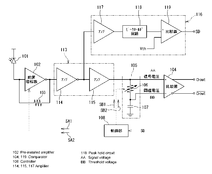
[0032] [Burst receiver circuit of the optical line terminal]
FIG. 2 is a circuit diagram of a receiver circuit (receiving apparatus)
20 provided in the optical line terminal 1.
As shown in FIG. 2, the receiver circuit 20 of the present embodiment
includes a photodiode 101, a pre-amplifier 102, a feedback resistor 103, a
post-amplifier 113, a time constant circuit 105, a comparator 104, and a
12
CA 02875762 2014-12-04
signal detector circuit 116.
[0033] Of the components, the photodiode 101 which is a light
receiving element receives an optical burst signal generated based on a
binary signal (digital signal), and converts the optical burst signal into an
electrical signal and outputs the electrical signal.
The output signal from the photodiode 101 is amplified by the
pre-amplifier 102 having the feedback resistor 103 connected between its
input and output. The amplified signal (the burst signal formed of the
electrical signal) outputted from the pre-amplifier 102 is inputted to the
post-amplifier 113 subsequent to the pre-amplifier 102.
[0034] The post-amplifier 113 includes two amplifiers 114 and 115.
The amplifiers 114 and 115 further amplify the amplitude of the burst signal
outputted from the pre-amplifier 102. The pre-amplifier 102 and the
post-amplifier 113 compose an amplifying unit that amplifies the burst
signal formed of the electrical signal outputted from the photodiode 101.
An output signal from the post-amplifier 113 is inputted as a signal
voltage to one of the input terminals of the comparator 104. In addition, a
voltage which is the burst signal outputted through the time constant circuit
105 is inputted as a threshold voltage to the other input terminal of the
comparator 104.
[0035] The time constant circuit 105 is formed of a low-pass filter
including a variable resistor 106 whose resistance value is variable by
external control; and a capacitor 107 whose one end is connected to the
resistor 106 and whose other end is the ground potential. In this case, when
the resistance value of the variable resistor 106 is R and the capacitance of
13
CA 02875762 2014-12-04
the capacitor 107 is C, the time constant t can be calculated by t = R = C.
The comparator 104 compares the signal voltage with the threshold
voltage and outputs the comparison result as a binary signal (digital signal)
Dout of 0 or 1 and a logically inverted signal thereof. The resistance value
of the resistor 106 can be changed by a control unit 108.
[0036] The signal detector circuit 116 composes a detecting unit that
detects arrival of the burst signal from an output signal from the
post-amplifier 113. The signal detector circuit 116 includes an amplifier 117,
a peak-hold circuit 118, and a comparator 119.
The input terminal of the amplifier 117 is connected between the
amplifiers 114 and 115 in the post-amplifier 113. An output signal from the
amplifier 114 is inputted to the peak-hold circuit 118. The peak-hold circuit
118 holds a maximum voltage value of the amplifier 117 and outputs the
maximum voltage value to the comparator 119 subsequent thereto.
[0037] The comparator 119 compares the held voltage value with a
predetermined threshold value (reference voltage) Vth. When the voltage
value is greater than or equal to the threshold value Vth, the comparator 119
sets a burst detection signal SD to "High". When the voltage value is less
than the threshold value Vth, the comparator 119 sets the burst detection
signal SD to "Low".
[0038] The pre-amplifier 102 can operate in either an "adjustment
mode" which is an operating mode where the gain is adjusted according to
the strength of the burst signal (electrical output) inputted thereto from the
photodiode 101 or a "fixed mode" which is an operating mode where the gain
is fixed.
14
CA 02875762 2014-12-04
As such a pre-amplifier 102 capable of switching the operating mode,
there is, for example, one shown in the above-described Patent Literature 2.
In the present embodiment, the same pre-amplifier as that one is adopted.
Note that the operating mode of the pre-amplifier 102 may have a third mode
other than those described above.
[0039] For the already registered optical network units 2 to 4, the
control unit 108 performs predetermined dynamic bandwidth allocation in
response to a request, and generates grants each including the transmission
timing and amount of transmission data of an optical burst signal to be
transmitted by each of the optical network units 2 to 4, and performs
downstream transmission of the grants to the optical network units 2 to 4.
The control unit 108 grasps the arrival times and time lengths of
synchronization sections and data sections of the optical burst signals to be
transmitted by the optical network units 2 to 4, based on the transmission
timings granted thereby to the optical network units 2 to 4.
[0040] The control unit 108 performs downstream transmission of a
discovery gate during a "discovery period" (see FIG. 4) for registering an
unregistered optical network unit (not shown). The control unit 108
provides an LLID to an optical network unit having performed upstream
transmission of a registration request in response to the discovery gate, and
thereby newly registers the optical network unit.
In addition, the control unit 108 controls the switching timing of the
operating mode of the pre-amplifier 102 by control signals SA1 and SA2, and
controls the switching timing of the time constant of the time constant
circuit
105 by control signals SB1 and SB2 (see FIG. 2).
CA 02875762 2014-12-04
[0041] Of the control signals SA1, SA2, SB1, and SB2, the control
signals SA1 and SB1 are control signals for the registered optical network
units 2 to 4, and the control signals SA2 and SB2 are control signals for
unregistered optical network units.
Namely, the control unit 108 controls the switching of the
pre-amplifier 102 and the time constant circuit 105 by the control signals
SA1 and SB1 during a normal period other than the discovery period, and
controls the switching of the pre-amplifier 102 and the time constant circuit
105 by the control signals SA2 and SB2 during the discovery period.
[0042] [Switching control of the receive function during the normal
period]
FIG. 3 is a circuit diagram showing a specific example of the time
constant circuit 105 for making the resistance value of the resistor 106
variable. FIG. 4 is an illustrative diagram showing an example of burst
signal arrival order.
As shown in FIG. 3, the time constant circuit 105 includes a series
unit of a resistor RO (resistance value RO) and the capacitor 107 which is
provided between a signal potential and the ground potential.
[0043] In addition, the time constant circuit 105 includes a series
unit of a resistor R1 (resistance value R1) connected in parallel to the
resistor RO and a switching element (e.g., a MOS-FET) 111; and likewise a
series unit of a resistor R2 (resistance value R2) connected in parallel to
the
resistor RO and a switching element 112.
Here, in EPON (IEEE 802.3ah) and 10G-EPON (IEEE 802.3av), a
burst signal is composed of the following portions 1) to 4) in this order from
16
CA 02875762 2014-12-04
:.
the beginning (see FIG. 4).
[0044] 1) Transmission ON section (TON): a time period for a
transmitter of an ONU to stably turn on a burst signal. Note, however, that
a signal waveform is not guaranteed during this section.
2) Synchronization section: a time period for a receiver of the OLT to
synchronize to the burst signal. It is also called a preamble section.
3) Data section: a time period during which data is transmitted. It
is also called a payload section.
4) Transmission OFF section (ToFF): a time period for the transmitter
of the ONU to turn off the burst signal.
[0045] With reference to FIG. 4, during the normal period,
the
control unit 108 grasps in advance time t1 at which the preamble portion
starts to be received first; time t3 at which the data portion starts to be
received first; time t4 at which the reception of the burst signal is
completed;
and time t5 at which the burst signal is turned off. In addition, the control
unit 108 also grasps in advance time t6 at which the next burst signal starts
to arrive after a no-signal section.
Hence, during the normal period, the control unit 108 switches the
time constant of the time constant circuit 105 by turning on/off the control
terminals of the switching elements 111 and 112 (e.g., the gates of
MOS-FETs) in the time constant circuit 105 by the control signal SA1 as
shown in the following table 1.
17
CA 02875762 2014-12-04
...
[0046] [Table 1]
Switching Switching Time
Control example 1 (R2 <R1)
element 111 element 112 constant
First part of Preamble section00-r-D
Off T1
_ the signal (first half)
(medium)
Preamble section
Last part of
(second half) and Off Off
T2 (long)
the signal
data section
No-signal section Off On
T3 (short)
[0047] In table 1, it is assumed that the resistance values
R1 and R2
have a relationship of R2 < R1. Different controls are performed on on/off of
the switching elements 111 and 112 for the first part and last part of the
burst signal and the no-signal section of the burst signal.
First, during a part of the synchronization section which is the first
part of the signal (time ti to t2), the switching element 111 is placed in an
on
state, and the switching element 112 is placed in an off state.
[0048] By this, when the on-resistance of the switching
element 111
is Rs1, the time constant circuit 105 is formed such that the capacitor 107
(capacitance C) is connected to parallel resistors of the resistor RO and the
resistors (R1 + Rs1). In this case, the time constant T1 is as shown in the
following equation (1):
T1 = {RO = (R1 + Rs1)/(R0 + R1 + Rs1)} - C ............... (1)
Note that time t2 can be set to a predetermined time a bit before time
t3 which is the end of the preamble.
[0049] Subsequently, during the other part of the
synchronization
section (time t2 to t3) and the data section (time t3 to t4) which are the
last
part of the signal, i.e., time t2 to t4, the switching elements 111 and 112
are
both placed in an off state. By this, the resistors R1 and R2 in the time
18
CA 02875762 2014-12-04
constant circuit 105 become invalid, resulting in a time constant of only the
resistor RO and the capacitor 107 (capacitance C). This time constant -r2 is
as shown in the following equation (2):
-c2 = RO - C ....... (2)
[0050] Subsequently, during the no-signal section (time t4 to t6), the
switching element 111 is placed in an off state and the switching element 112
is placed in an on state. By this, when the on-resistance of the switching
element 112 is Rs2, the time constant is of the resistor RO, parallel
resistors
of R2 + Rs2, and the capacitor 107 (capacitance C). This time constant T3 is
as shown in the following equation (3):
-r3 = {RO = (R2 + Rs2)/(R0 + R2 + Rs2)} = C .... (3)
[0051] In the above-described equations (1) to (3), when another
resistor (R1 or R2) is connected in parallel to the resistor RO, the
resistance
value of the entire parallel resistors is smaller than the resistor RO. In
addition, the smaller the resistance value connected in parallel, the smaller
the resistance value of the entire parallel resistors. Therefore, the
following
inequality (4) holds:
-r3 < < ... (4)
When this is represented as a relative relationship between the
lengths of the time constant, the first part of the signal is "medium", the
last
part of the signal is "long", and the no-signal section is "short".
[0052] The control unit 108 switches the time constant of the time
constant circuit 105 in the above-described manner, and sets the time
constant for the first half of the synchronization section (ti to t2) to be
relatively short. By this, the threshold voltage which is the output voltage
19
CA 02875762 2014-12-04
from the time constant circuit 105 promptly follows the median of the
preamble.
In particular, when a bit-inversion repeating signal such as 0, 1, 0, 1,
..................................................................... is used
in the preamble, since the frequency component of the signal is
high (there is only one bit of a consecutive identical symbol), by setting a
short time constant, the median can be rapidly detected. By this, the
responsivity to the burst signal is improved.
[0053] During
a period from the second half of the synchronization
section to the data section which is the last part of the signal (t2 to t4),
the
control unit 108 sets the time constant to be longer than that for the first
part of the signal, according to the encoding format in the data section. By
this, the threshold voltage in the data section is stabilized so as not to
shift
much from the center of the amplitude.
Furthermore, the control unit 108 sets the time constant to be
shortest in the no-signal section to promptly bring the threshold voltage back
to a no-signal level. Therefore, even immediately after receiving a burst
signal with high optical signal strength (amplitude), the threshold voltage
can be promptly brought back to a no-signal level and thus a no-signal period
can be reduced. Hence, the upstream communication bandwidth can be
more effectively utilized.
[0054] During
the normal period, the control unit 108 switches the
operating mode of the pre-amplifier 102 by the control signal SB1 at the
timings shown in FIG. 4.
Specifically, until the time point a bit before time t2, the control unit
108 sets the operating mode of the pre-amplifier 102 to an "adjustment
CA 02875762 2014-12-04
mode" to allow the pre-amplifier 102 to adjust the gain according to the
strength of the burst signal.
[0055] During a period after the above-described time point where
the signal strength is stabilized, the control unit 108 sets the operating
mode
of the pre-amplifier 102 to a "fixed mode" to fix the gain of the pre-
amplifier
102 at a predetermined value.
Note that at time t5 at which the burst signal is turned off, the
control unit 108 changes the fixed mode back to an "adjustment mode", and
resets the value of the output voltage held by the pre-amplifier 102 to bring
the gain back to its initial value. By this, it becomes easier to adjust the
gain for the next burst signal.
[0056] [Switching control of the receive function during the
discovery period]
FIG. 5 is a time chart showing a temporal relationship between the
first half portion of a burst signal, a burst detection signal SD, and control
signals SA2 and SB2 for the pre-amplifier 102 and the time constant circuit
105.
As described above, the optical line terminal 1 waits for upstream
transmission from an unregistered optical network unit during the discovery
period (see FIG. 4). For an optical burst signal received during the
discovery period (an optical burst signal at time t7 to t8 in FIG. 4), the
optical line terminal 1 cannot perform switching control of the pre-amplifier
102 and the time constant circuit 105 using time ti to t6 grasped in advance
thereby.
[0057] Hence, as shown in FIG. 5, the control unit 108 determines
21
CA 02875762 2014-12-04
the switching timings of the operating mode and the time constant with
reference to the burst detection signal SD outputted from the signal detector
circuit 116, and uses the determined timings as a trigger to change the states
of the control signals SA2 and SB2.
Specifically, the control unit 108 pre-stores delay times Da and Db
from a burst detection time point td0. The control unit 108 uses time ta
obtained by adding the delay time Da to the burst detection time point SD as
the switching timing of the operating mode, and uses time tb obtained by
adding the delay time Db to the burst detection time point td0 as the
switching timing of the time constant.
[0058] Namely, the control signal SA2 which is outputted to the
pre-amplifier 102 from the control unit 108 during the discovery period is a
control signal that sets the operating mode to an adjustment mode until time
ta which is obtained by adding the delay time Da to an SD rise time point tb0,
and sets the operating mode of the pre-amplifier 102 to a fixed mode after
that time ta.
In addition, the control signal SB2 which is outputted to the time
constant circuit 105 from the control unit 108 during the discovery period is
a control signal that sets the time constant of the time constant circuit 105
to
shortish "t3" until time tb which is obtained by adding the delay time Db to
the SD rise time point td0, and sets the time constant of the time constant
circuit 105 to longer "t2" after that time tb.
[0059] Note that, as shown in FIG. 5, the delay times Da and Db are
set such that both of time ta and tb are within the synchronization section
and ta < tb. By this, after the amplitude of an output signal from the
22
CA 02875762 2014-12-04
pre-amplifier 102 is stabilized, the time constant can be switched.
Meanwhile, if, as indicated by a solid line at the top of FIG. 5, the
manner in which the beginning of the burst signal rises (the form of a
transmission ON section) is sufficiently fast and has a form close to an ideal
rectangular wave, then even if the source of the burst signal is changed or
even if the reception strength of the burst signal is changed, the burst
detection time point td0 does not move forward or backward.
[0060] However, the manner in which the beginning of the burst
signal rises varies between the models or manufacturers of optical network
units. For example, as indicated by imaginary lines at the top of FIG. 5, the
burst signal may exceed the threshold value Vth at time tdl which is
substantially the center of the transmission ON section, or may exceed the
threshold value Vth at time td2 immediately before the start of the
synchronization section. In addition, as indicated by the solid line, the
burst signal may exceed the threshold value Vth at time td0 which is the
front edge of the transmission ON section.
Therefore, in practice, the rise of the burst detection signal SD often
varies forward or backward in the range of time tb0 to tb2. In this case,
time ta and tb calculated based on the SD also vary forward or backward.
[0061] In particular, when the rise of the burst detection signal SD is
delayed later than time td2, time ta and tb are also correspondingly delayed
significantly. At worst, both of time ta and tb enter the data section and
accordingly the burst signal may not be able to be appropriately received.
In view of this, in the present embodiment, a plurality of switching
timings are prepared in advance, and the switching timings are changed in
23
CA 02875762 2014-12-04
fixed order or randomly every discovery period for registering an optical
network unit. By this, the above-described problem is solved.
[0062] Specifically, the control unit 108 holds delay times Dai and
Dbi of at least two types, long and short (i=1, 2, )
The control unit 108 changes each of the held delay times Dai and
Dbi to a different value every discovery period, and thereby sets each of the
switching timings of the control signals 5A2 and SB2 to a different time
point for each discovery period.
[0063] For example, when the switching timings of the control
signals SA2 and SB2 are changed in fixed order, the control unit 108 uses
delay times Dal and Db 1 during a predetermined discovery period, and uses
delay times Da2 and Db2 during the next discovery period.
When the switching timings of the control signals 5A2 and SB2 are
changed randomly, the control unit 108 randomly selects arbitrary delay
times Dai and Dbi from among the held delay times during an arbitrary
discovery period, and randomly selects other delay times Daj and Dbj (j#i)
during the next discovery period.
[0064] [Effect of the burst receiver circuit]
As described above, according to the burst receiver circuit 20 of the
present embodiment, when the control unit 108 sets the switching timings of
the receive function (specifically, the operating mode of the pre-amplifier
102
and the time constant of the time constant circuit 105) for the
synchronization section by adding delay times Dai and Dbi to a time point
td0 to td2 at which a burst signal is detected by the signal detector circuit
116, the control unit 108 changes the timings of the switching timings by
24
CA 02875762 2014-12-04
..
adopting different sets of delay times Dai and Dbi in fixed order or randomly.
[0065] Hence, even if the burst signal arrival time point td0 to
td2
moves forward or backward, by adding a different set of delay times Dai and
Dbi, the switching timings of the control signals SA2 and SB2 can be set at
appropriate time points within the synchronization section.
Accordingly, by making a change to the receive function using a
plurality of sets of delay times Dai and Dbi a plurality of times, the receive
function can be changed at appropriate timings. Thus, the optical line
terminal 1 can appropriately receive even a burst signal that is transmitted
during a discovery period from an optical network unit that cannot set a long
synchronization section.
[0066] [First variant]
Although in the above-described embodiment the delay times Dai
and Dbi are changed in fixed or random order, a determination as to whether
to change the delay times Dai and Dbi may be made according to whether a
burst signal has been able to be appropriately received.
Specifically, a clock and data recovery circuit (CDR circuit) is
normally provided subsequent to the burst receiver circuit 20.
[0067] Hence, a signal indicating as to whether clock and data
recovery has succeeded is inputted to the control unit 108. Then, when the
control unit 108 obtains a recovery success signal from the clock and data
recovery circuit within a predetermined period of time after a burst detection
signal SD of the signal detector circuit 116 rises, the control unit 108 does
not change the delay times Dai and Dbi.
On the other hand, when the control unit 108 does not obtain the
CA 02875762 2014-12-04
above-described recovery success signal within the predetermined period of
time after the burst detection signal SD of the signal detector circuit 116
rises, the control unit 108 changes the delay times Dai and Dbi.
[0068] By doing so, compared to the case in which the values of the
delay times Dai and Dbi are changed in fixed or random order, the possibility
that reception of a burst signal can be appropriately received can be
increased.
However, when, as in the above-described embodiment, the values of
the delay times Dai and Dbi are changed in fixed or random order, there is no
need to determine from a signal from the clock and data recovery circuit
whether the recovery has succeeded. Thus, there is an advantage in ease of
control to change the delay times Dai and Dbi.
[0069] [Other variants]
The embodiment (including the above-described variant) disclosed
herein is in all respects as illustrative and not restrictive. The scope of
right of the present invention includes all changes which come within the
range of equivalency of the configurations recited in the claims, but not the
above -described embodiment.
[0070] For example, although in the above-described embodiment
the control unit 108 controls the switching timings of both of the operating
mode of the pre-amplifier 102 and the time constant of the time constant
circuit 105, the configuration may be such that the control unit 108 controls
only one of them.
In addition, in the above-described embodiment, the receive function
whose switching timings are to be controlled by the control unit 108 are not
26
CA 02875762 2014-12-04
,
limited to the operating mode of the pre-amplifier 102 and the time constant
of the time constant circuit 105.
REFERENCE SIGNS LIST
[00711 1: OPTICAL LINE TERMINAL
2 to 4: OPTICAL NETWORK UNIT
20: BURST RECEIVER CIRCUIT (RECEIVING
APPARATUS)
102: PRE-AMPLIFIER (AMPLIFYING UNIT)
104: COMPARATOR
105: TIME CONSTANT CIRCUIT
108: CONTROL UNIT
113: POST-AMPLIFIER (AMPLIFYING UNIT)
114: AMPLIFIER
115: AMPLIFIER
116: SIGNAL DETECTOR CIRCUIT (DETECTING UNIT)
27