Note : Les descriptions sont présentées dans la langue officielle dans laquelle elles ont été soumises.
CA 02877904 2014-12-24
WO 2014/004364
PCT/US2013/047287
LARGE AREA ORGANIC PHOTOVOLTAICS
Cross-Reference to Related Applications
[001] This application claims the benefit of U.S. Provisional Application
No. 61/664,058 filed June 25, 2012, which is incorporated herein by reference
in its entirety.
Statement Regarding Federally Sponsored Research
[002] This invention was made with Government support under DE-EE0005310
awarded by the Department of Energy and FA9550-10-1-0339 awarded by the Air
Force
Office of Scientific Research. The government has certain rights in the
invention.
Joint Research Agreement
[003] The subject matter of the present disclosure was made by, on behalf
of,
and/or in connection with one or more of the following parties to a joint
university-
corporation research agreement: University of Michigan and Global Photonic
Energy
Corporation. The agreement was in effect on and before the date the subject
matter of the
present disclosure was prepared, and was made as a result of activities
undertaken within the
scope of the agreement.
[004] The present disclosure generally relates to methods of making organic
photovoltaic (OPV) devices, such as solar cells, through the use of large
areas of organic
molecular layers.
[005] Photosensitive optoelectronic devices convert electromagnetic
radiation into
electricity. Solar cells are a type of photosensitive optoelectronic device
that are specifically
used to generate electrical power.
[006] To produce internally generated electric fields, the usual method is
to
juxtapose two layers of material with appropriately selected conductive
properties, especially
with respect to their distribution of molecular quantum energy states. The
interface of these
1
CA 02877904 2014-12-24
WO 2014/004364
PCT/US2013/047287
two materials is called a photovoltaic junction. In traditional semiconductor
theory, materials
for forming PV junctions have been denoted as generally being of either n- or
p-type. Here n-
type denotes that the majority carrier type is the electron. This could be
viewed as the
material having many electrons in relatively free energy states. The p-type
denotes that the
majority carrier type is the hole. Such material has many holes in relatively
free energy states.
The type of the background, i.e., not photo-generated, majority carrier
concentration depends
primarily on unintentional doping by defects or impurities. The type and
concentration of
impurities determine the value of the Fermi energy, or level, within the gap
between the
conduction band minimum and valance band maximum energies. The Fermi energy
characterizes the statistical occupation of molecular quantum energy states
denoted by the
value of energy for which the probability of occupation is equal to 1/2. A
Fermi energy near
the conduction band minimum energy indicates that electrons are the
predominant carrier. A
Fermi energy near the valence band maximum energy indicates that holes are the
predominant carrier. Accordingly, the Fermi energy is a primary characterizing
property of
traditional semiconductors and the prototypical PV junction has traditionally
been the p-n
interface.
[007] OPV devices are a promising renewable and green energy source because of
their potential for low cost solar energy conversion.
[008] When an organic material suitable for an optical device is irradiated
with
appropriate light a photon is absorbed by a molecular component of the
material and, as a
result, an excited state of the molecular component is produced: an electron
is promoted from
the HOMO (highest occupied molecular orbital) state to the LUMO (lowest
unoccupied
molecular orbital) state of the molecule, or a hole is promoted from the LUMO
to the
HOMO. Thus, an exciton, i.e. an electron-hole pair state is generated. This
exciton state has a
natural life-time before the electron and the hole will recombine. In order to
create a
2
CA 02877904 2014-12-24
WO 2014/004364
PCT/US2013/047287
photocurrent the components of the electron-hole pair have to be separated.
The separation
can be achieved by juxtaposing two layers of materials with different
conductive properties.
The interface between the layers forms a photovoltaic heterojunction and it
should have an
asymmetric conduction characteristic, i.e., it should be capable of supporting
electronic
charge transport preferably in one direction.
[009] New concepts and approaches have been introduced to improve OPV device
performance, and state-of-the-art OPV devices achieve power conversion
efficiency values
that are close to the threshold required for commercial development.
Particulates, however,
on substrates (for example, ITO-coated glass), can result in electrical shorts
between the
electrodes that reduce yield, especially in large-area cells. To develop
commercially attractive
OPV modules, increasing cell area while maintaining high yield and performance
is
important.
[010] In one embodiment, the present disclosure provides a multi-layer
solar
device comprising a substrate, and an active area comprising at least one
donor material and
at least one acceptor material deposited on a surface of the substrate,
wherein the donor and
acceptor materials are comprised of organic molecules, and wherein
particulates are removed
from the surface of the substrate before deposition of the donor and acceptor
materials.
[011] In another embodiment, the present disclosure provides a multi-layer
solar
device comprising a pre-cleaned substrate having a surface substantially free
of particulates,
and an active area comprising at least one donor material and at least one
acceptor material
disposed on the surface of the substrate, wherein the donor and acceptor
materials are
comprised of organic molecules.
[012] In another embodiment, the present disclosure provides a multi-layer
solar
device comprising a pre-cleaned substrate having a surface substantially free
of particulates,
two electrodes in superposed relation disposed on the surface of the pre-
cleaned substrate,
3
CA 02877904 2014-12-24
WO 2014/004364
PCT/US2013/047287
and an active area comprising at least one donor material and at least one
acceptor material,
wherein the donor and acceptor materials are comprised of organic molecules
located
between the two electrodes.
[013] An additional embodiment of the present disclosure is directed to a
process
for manufacturing a photovoltaic device comprising, providing a substrate,
cleaning a surface
of the substrate by exposing the surface to a stream of at least one compound
comprising one
or more phases chosen from supercritical, gaseous, solid, and liquid phases,
and depositing an
organic active layer on the surface of the substrate.
[014] In another embodiment of the present disclosure, a process for
manufacturing
a photovoltaic device comprises, providing a first electrode layer, cleaning
the first electrode
layer by exposing the first electrode layer to a stream of at least one
compound comprising
one or more phases chosen from supercritical, gaseous, solid, and liquid
phases, providing a
second electrode, wherein an organic active layer is deposited between the
first electrode
layer and the second electrode layer.
[015] In another embodiment, the present disclosure provides a process for
manufacturing a photovoltaic device comprising, providing a substrate,
cleaning a surface of
the substrate by exposing the surface to a stream of at least one compound
comprising one or
more phases chosen from supercritical, gaseous, solid, and liquid phases,
depositing two
electrodes in superposed relation on the surface of the substrate, wherein an
organic active
layer is deposited between the two electrodes.
[016] In yet another embodiment, the present disclosure provides a process
for
manufacturing a photovoltaic device comprising, providing a first electrode
layer, cleaning
the first electrode layer by exposing the first electrode layer to a stream of
at least one
compound comprising one or more phases chosen from supercritical, gaseous,
solid, and
liquid phases, providing a second electrode layer, depositing an organic
active layer between
4
CA 02877904 2014-12-24
WO 2014/004364
PCT/US2013/047287
the first electrode layer and the second electrode layer, and wherein the
thickness of the
organic layer is such that it improves yield over a yield obtained without
cleaning the first
electrode layer with the stream of the at least one compound.
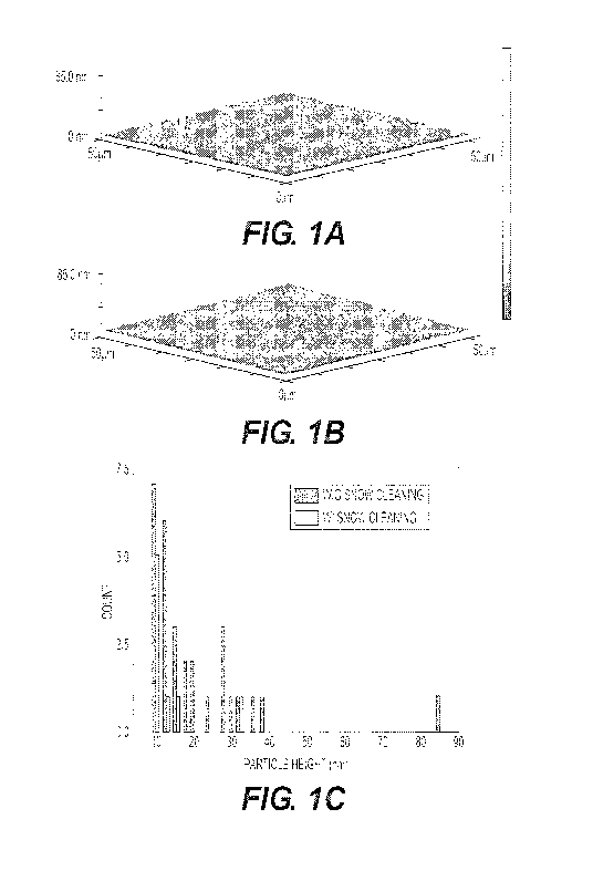
[017] Figure 1 depicts representative atomic force micrographs of the
surface of
indium tin oxide-coated glass substrates (a) before and (b) after CO2 snow
cleaning, and (c)
the statistics of particle heights on the two differently treated surfaces.
[018] Figure 2 depicts (a) series resistance (RSA) and fill factor (FF) for
SubPc
(open squares and dashed line), and DPSQ (solid squares and solid line) based
OPV cells
employing a C60 acceptor, (b) Short-circuit current (JO and power conversion
efficiency (lip)
for SubPc and DPSQ OPV devices with different areas. The same line symbols are
used as in
(a).
[019] Figure 3 depicts dark current density-vs-voltage (J-V) curves for
ITO/Mo03(15 nm)/DPSQ(13 nm)/C60(40 nm)/BCP(8 nm)/A1 devices with various
active
areas.
[020] Figure 4 depicts calculated dark J-V curves assuming RsA=50 n=cm2 and
variable R. Inset: calculated relationship between FF and shunt resistance.
[021] Figure 5 depicts J-V curves in dark and under 1 sun, AM 1.5G
illumination
for 6.25 cm2 devices showing the effects of the subelectrode.
[022] Figure 6 depicts current density vs voltage curves under 1 sun, AM 1.5G
illumination for three devices: A, B and C represented by a square, circle and
triangle in the
legend, respectively.
A: (control device): ITO/Mo03(10nm)/SubPc(13nm)/C60(40nm)/BCP(8 nm)/A1
B: ITO/PEDOT:PSS(50nm)/Mo03(5nm)/SubPc(13nm)/C60(40nm)/BCP(8 nm)/A1
C: ITO/Mo03(30nm)/SubPc(13nm)/C60(40nm)/BCP(8 nm)/A1
CA 02877904 2014-12-24
WO 2014/004364
PCT/US2013/047287
[023] Figure 7 depicts current density vs voltage curves under 1 sun, AM 1.5G
illumination for devices having a structure of
ITO/Mo03(10nm)/SubPc(13nm)/C60(40nm)/BCP(8 nm)/A1 with various active areas
and
with snow-plus-solvent cleaned substrates.
[024] Figure 8 depicts current density vs voltage curves under 1 sun, AM
1.5G
illumination for devices having a structure of
ITO/Mo03(10nm)/SubPc(13nm)/C60(40nm)/BCP(8 nm)/A1 with various active areas
and
with only snow-cleaned substrates.
[025] Figure 9 is an illustration of a snow cleaning apparatus, including a
CO2
source, a nozzle and a sample holder.
[026] As used herein, the term "layer" refers to a member or component of a
photosensitive device whose primary dimension is X-Y, i.e., along its length
and width, and
is typically perpendicular to the plane of incidence of the illumination. It
should be
understood that the term "layer" is not necessarily limited to single layers
or sheets of
materials. A layer can comprise laminates or combinations of several sheets of
materials. In
addition, it should be understood that the surfaces of certain layers,
including the interface(s)
of such layers with other material(s) or layers(s), may be imperfect, wherein
said surfaces
represent an interpenetrating, entangled or convoluted network with other
material(s) or
layer(s). Similarly, it should also be understood that a layer may be
discontinuous, such that
the continuity of said layer along the X-Y dimension may be disturbed or
otherwise
interrupted by other layer(s) or material(s).
[027] As used herein, the expression "disposed on" permits other materials
or
layers to exist between a disposed material and the material on which it is
disposed.
Likewise, the expression "deposited on" permits other materials or layers to
exist between a
deposited material and the material on which it is deposited. Thus, other
materials or layers
6
CA 02877904 2014-12-24
WO 2014/004364
PCT/US2013/047287
may exist between a surface of a substrate and a material "disposed on" or
"deposited on" the
surface of the substrate.
[028] As used herein, the term "yield" refers to the proportion of devices,
made or
manufactured by a process, that performs within a given range of
specifications.
[029] As described herein, exposing the surface of a substrate to a stream
of at least
one compound comprising one or more phases chosen from supercritical, gaseous,
solid, and
liquid phases permits the manufacture of large area solar devices having thin
organic layers,
e.g., a total deposited thickness of-7O nm, without compromising, and even
increasing,
yield. In some embodiments, the substrate is an ITO-coated substrate.
[030] In one embodiment, the present disclosure provides a multi-layer
solar
device comprising a substrate, and an active area comprising at least one
donor material and
at least one acceptor material deposited on a surface of the substrate,
wherein the donor and
acceptor materials are comprised of organic molecules, and wherein
particulates are removed
from the surface of the substrate before deposition of the donor and acceptor
materials. In
another embodiment, the present disclosure provides a multi-layer solar device
comprising a
pre-cleaned substrate having a surface substantially free of particulates, and
an active layer
comprising at least one donor material and at least one acceptor material
disposed on the
surface of the substrate, wherein the donor and acceptor materials are
comprised of organic
molecules.
[031] In some embodiments, the surface of the substrate comprises an
electrode,
such as an anode or cathode. In other embodiments, the multi-layer solar
device further
comprises an electrode deposited on the substrate, wherein particulates are
removed from the
surface of the substrate before deposition of the electrode.
[032] In another embodiment, a multi-layer solar device comprises a pre-
cleaned
substrate having a surface substantially free of particulates, two electrodes
in superposed
7
CA 02877904 2014-12-24
WO 2014/004364
PCT/US2013/047287
relation disposed on the surface of the pre-cleaned substrate, and an active
area comprising at
least one donor material and at least one acceptor material, wherein the donor
and acceptor
materials are comprised of organic molecules located between the two
electrodes.
[033] In some embodiments, the particulates are removed by exposing the
surface
of the substrate to a stream of at least one compound comprising one or more
phases chosen
from supercritical, gaseous, solid, and liquid phases. This process is
referred to herein as
"snow cleaning." In some embodiments, a substrate is pre-cleaned by snow
cleaning.
[034] In some embodiments, the stream of the at least one compound contains at
least gaseous and solid phases. In certain embodiments, the stream of the at
least one
compound contains gaseous, solid, and liquid phases. In certain embodiments,
the stream of
the at least one compound comprises a supercritical fluid.
[035] In some embodiments, the at least one compound is chosen to be gaseous
at
room temperature and atmospheric pressure. In further embodiments, the at
least one
compound forms a liquid or solid upon cooling below room temperature.
[036] In some embodiments, the exposure to the stream of the at least one
compound is via directed flow. In certain embodiments, the at least one
compound used to
remove particulates is CO2. This process of CO2 based cleaning is referred to
as CO2 snow
cleaning, or CO2 cleaning. CO2 snow cleaning is nondestructive, nonabrasive,
residue-free,
and environmentally friendly.
[037] In some embodiments, a compound other than, or in addition to, CO2 is
selected and used in a manner as described herein. The molecule chosen could
be selected
based on solvation properties for a particular contaminate, or chosen to
create a stream
containing one or more phases chosen from gas, liquid, solid and supercritical
phases.
Examples of compounds may include ammonia, nitrous oxide, various hydrocarbons
such as
acetylene, propane, butane or other hydrocarbons, various chlorinated
hydrocarbons such as
8
CA 02877904 2014-12-24
WO 2014/004364
PCT/US2013/047287
chloroethanes, various fluorinated hydrocarbons such as fluoroethanes, or
mixtures thereof
Exemplary compounds include those that form a liquid or solid upon cooling
below room
temperature.
[038] In some embodiments, snow-cleaned substrates are prepared by exposing a
surface of the substrate to at least one compound, such as CO2, around its
triple point, i.e., in
various parts of the stream, gas, liquid, and solid phases are present.
[039] In general, snow cleaning relies on the expansion of a liquid or
gaseous
compound, e.g., CO2, as it emerges from an orifice. The resulting stream of
material, e.g, a
combination of at least solid and gaseous phases, physically remove
particulates by the
momentum of the impacting solid particles and/or by the momentum of the gas,
thereby
overcoming the adhesional force binding particulates to the surface. Other
residues on the
substrate can be removed by dissolution of contaminates into a liquid or
supercritical fluid.
[040] In some embodiments of the present disclosure, the active area of the
solar
device ranges from about 0.01 cm2 to about 1000 cm2, from about 0.1 cm2 to
about 100 cm2,
from about 0.5 cm2 to about 50 cm2, from about 1 cm2 to about 10 cm2, and from
about 2.56
cm2 to about 6.25 cm2. In yet another embodiment, the active area ranges from
about 0.1 cm2
to about 6.25 cm2.
[041] In some embodiments, the active area of the solar device is a large
area of at
least about 0.25 cm2, about 0.5 cm2, about 1 cm2, about 5 cm2, about 6.25 cm2,
about 10 cm2,
about 50 cm2, about 100 cm2, or about 1000 cm2.
[042] Removed particulates may vary in size. In some embodiments, particulates
that are removed range in diameter from about 5 nm to about 1000 nm, from
about 15 nm to
about 200 nm, from about 20 nm to about 100 nm, and from about 30 nm to about
60 nm.
9
CA 02877904 2014-12-24
WO 2014/004364
PCT/US2013/047287
[043] In some embodiments, the organic active layer has a thickness ranging
from
about 10 nm to about 400 nm, from about 15 nm to about 120 nm, from about 20
nm to about
100 nm, and from about 50 to about 80 nm.
[044] In some embodiments, devices are prepared using snow-cleaned substrates
without any additional cleaning techniques. In another embodiment, the surface
of the
substrate is cleaned using a technique in addition to snow cleaning. Non-
limiting examples
of such additional techniques include wiping with a dry or wetted clean wipe,
sonicating in
detergent-water mixtures, and soaking in solvents such as, for example,
trichloroethylene,
acetone, and isopropanol.
[045] In yet another embodiment, snow cleaning increases yield without
compromising efficiency. In some embodiments, snow cleaning reduces or
eliminates short
circuits in the solar device.
[046] An additional embodiment of the present disclosure is directed to a
process
for manufacturing a photovoltaic device comprising, providing a substrate,
cleaning a surface
of the substrate by exposing the surface to a stream of at least one compound
comprising one
or more phases chosen from supercritical, gaseous, solid, and liquid phases,
and depositing an
organic active layer on the surface of the substrate.
[047] In some embodiments, the surface of the substrate exposed to the stream
of
the at least one compound comprises an electrode, such as an anode or cathode.
In some
embodiments, the process for manufacturing a photovoltaic device further
comprises
depositing two electrodes in superposed relation on the cleaned surface of the
substrate,
wherein the organic active layer is deposited between the two electrodes.
[048] In another embodiment of the present disclosure, a process for
manufacturing
a photovoltaic device comprises, providing a first electrode layer, cleaning
the first electrode
layer by exposing the first electrode layer to a stream of at least one
compound comprising
CA 02877904 2014-12-24
WO 2014/004364
PCT/US2013/047287
one or more phases chosen from supercritical, gaseous, solid, and liquid
phases, providing a
second electrode, wherein an organic active layer is deposited between the
first electrode
layer and the second electrode layer.
[049] In yet another embodiment, the present disclosure provides a process
for
manufacturing a photovoltaic device comprising, providing a first electrode
layer, cleaning
the first electrode layer by exposing the first electrode layer to a stream of
at least one
compound comprising one or more phases chosen from supercritical, gaseous,
solid, and
liquid and combinations thereof, providing a second electrode layer,
depositing an organic
active layer between the first electrode layer and the second electrode layer,
wherein the
thickness of the organic active layer is such that it improves yield over a
yield obtained
without cleaning the first electrode layer with the stream of the at least one
compound.
[050] The organic active layer as used herein may comprise at least one donor
material and at least one acceptor material.
[051] In some embodiments, the stream of the at least one compound contains at
least gaseous and solid phases. In certain embodiments, the stream of the at
least one
compound contains gaseous, solid, and liquid phases. In certain embodiments,
the stream of
the at least one compound comprises a supercritical fluid.
[052] In some embodiments, the at least one compound is chosen to be gaseous
at
room temperature and atmospheric pressure. In further embodiments, the at
least one
compound forms a liquid or solid upon cooling below room temperature.
[053] In some embodiments, the exposure to the at least one compound is via
directed flow. In certain embodiments, the at least one compound is CO2.
[054] In some embodiments, a compound other than, or in addition to, CO2 is
selected and used in a manner as described herein. The molecule chosen could
be selected
based on solvation properties for a particular contaminate, or chosen to
create a stream
11
CA 02877904 2014-12-24
WO 2014/004364
PCT/US2013/047287
containing one or more phases chosen from gas, liquid, solid and supercritical
phases.
Examples of compounds may include ammonia, nitrous oxide, various hydrocarbons
such as
acetylene, propane, butane or other hydrocarbons, various chlorinated
hydrocarbons such as
chloroethanes, various fluorinated hydrocarbons such as fluoroethanes, or
mixtures thereof
Exemplary compounds include those that form a liquid or solid upon cooling
below room
temperature.
[055] In certain embodiments, the organic active layer has an area ranging
from
about 0.01 cm2 to about 1000 cm2, from about 0.1 cm2 to about 100 cm2, from
about 0.5 cm2
to about 50 cm2, from about 1 cm2 to about 10 cm2, and from about 2.56 cm2 to
about 6.25
cm2. In certain embodiments, the active area ranges from about 0.1 cm2 to
about 6.25 cm2.
[056] In some embodiments, the organic active layer has a large area of at
least
about 0.25 cm2, about 0.5 cm2, about 1 cm2, about 5 cm2, about 6.25 cm2, about
10 cm2,
about 50 cm2, about 100 cm2, or about 1000 cm2.
[057] In some embodiments, the organic active layer has a thickness ranging
from
about 10 nm to about 400 nm, from about 15 nm to about 120 nm, from about 20
nm to about
100 nm, and from about 50 to about 80 nm.
[058] Additional layers, e.g., buffer layers and smoothing layers, may be
deposited
between the two electrodes. In some embodiments, the thickness of the
deposited layers
(e.g., buffer layers, smoothing layers, and/or active layers) are chosen to
improve yield. In
some embodiments, increasing the thickness of the deposited layers (e.g.
buffer layers,
smoothing layers, and/or active layers) improves yield.
[059] In one embodiment, snow cleaning is performed before loading into a
chamber, such as in the room ambient. In another embodiment, snow cleaning is
performed
in a load lock of a deposition tool, wherein the load lock is a chamber that
holds a substrate.
In some embodiments, the chamber is pumped down, a valve is opened to the
chamber, and a
12
CA 02877904 2014-12-24
WO 2014/004364
PCT/US2013/047287
substrate is transferred into the chamber. This allows samples to be loaded
into the
deposition chamber without exposing the chamber to ambient or atmospheric
pressure gases.
[060] In yet another embodiment, snow cleaning is performed in a deposition
chamber.
[061] In one embodiment, the present disclosure relates to an active area
within a
solar device comprising one or more materials that include a variety of
conjugated organic
molecules, such as, but not limited to phthalocyanines, functionalized
squaraines,
functionalized polyacenes, oligothiophenes, merocyanine dyes, modified
perylenes (e.g. DIP
or DBP) , conducting polymers, low-bandgap polymers, etc. as donor materials,
and acceptor
materials such as, but not limited to, the fullerenes, C60 or C70, or modified
polyacenes such
as NTCDA, PTCDA, PTCBI, PTCDI, etc.
[062] In some embodiments, the organic active layers are deposited on a
substrate,
for example, a piece of glass, metal or polymer. For solar cells, for example,
the substrate
may be transparent, such as glass. In some embodiments, the substrate
comprises an
electrode. In particular, the surface of the substrate exposed to the stream
of the at least one
compound may comprise the electrode. The electrode may be applied to serve as
a
conducting contact to the organic active layers. In some embodiments, the
conducting
electrode layer comprises an oxide, such as, indium/tin oxide (ITO).
[063] In another embodiment, OPV devices are made by sandwiching organic
layers between two metallic conductors, typically a layer of ITO with high
work function and
a layer of low work function metal such as Al, Mg or Ag.
[064] In some embodiments, the substrate surface is cleaned and
particulates are
removed before depositing layers on the substrate.
[065] In another embodiment, increasing the thickness of deposited layers
can at
least partially mitigate yield loss. Thickness can be increased by using a
buffer layer, e.g.,
13
CA 02877904 2014-12-24
WO 2014/004364
PCT/US2013/047287
poly (3,4-ethylenedioxythiophene):poly (styrenesulfonate) (PEDOT:PSS) or a
thick, e.g., 250
nm, polymer bulk heteroj unction active layer or a thicker than normal (t=103
nm) organic
layer, e.g., pentacene/C60/BCP. In yet another embodiment, a thick, Mo03 layer
can be
deposited on a substrate surface, such as an ITO surface.
[066] In some embodiments, solar cells fabricated and cleaned according to
the
methods of the present disclosure have a reduced occurrence of electrical
shorts.
Additionally, in some embodiments, a subelectrode structure may be used to
reduce device
resistance.
[067] In some embodiments, OPV devices may be fabricated using one or more
substrate cleaning procedures, e.g., solvent cleaning, in addition to snow
cleaning. Snow
cleaning, in particular CO2 snow cleaning, was found to be more effective than
conventional
solvent cleaning in reducing the density of defects that lead to shorts and
variations in device
performance, especially large-area devices.
EXAMPLES
[068] The present disclosure will now be described in greater detail by the
following non-limiting examples. It is understood that the skilled artisan
will envision
additional embodiments consistent with the disclosure provided herein.
Example 1
[069] Preparing substrates without snow cleaning: SubPc/C60 devices with
areas
A>0.64 cm2 have low yield due to shorts caused by particulates. To improve
yield, a thick
buffer layer (PEDOT:PSS or Mo03) prior to active layer deposition was
employed. The
device structures were ITO/Buffer layer(s)/SubPc(13 nm)/C60(40 nm)/BCP(8
nm)/Al.
Materials were deposited on ITO-coated glass substrates, with an ITO thickness
of ¨100 nm
and a sheet resistance of 20 5 n/sq. Mo03, boron subphthalocyanine chloride
(SubPc), C60/
and bathocuproine (BCP) were sequentially thermally evaporated at rates of
0.05, 0.1, 0.1,
14
CA 02877904 2014-12-24
WO 2014/004364
PCT/US2013/047287
and 0.05 nm/s, respectively, followed by a 100 nm thick Al cathode deposited
at 0.1 nm/s
through a shadow mask. All deposition rates and thicknesses were measured
using a quartz
crystal monitor and calibrated by variable angle spectroscopic ellipsometry.
Mo03 (Acros,
99.999%) and BCP (Lumtec, 99.5%) were used as received, and SubPc (Lumtec,
99%) and
C60 (MER, 99.9%) were further purified in a single cycle by thermal gradient
sublimation. In
one example, PEDOT:PSS (H.G. Stark, Clevios PH 500) was spun-coated, while
Mo03 was
thermally evaporated in vacuum.
[070] The fabricated device structures were as follows:
Device A (control): ITO/Mo03(10nm)/SubPc(13nm)/C60(40nm)/BCP(8 nm)/A1);
Device B: ITO/PEDOT:PSS(50nm)/Mo03(5nm)/SubPc(13nm)/C60(40nm)/BCP(8 nm)/A1,
Device C: ITO/Mo03(30nm)/SubPc(13nm)/C60(40nm)/BCP(8 nm)/Al.
[071] As shown in Table 1 and Figure 6, the increase of deposited layer
thickness
can degrade device performance. For the small area device (0.00785 cm2), the
power
conversion efficiency of the control structure (Device A: Mo03(10 nm)) was
qp=2.69 0.03%,
decreasing to 2.47 0.08% for devices with a PEDOT:PSS smoothing layer (Device
B:
PEDOT:PSS(50 nm)/Mo03(5 nm)), and 2.32 0.02% for devices with a relatively
thick Mo03
layer (Device C: Mo03(30 nm)). The decrease in efficiency for Devices B and C
as compared
to A arises primarily from a reduced fill factor. It is foreseeable that one
would want to both
snow clean and use a thicker buffer layer to minimize shorting as much as
possible.
[072] Fitting the dark J-V characteristics following the theory of Giebink,
as
described in C. Giebink, G.P. Wiederrecht, M.R. Wasielewski, and S.R. Forrest,
Phys. Rev. B
82, 155305 (2010), we found that the series resistance of Device C was RsA=5.4
0 .1 n=cm2
whereas RsA=0.77 0.02 n=cm2 for Device A. The increase in RA was due to the
increased
Mo03 layer thickness, which in turn led to a reduced FF and thus qp. Moreover,
Device B
CA 02877904 2014-12-24
WO 2014/004364
PCT/US2013/047287
had a larger dark saturation current density and smaller ideality factor that
also led to a
reduction in FF .
Table 1 The performance of representative SubPc/C60 devices.
Device 04) Avt
(gl.oa) OrlAicail)
A 0,62m101 2033 0.77-0,02 6'31-0,6 (11)A1e
B 0.5.6 0.01 247:E{8 1.2 0.1 =45 tt.t (1.3ze0.1)x104
C ()53+0,01 2.32O3 5 4+0.1 L;=.444),3 (1,W,1)Y1.0
Example 2
[073] An alternative to thicker buffer or active layers is to remove
particulates and
other asperities from the ITO surface using CO2 snow cleaning. Materials were
deposited on
ITO-coated glass substrates, with an ITO thickness of ¨100 nm and a sheet
resistance of 20 5
n/sq. Prior to film deposition, the ITO was cleaned as follows: first the
substrate was gently
wiped with a dry particle free wipe followed by 5 minute sonication in a
tergitol-deionized
water solution, 5 minute sonication in acetone, 10 minute soak in boiling
trichloroethylene,
minute sonication in acetone, and 10 minute immersion in boiling isopropanol.
Snow
cleaning was then performed for 90 seconds using an Applied Surface
Technologies (New
Providence, NJ, 07974) high-purity Model K4 snow cleaner. The substrates were
held at 50
C, with a nozzle angle of 45 with respect to the substrate, and a nozzle-to-
substrate distance
of ¨5 cm. The ITO was then exposed to ultraviolet-ozone for 10 minutes before
loading into a
high vacuum chamber (base pressure <2x10⁻⁷ Torr). Next, Mo03, boron
subphthalocyanine
chloride (SubPc), C60, and bathocuproine (BCP) were sequentially thermally
sublimed at
rates of 0.05, 0.1, 0.1, and 0.05 nm/s, respectively, followed by a 100 nm
thick Al cathode
deposited at 0.1 nm/s through a shadow mask. All deposition rates and
thicknesses were
measured using a quartz crystal monitor and calibrated by variable angle
spectroscopic
16
CA 02877904 2014-12-24
WO 2014/004364
PCT/US2013/047287
ellipsometry. Mo03 (Acros, 99.999%) and BCP (Lumtec, 99.5%) were used as
received, and
SubPc (Lumtec, 99%) and C60 (MER, 99.9%) were further purified in a single
cycle by
thermal gradient sublimation.
[074] Current density-vs.-voltage (J-V) characteristics in the dark and
under
simulated, 1 sun AM 1.5G solar illumination from a filtered Xe lamp were
measured in a
high-purity N2 filled glovebox. Optical intensities were referenced using an
NREL-calibrated
Si detector, and photocurrent measurements were corrected for spectral
mismatch. Errors
quoted correspond to the standard deviation for a device population of three
or more.
[075] Atomic force microscope (AFM) images in Figure 1(a) show large particles
distributed on the surface prior to snow cleaning, while Figure 1(b) shows
that the largest
particulates in the population had been completely removed by the cleaning
process. The
root-mean-square roughness for the ITO substrates decreased from 1.76 nm to
1.21 nm, but
more importantly, the peak-to-valley roughness decreased from 84.2 nm to 32.4
nm. The
largest of the particulates is most likely to short the devices as they were
larger than the total
organic layer thickness, and often were thicker than the entire active organic
layer region.
The particle size count statistics in Figure 1(c) show that snow cleaning had
removed most
median-sized, and all large particles.
[076] Large-area, snow-cleaned devices with thin organic layers (i.e.
torgz75 nm)
were also fabricated. Thermally evaporated and solution-processed devices with
structures of
ITO/Mo03(10 nm)/SubPc(13 nm)/C60(40 nm)/BCP(8 nm)/A1 (Device D) and
ITO/Mo03(15
nm)/DPSQ(13 nm)/C60(40 nm)/BCP(8 nm)/A1 (Device E), respectively, were
prepared with
active areas from 0.01 to 6.25 cm2. The partially solution-processed DPSQ/C60
devices were
fabricated where the DPSQ was spin coated on the Mo03 surface from 1.6 mg/ml
chloroform
solution at a rate of 3000 rpm for 30 seconds.
17
CA 02877904 2014-12-24
WO 2014/004364
PCT/US2013/047287
[077] As the area increases, no significant changes were observed in the
open-
circuit voltage (Voc), although the FF decreased for both Devices D and E as
shown in
Figure 2. The decrease in FF was due to the increase in series resistance from
Rsk---'1 n=cm2
for device with A=0.01 cm2, to Rsk---'180 n=cm2 for the device with A=6.25
cm2, resulting in
a concomitant decrease in short-circuit current (Jsc). From Figure 2, it is
apparent that the
series resistance needed to be RsA<lo n.cm2 to maintain the small-area device
performance
with increasing device size.
[078] In addition to the increase in RSA, larger area devices can also
exhibit high
dark current. In Figure 3, the dark J-V characteristics for DPSQ/C60 cells
with different areas
were fitted using the analysis of Giebink described in C. Giebink, G.P.
Wiederrecht, M.R.
Wasielewski, and S.R. Forrest, Phys. Rev. B 82, 155305 (2010). The results
showed that the
dark current due to leakage originating from the C60 acceptor layer had an
area-independent
saturation current density 0fJsA=(5.7 1.7)x10-11 mA/cm2 and a corresponding
ideality factor
of nA=1.50 0.01. However, the leakage dark current at low bias (e.g. less than
0.4 V) and
often associated with the donor, Jsp, increased by approximately 3 decades,
from
(1.0+0.3)x10-7 mA/cm2 to (0.9 0.1)x10-4 mA/cm2 as area increased from 0.01 cm2
to 6.25
cm2, an approximately linear correspondence. The increased dark current
indicated an
increased leakage across the donor due to shunt paths induced by particulates
not removed by
snow cleaning. Hence, it was the donor, deposited directly on the ITO surface,
whose leakage
was most directly affected by particles on the surface, leading to the
observed area
dependence ofJsp.
[079] In addition to an increase in dark current and series resistance, we
also found
that FF is reduced by shunt paths. This can be understood by including RA in
the excitonic
semiconductor ideal diode equation of Giebink, viz:
18
CA 02877904 2014-12-24
WO 2014/004364
PCT/US2013/047287
- r
4-
V ¨J=RsA +V¨ ___ SJ=R A
J = J , exp _________________________ T in
*-/ ph(
r ,=
nk BT I q i RA
(1)
[080] For simplicity, we can consider the case of a symmetric diode, with
identical
transport properties and injection barriers for both electrons and holes.
Here, Js and n are the
symmetric device saturation current and ideality factor, respectively, Jph is
the photocurrent
density, kB is the Boltzmann constant, T is the temperature, and q is
electronic charge. Finally,
is the polaron-pair dissociation rate relative to its equilibrium value.
[081] Figure 4 (inset) shows the dependence of FF on RA, where Jsc = Jph = 4.5
mA/cm2, J,= lx i0 mA/cm2, n = 2, ç = 1 and Rs = 0. The simulation showed that
FF
decreased with Rp, and was significantly reduced for RA < 2 kn=cm2. We also
plotted the J-V
characteristics predicted by Eq. (1) for several values of RA in Figure 4,
where we assumed
RsA=50 cm2. There was a pronounced dependence of FF on RA which is reflected
in the
data in Figure 4. For example, when the shunt resistance was 103 n.cm2, FF was
reduced by
25% from its value when RA¨>co.
[082] Another factor that led to deterioration in large-area OPV performance
was
the increase of series resistance dominated by the lateral resistance in the
ITO layer. To
reduce the effect of Rs on large-area OPV cells, we used a subelectrode
structure for devices
D and E (Figure 5 inset). The subelectrode allowed the carriers to travel a
shorter distance
from their point of generation before being collected at the metal contact. As
shown in
Figure 5, under 1 sun, AM 1.5G illumination, the A=6.25 cm2 SubPc/C60 device
with no
subelectrode showed lip =1.26 0.05% with J3.55 0.04 mA/cm2, FF=0 .32 0.01, and
RsA=179 4 cm2. Cells with a single subelectrode had a decreased series
resistance of
RsA=78 2 n.cm2, resulting in Jsc=3.91 0.09 mA/cm2, FF=0.46 0.01, and qp=2.02
0.08%,
while four subelectrodes further decreased the resistance to RsA=56 3 n=cm2,
resulting in
Jsc=3.95 0.05 mA/cm2, FF=0 .50 0 .01, and qp=2.21 0.05%. This represented
nearly a
19
CA 02877904 2014-12-24
WO 2014/004364
PCT/US2013/047287
doubling of lip compared to the device lacking a subelectrode. Similarly, for
the DPSQ/C60
device, the structure with a single subelectrode reduced RSA from 152 4 n.cm2
to 96 1
n=cm2, leading to a corresponding increase of Jsc from 4.47 mA/cm2 to 4.76
mA/cm2, FF
from 0.29 to 0.40, and lip from 1.21% to 1.78%.
Example 3
[083] Yields were investigated by fabricating a population of 1.44 cm2
devices.
The statistics of nineteen 1.44 cm2 out of twenty-seven total devices with
snow-plus-solvent
cleaned substrates, and sixteen 1.44 cm2 out of twenty-six devices with snow-
cleaned-only
substrates (without conventional solvent cleaning) were compared in Table 2.
Table 2 Parameters of OPVs with area of 1.44 cm2 with and without solvent
cleaning.
The standard deviation from the mean is SD.
Cleaning Jsc
Voc(V) FF r/P (%)
Process (mA/cm2)
Mean 1.09 4.13 0.56 2.52
Snow-plus-
solvent SD/Mean 0.4% 1.1% 3.8% 4.0%
Mean 1.10 3.83 0.50 2.10
Snow only
SD/Mean 1.3% 1.3% 2.7% 3.1%
[084] Using only CO2 snow cleaning, comparable yield of both small and large-
area devices were obtained (Figure 8). In contrast, using only solvent
cleaning, all devices
with area >0.64 cm2 were shorted. Using PEDOT:PSS (Device B) and thicker Mo03
(Device
C) coatings on the ITO, the yields of 2.56 cm2 devices were 50% and 67%,
respectively.
However, the thinner devices using snow-cleaned substrates had a higher yield
(-70%). This
indicates that CO2 snow cleaning is considerably more effective in reducing
surface
contaminants than using either thick buffer layers or solvent cleaning alone.
For both snow-
plus-solvent cleaned (Figure 7), and snow-cleaned-only substrates, the
standard deviations of
Voc and Jsc from their mean values were ¨1%. The standard deviation in fill
factor was
CA 02877904 2014-12-24
WO 2014/004364
PCT/US2013/047287
¨4.0% and was responsible for most of the variation in device efficiency. The
spread in FF
was caused by variations in dark current that arise from increased probability
of encountering
small particles in large-area devices, and variations in RSA (from 41 n.cm2 to
69 n.cm2) due
to variations encountered while probing devices.
[085] Snow cleaning of ITO-coated glass substrates is effective in the
removal of
contaminant particles, hence improving the yield of large-area OPV cells.
Using snow
cleaning, large-area devices exhibited a standard deviation of efficiency of
<4.0% from the
average. Further, the decrease of shunt resistance and increase of dark
current due to
particulates is evident when only conventional solvent substrate cleaning was
employed. The
existence of large particulates further resulted in the degradation of large-
area device
efficiency, fill factor, and yield. The relationship between FF and dark
current was shown to
be sensitive to the existence of shunt paths (and hence RA) caused by large
particles.
Furthermore, subelectrodes can reduce the series resistance, leading to a
power efficiency of
2.21 0.05% of SubPc/C60 device with an area of 6.25 cm2; or approximately 82%
that of an
analogous device with an area of only 0.00785 cm2.
21