Note : Les descriptions sont présentées dans la langue officielle dans laquelle elles ont été soumises.
CA 02879292 2015-01-21
METHOD AND APPARATUS FOR REPAIRING COMPOSITE MATERIALS
Field
This disclosure relates to composite materials, and more specifically to
apparatuses and methods for heating a bond portion of a composite material.
Background
Composite materials are typically made from two or more constituent materials
with significantly different physical or chemical properties. Typically, the
constituent
materials include a matrix (or bond) material, such as resin (e.g., thermoset
epoxy), and
a reinforcement material, such as a plurality of fibers (e.g., a woven layer
of carbon
fibers). When combined, the constituent materials typically produce a
composite
material with characteristics different from the individual constituent
materials even
though the constituent materials generally remain separate and distinct within
the
finished structure of the composite material. Carbon-fiber-reinforced polymer
is an
example of such a composite material.
Composite materials may be preferred for many reasons. For example,
composite materials may be stronger and/or lighter than traditional materials.
As a
result, composite materials are generally used to construct various objects
such as
vehicles (e.g., airplanes, automobiles, boats, bicycles, and/or components
thereof), and
non-vehicle structures (e.g., buildings, bridges, swimming pool panels, shower
stalls,
bathtubs, storage tanks, and/or components thereof).
Occasionally, these composite materials may become damaged, in which case it
may be preferable to repair the damaged composite material rather than replace
it
entirely. Currently, composite repairs are performed with heat blankets that
locally (or
in-situ) cure matrix material onto the existing damaged composite. However,
there are
various problems associated with using heat blankets, such as uneven heating,
misplaced heating, slow heating speeds, long cure times, thermal runaways,
and/or a
lack of adequate temperature control.
1
CA 02879292 2016-11-08
Summary
A method of bonding materials may comprise defining a bond interface between
two materials in a cure zone on a surface of an object, and non-conductively
heating the
bond interface without directly heating the surface outside of the cure zone.
Another method of bonding materials may comprise defining a bonding zone on
a surface of an object. The surface may include a deformity to be repaired. A
patch
material may be provided adjacent the deformity. A housing may be applied to
the
bonding zone. The housing may have at least one microwave emitter on an inner
side.
The emitter may be directed toward the bonding zone. The housing may be
configured
to prevent microwave emitter radiation from reaching the surface outside of
the bonding
zone. Microwave radiation may be emitted to the bonding zone until the patch
is suitably
bonded to the object.
An apparatus for bonding material may comprise a housing and one or more
microwave emitters. The housing may have an inner side and an opening. The one
or
more microwave emitters may be on the inner side of the housing. The housing
may be
configured for mounting on a surface having a fault requiring repair. The
opening of the
housing may be adjacent the surface, and may surround the fault. The housing
and the
surface may form a substantially closed chamber.
The present disclosure provides various apparatuses, and methods of use
thereof. In some embodiments, an apparatus may include a heating device, a
spacing
mechanism, and a shielding mechanism. In some embodiments, the heating device
may be a non-conductive, non-convective heating device, such as one or more
microwave emitters. In some embodiments, the spacing and shielding mechanisms
may
be a housing to which the one or more microwave emitters may be coupled.
In one embodiment there is provided a method of bonding materials. The method
involves defining a bond interface, having a first shape, between two
materials in a cure
zone on a surface of an object and non-conductively heating the bond interface
without
directly heating the surface of the object outside of the cure zone. Non-
conductively
heating the bond interface includes emitting microwave radiation from multiple
microwave emitters coupled to a housing having a second shape. The method
further
involves determining a temperature of the bond interface with a temperature
sensor,
2
modulating emission of the microwave radiation from at least a subset of the
microwave emitters based on the temperature of the bond interface, and
enclosing
the cure zone with the housing configured to isolate the cure zone from the
surface of
the object outside of the cure zone, and from a space surrounding the housing.
Enclosing the cure zone within the housing includes adjusting the second shape
of
the housing and sealing a flexible portion of the housing against a curved
portion of
the surface of the object.
In another embodiment there is provided a method of bonding materials. The
method involves defining a bonding zone on a surface of an object, the surface
including a deformity to be repaired. The method further involves providing a
patch
material adjacent the deformity and applying a housing to the bonding zone.
Multiple
microwave emitters are located on an inner side of the housing and are
directed
toward the bonding zone, the housing is configured to prevent microwave
radiation
from reaching the surface outside of the bonding zone, and the housing
includes a
first panel and a second panel, configured to move relative to the first
panel. The
method further involves emitting microwave radiation to the bonding zone until
the
patch is suitably bonded to the object. A bond interface between the object
and the
patch includes a first sub-interface and a second sub-interface non-coplanar
with
each other and the first panel is substantially parallel to the first sub-
interface and the
second panel is substantially parallel to the second sub-interface.
In another embodiment, there is provided an apparatus for bonding materials.
The apparatus includes a housing, having an inner side and an opening, and a
plurality of microwave emitters on the inner side of the housing. The housing
is
configured for mounting on a surface having a fault that requires repair. The
opening
of the housing is adjacent the surface and surrounds the fault. The housing
and the
surface form a substantially closed chamber. The housing includes at least a
first
panel and a second panel. The first panel includes a first microwave emitter
of the
plurality of microwave emitters, and the second panel includes a second
microwave
emitter of the plurality of microwave emitters. The apparatus further includes
a
reconfiguration device for altering an orientation of the first panel relative
to the
second panel, a controller for selectively powering the plurality of microwave
emitters,
2a
CA 2879292 2017-06-27
and one or more heat sensors, configured to measure a first temperature of a
first
location, proximate the fault, and to measure a second temperature of a second
location, proximate the fault, wherein the first location is spaced apart from
the
second location.
In another embodiment, there is provided an apparatus for bonding materials,
including a housing having an inner side and an opening, and a plurality of
microwave
emitters on the inner side of the housing. The housing is configured for
mounting on a
surface having a fault requiring repair, the housing including a flexible
portion
proximate the opening of the housing, the flexible portion configured to be
adjacent
the surface and to surround the fault so that the housing and the surface form
a
closed chamber. The apparatus further includes a temperature sensor configured
to
determine a temperature of the surface proximate the fault, and a controller
configured to modulate emission of microwave radiation from the plurality of
microwave emitters based on the temperature of the surface proximate the
fault.
In another embodiment, there is provided an apparatus for bonding materials,
including a housing, having an inner side and an opening, the housing
including a first
panel and a second panel. The apparatus further includes a plurality of
microwave
emitters on the inner side of the housing. The housing is configured for
mounting on a
surface having a fault requiring repair, the opening of the housing being
adjacent the
surface and surrounding the fault, the housing and the surface forming a
substantially
closed chamber, the fault including a first sub-interface and a second sub-
interface,
non-coplanar with each other. The first panel is adjustable to be
substantially parallel
to the first sub-interface and the second panel is adjustable to be
substantially parallel
to the second sub-interface.
The features, functions, and advantages may be achieved independently in
various embodiments of the present disclosure, or may be combined in yet other
embodiments, further details of which can be seen with reference to the
following
description and drawings.
Brief Description of the Drawings
Fig. 1 is a block diagram of an illustrative apparatus and an illustrative
object.
2b
CA 2879292 2017-06-27
CA 02879292 2015-01-21
Fig. 2 is an illustration of an airplane having a damaged external surface and
a
damaged internal surface.
Fig. 3A is a cross-sectional illustration of the external damaged surface of
Fig. 2.
Fig. 3B is a cross-sectional illustration of the external damaged surface
prepared
for repair with a patch.
Fig. 3C is a schematic illustration of an apparatus including a housing
coupled to
the external damaged surface to heat a bond interface between the patch and
the
external damaged surface.
Fig. 3D is a schematic illustration similar to Fig. 3C, but showing the bond
interface in a cured state.
Fig. 4A is a cross-sectional illustration of another damaged surface.
Fig. 4B is a cross-sectional illustration of the damaged surface of Fig. 4A
prepared for repair with a pair of opposing patches.
Fig. 4C is a schematic illustration of the apparatus of Fig. 3C in a
reconfigured
state, and a second apparatus similar to the apparatus of Fig. 3C, with the
apparatuses
coupled to the prepared damaged surface of Fig. 4B to heat respective bond
interfaces
between the patches and the prepared damaged surface.
Fig. 5 is a schematic illustration of an alternative set-up for heating the
respective
bond interfaces between the patches and the prepared damaged surface.
Fig. 6 is a schematic illustration of the two apparatuses of Fig. 3C
reconfigured to
optimize an emission profile to compliment a topography of the bond
interfaces.
Fig. 7 is a semi-schematic perspective illustration of the apparatus of Fig.
3C in
another reconfigured state, and showing temperature sensors and polarizing
mechanisms coupled to the housing.
Fig. 8 is a cross-sectional illustration of the apparatus of Fig. 7 taken
along the
line 8-8.
Fig. 9 is a chart of an illustrative bond cure cycle.
Fig. 10 is a flowchart illustrating a method for bonding materials, including
a non-
conductive heat ramp-up phase, a dwell phase, and a cool down phase.
Fig. 11 is an illustration of operations performed by one embodiment of a
feedback loop for the non-conductive heat ramp-up phase.
3
CA 02879292 2015-01-21
Fig. 12 is an illustration of operations performed by one embodiment of a
feedback loop for the dwell phase.
Fig. 13 is an illustration of operations performed by one embodiment of a
feedback loop for the cool down phase.
Fig. 14 is a flowchart illustrating another method for bonding materials.
Fig. 15 is a flowchart illustrating yet another method for bonding materials.
Fig. 16 is a schematic diagram of an illustrative data processing system.
Description
Overview
Various embodiments of apparatuses and methods for bonding materials are
described below and illustrated in the associated drawings. Unless otherwise
specified,
an apparatus or method and/or their various components or steps may, but are
not
required to, contain at least one of the structures, components,
functionality, and/or
variations described, illustrated, and/or incorporated herein. Furthermore,
the structures,
components, functionalities, and/or variations described, illustrated, and/or
incorporated
herein in connection with the apparatuses and methods may, but are not
required to, be
included in other similar apparatuses or methods. The following description of
various
embodiments is merely exemplary in nature and is in no way intended to limit
the
disclosure, its application or uses. Additionally, the advantages provided by
the
embodiments, as described below, are illustrative in nature and not all
embodiments
provide the same advantages or the same degree of advantages.
Specific Examples, Major Components, and Alternatives
Example 1:
This example describes an illustrative apparatus for bonding materials to an
object; see Fig. 1.
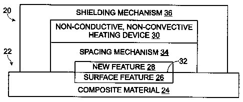
Fig. 1 is a schematic diagram of an apparatus, generally indicated at 20, and
an
object, generally indicated at 22. Object 22 may include a component made of a
composite material 24. Composite material 24 may have a surface feature 26.
4
CA 02879292 2015-01-21
Apparatus 20 may be coupled to composite material 24 to bond a new feature 28
to
surface feature 26. In some embodiments, surface feature 26 may be a fault in
composite material 24, in which case, new feature 28 may be a repair patch,
and
surface feature 26 may be prepared and/or altered before new feature 28 is
bonded to
composite material 24.
Apparatus 20 may include a non-conductive, non-convective heating device 30.
For example, heating device 30 may include one or more microwave emitters
(e.g., one
or more magnetrons). The one or more microwave emitters may be operable to
emit
microwave radiation to non-conductively and non-convectively heat a bond
interface 32
between new feature 28 and surface feature 26. Bond interface 32 may include a
bond
portion of a composite, such as a layer of thermo-curable (or thermo-setting)
matrix
material. Device 30 may suitably heat the bond portion to cure the bond
portion, and
thus bond new feature 28 to pre-existing composite material 24.
Apparatus 20 may include a spacing mechanism 34 to provide a suitable spacing
between device 30 and bond interface 32. For example, microwave radiation
emitted
from device 30 may have a wavelength A, in which case the suitable spacing
provided
by mechanism 34 may be at least A/4. The spacing provided by mechanism 34 may,
in
some embodiments, be less than A/4. However, microwave heating is generally
greatest
at odd multiples of A/4 (e.g., A/4, 3A14, 5A/4, etc.). Thus, if the provided
spacing is less
than one quarter of a wavelength (e.g., A/5), then heating bond interface 32
to a suitable
degree may involve operating device 30 for a longer period of time and/or
emitting
radiation having a greater amplitude.
In some embodiments, mechanism 34 may be disposed between device 30 and
bond interface 32. For example, mechanism 34 may be a layer of foam or plastic
that is
substantially microwave transparent. In other embodiments, mechanism 34 may be
disposed external to the provided spacing. For example, mechanism 34 may be a
frame
or housing to which device 30 may be connected or coupled.
Apparatus 20 may include a shielding mechanism 36. Shielding mechanism 36
may be configured to substantially contain all (or most) of the emitted
radiation between
shielding mechanism 36 and composite material 24. For example, shielding
mechanism
36 may be made of a material with a high loss factor, such as steel or
aluminum. In
5
CA 02879292 2016-11-08
some embodiments, shielding mechanism 36 may be a housing that provides the
spacing between device 30 and bond interface 32.
Example 2:
This example describes another illustrative apparatus for bonding materials to
an
object; see Figs. 2 ¨ 7.
Fig. 2 depicts an illustrative object 40. Object 40 may include one or more
components, such as fuselage skin, wing skin, a frame, a plurality of floor
beams,
and/or a plurality of horizontal stabilizers. The one or more components may
be made of
one or more composite materials, such as a laminate material, a honeycomb
material,
and/or one or more of the various exemplary composite materials described in
U.S.
Patent Nos. 8,490,348 and 8,642,168. While Fig. 2 shows object 40 to be an
airplane,
the object may be any other suitable structure, such as an automobile or a
building.
In some cases, it may be desirable to define a bonding (or cure) zone on a
portion of the object. For example, it may be desirable to define the bonding
zone in
order to add a new surface feature to an existing surface feature of one of
the
components of object 40. Examples of new surface features may include
additional
layers of reinforcement, and/or a new flange for mounting yet another feature.
In the
immediate example, it may be desirable to define a bonding zone 42 on an
external
surface 44 of object 40 in order to repair an existing surface feature, such
as a fault (or
deformity, or damaged area) 46. Alternatively or additionally, it may be
desirable to
define a bonding zone 48 on an internal surface 50 of object 40 to repair a
fault 52.
Fault 46 and/or fault 52 may be the result of an impact (e.g., from a
technician dropping
a tool on the surface, or a collision with another object), decompression
stress, or fire
damage, for example. In some cases, either of faults 46 or 52 may require
repair in
order for object 40 to be safely operated. In other cases, either of these
faults may be a
cosmetic fault that does not require repair, but may be a desirable repair
nonetheless.
Fig. 3A shows a cross-sectional view of fault 46 in surface 44 of the
composite
material, which is indicated here at 100. Material 100 may be a laminate
including
existing matrix material 104, such as a thermo-set adhesive or epoxy that has
already
6
CA 02879292 2015-01-21
been cured, and existing reinforcement material 108, such as a plurality of
woven
carbon fiber layers. In Fig. 3A, fault 46 is shown as an indentation (or
breach) in surface
44 that extends through multiple layers of reinforcement material 108. In
other
examples, the fault may extend through a lesser or greater portion of material
100. For
example, the fault may be a scratch in surface 44, or may be a hole extending
all the
way through the material (e.g., as in Fig. 4A).
Preparing fault 46 for repair may involve removing a portion of composite
material 100 (e.g., by sanding and/or grinding material 100 proximate fault
46). For
example, preparing fault 46 may involve tapering the damaged area, as is shown
in Fig.
3B. Preferably, edge portions of fault 46 may be tapered with a taper ratio of
about 30:1
(e.g., so that an orientation of the edge may deviate from an orientation of
surface 44 by
only about 1.5 degrees). Fault 46 may then be cleaned with an approved
solvent.
A patch (or patch material) 120 may be created by bonding together multiple
repair plies 124 of composite material. Plies 124 may include alternating
layers of matrix
and reinforcement material, or any other suitable combination of materials.
Patch 120 may be positioned adjacent fault 46. For example, a layer of
adhesive
film 128 may be disposed between first and second layers 132, 136 of
positioning
fabric. Film 128 may be a matrix material, such as a thermo-setting adhesive.
Layers
132, 136 may be sheets of reinforcement material. Film 128 and layers 132, 136
may
be positioned in fault 46, such that layer 136 contacts fault 46. Patch 120
may then be
positioned in fault 46 (e.g., such that patch 120 contacts layer 132) to
define a bond
interface 140 between patch 120 and composite material 100, as shown in Fig.
30. Film
128 may permeate layer 132 to contact patch 120, and may permeate layer 136 to
contact composite material 100.
An apparatus, generally indicated at 200 in Fig. 3C, may be used to non-
conductively heat bond interface 140. Apparatus 200 may heat bond interface
140
without directly heating surface 44 outside of bonding zone 42. Bonding zone
42 may
be defined by containment of an area on surface 44 by apparatus 200.
Apparatus 200 may include a housing 204, one or more microwave emitters 208,
and circuitry 212. Emitters 208 may be connected to housing 204. Housing 204
may be
configured to direct emitters 208 toward bonding zone 42. Circuitry 212 may be
used to
7
CA 02879292 2015-01-21
selectively power emitters 208. When powered, emitters 208 may emit microwave
radiation 216 toward bonding zone 42 to heat bond interface 140. Emitters 208
may
emit radiation 216 to bonding zone 42 (e.g., to bond interface 140) until
patch 120 is
suitably bonded to composite material 100 of the object, as shown in Fig. 3D.
Referring back to Fig. 3C, housing 204 may be configured to at least partially
enclose bonding zone (or repair area) 42 to substantially contain (all of)
radiation 216
inside housing 204. For example, housing 204 may be configured to enclose
bonding
zone 42 to isolate bonding zone 42 from surface 44 outside of bonding zone 42,
and/or
from a space surrounding the housing. Such isolation may prevent radiation 216
from
reaching surface 44 outside of bonding zone 42 and/or the space surrounding
housing
204 which may be occupied by a technician. For example, housing 204 may be
made of
a material with a high loss factor. Housing 204 may have an inner side, an
outer side,
and an opening. Emitters 208 may be on (or connected to) the inner side of
housing
204, as shown in Fig. 3C. Housing 204 may be configured to be mounted on (or
coupled to) surface 44, such that the opening of housing 204 is adjacent
surface 44 and
surrounds the fault, and/or such that housing 204 and surface 44 form a
substantially
closed chamber, as is also shown in Fig. 3C.
In one example, housing 204 may include one or more panels, such as side
panels 220, 224, and ceiling panels 228, 232. While multiple emitters 208 are
shown
connected to ceiling panels 228, 232, one or more emitters may alternatively
or
additionally be connected to side panels 220, 224. The one or more panels may
include
rigid and/or flexible portions. For example, ceiling panels 228, 232 may be
substantially
rigid. Side panels 220, 224 may include respective rigid portions 220a, 224a,
and/or
respective flexible portions 220b, 224b. Rigid portions 220a, 224a may be
proximate
ceiling panels 228, 232. Flexible portions 220b, 224b may be proximate the
opening of
housing 204, and may be configured to provide an adequate seal between
apparatus
200 and surface 44. The adequate seal may not be "air tight", but rather may
prevent
radiation 216 from escaping the closed chamber. For example, the adequate seal
may
have gaps, but these gaps may have a maximum dimension that is smaller than
the
wavelength of radiation 216. Flexible portions 220b, 224b may be made of a
wire mesh,
or other flexible material, which may be configured to flexibly engage
composite 100
8
CA 02879292 2015-01-21
(e.g., to provide the adequate seal). Holes in the wire mesh may be smaller
than the
wavelength of radiation 216.
Apparatus 200 may be configured to create a plurality of different volumes
and/or
shapes. For example, housing 204 may include one or more reconfiguration
devices,
such as hinges 236, 240, 244, operatively connected to the one or more panels.
The
one or more reconfiguration devices may allow the size and/or shape of housing
204 to
be reconfigured (or customized) to accommodate various sizes and/or geometries
or
topographies of various surfaces, surface features, bonding zones, and/or bond
interfaces. For example, hinge 236 may hingedly connect panel 220 and panel
228 to
allow for an angle between panels 220, 228 to be adjusted. Similarly, hinge
240 may
hingedly connect panel 228 and panel 232, and hinge 244 may hingedly connect
panel
232 and panel 224. Adjusting the angles (or relative orientations) between the
one or
more panels may adjust the size of the opening of housing 204, which may
result in a
smaller or larger area of surface 44 being exposed to radiation 216.
Additionally or
alternatively, adjusting the angles may adjust a spacing provided between
emitters 208
and bond interface 140, and/or an orientation of the one or more panels
relative to bond
interface 140 and/or to one or more of the other panels.
In some embodiments, housing 204 may additionally or alternatively include a
continuous substantially flexible sheet, which may include an outer layer of
high loss
factor material.
Emitters 208 may be (or may include) one or more magnetrons. Emitters 208
may be configured to emit radiation (or microwaves) having a frequency in a
range of
about 2 GHz to 16 GHz, which may be suitable for heating a bond portion of the
composite (e.g., the thermo-setting adhesive). Frequencies outside of this
range may
not be suitable, or may be less effective for suitably heating the bond
portion. For
example, frequencies significantly above 16 GHz may heat the bond portion too
quickly,
and frequencies significantly below 2 GHz may produce a heating profile with
undesirably large cold spots.
Generally, maximum microwave heating occurs at a separation distance from
emitters 208 corresponding to odd multiples of quarter wavelengths of the
emitted
radiation. Thus, apparatus 200 preferably provides a spacing of at least one
quarter
9
CA 02879292 2015-01-21
wavelength between emitters 208 and bond interface 140. Emitted radiation with
a
frequency of 2 GHz has a wavelength of about 14.99 cm, and emitted radiation
with a
frequency of 16 GHz has a wavelength of about 1.87 cm. Thus, a minimum
provided
spacing may be in a range of about 0.47 cm to 3.75 cm. In some embodiments,
depending on the composition of the bond portion, topography of the bond
interface,
and/or the spacing and sealing provided by the apparatus, frequencies lower
than 2
GHz and/or greater than 16 GHz may be suitable.
Circuitry 212 may include, at least one temperature sensor 248, a controller
(or
power controller) 252, and a power supply 256. Sensor 248 may be configured to
measure a temperature of one or more locations inside bonding zone 42. For
example,
sensor 248 may include a thermocouple or infrared detector configured to
measure an
exposed surface temperature of patch 120, an exposed surface temperature of
bond
interface 140, and/or an exposed surface of surface 44 inside the closed
chamber.
Measurements from sensor 248 may be used to tailor (and/or monitor) the amount
of
radiation applied to bond interface 140, and in some embodiments may be used
to
avoid thermal runaways. Controller 252 may be configured for selectively
powering
emitters 208. For example, controller 252 may be configured to modulate power
provided to emitters 208 from power supply 256 based on the temperature
measurements from sensor 248 to modulate a heating rate of bond interface 140.
Modulating the power provided to emitters 208 may include modulating a duty
cycle of
one or more of the emitters (e.g., modulating a frequency at which one or more
of
emitters 208 are turned off and on to modulate the heating rate), modulating
an
emission frequency of radiation 216 (e.g., modulating the frequency of
radiation 216 to
modulate the heating rate), and/or modulating an amplitude of radiation 216
(e.g.,
modulating the amplitude of radiation 216 to modulate the heating rate).
Circuitry 212 may include a data processing system (e.g., as depicted in Fig.
16)
which may implement one or more feedback loops (e.g., as depicted in Figs. 11-
13) to
modulate and/or monitor the heating rate at which bond interface 140 is
heated. In
some embodiments, controller 252 may be programmed to implement the one or
more
feedback loops.
CA 02879292 2015-01-21
In some embodiments, apparatus 200 may be computer controlled. For example,
the data processing system of circuitry 212 may be configured to allow a user
to define
a heating program. The heating program may include computer readable
instructions
corresponding to specific temperatures, for specific times, and/or for
specific subzones
within bonding zone 42 in order to accurately heat bond interface 140. The
heating
program may be defined based on a thermal survey of the object in the vicinity
of
bonding zone 42. In some embodiments, the data processing system may be
configured to allow the user to select a heating program from a plurality of
pre-defined
(or predetermined, or preprogrammed) heating programs, rather than manually
define
the heating program. In some embodiments, the data processing system may be
configured to allow the user to input a geometric dataset, such as a digital
computer
aided drafting (CAD) model. The geometric dataset may correspond to a portion
of the
object in the vicinity of bonding zone 42. Based on the geometric dataset, the
data
processing system may determine, select, and/or recommend a matching or
optimum
heating program.
Fig. 3D shows bond interface 140 after it has been suitably heated, which may
correspond to a cured state of bond interface 140, such that patch 120 is
sufficiently
bonded to composite material 100.
Circuitry 212 may be configured to determine when bond interface 140 has been
suitably heated. In response to a suitably heated determination, circuitry 212
may power
down emitters 208. Circuitry 212 may be configured to indicate the suitably
heated
determination to the user. Circuitry 212 may be configured to indicate to the
user that
the emitters have been powered down and are no longer emitting microwave
radiation.
In response to either one of these indications, the user may remove (and/or
uncouple)
housing 204 from surface 44, and inspect the repair. In some embodiments, the
user
may sand or otherwise remove any undesirable artifacts (e.g., any bumps
adjacent
patch 120 that are not flush with surface 44).
After apparatus 200 is removed from surface 44, apparatus 200 may be used
(and/or reconfigured) to repair another damaged area in a location remote from
bonding
zone 42, such as a surface feature 80 (see Fig. 4A), which may be any
composite
surface feature (or surface feature made of a composite material) anywhere on
or in
11
CA 02879292 2015-01-21
object 40, or other object, such as an automobile, boat, or building. Feature
80 is shown
in Fig. 4A to be a fault. However, in other examples, the surface feature may
not be a
fault, but rather a location on (or in) the object to which it is desirable to
heat (and/or
cure) a composite bond interface to add a new article of manufacture.
As shown in Fig. 4A, feature 80 may be a hole that extends through a wall
formed by a composite material 300 having a surface 302. Similar to material
100,
material 300 may include one or more layers of reinforcement material
laminated in
matrix material.
As shown in Fig. 4B, edges of fault 80 may be prepared in a manner similar to
fault 46 (see Fig. 3B). Patches 304, 308 may be created (and/or prepared) in a
manner
similar to patch 120 to repair fault 80. Patch 304 may be placed in fault 80
to define
bond interfaces 312, 316 between patch 304 and material 300. For example,
patch 304
may be placed in fault 80 with an adhesive film 320 and positioning fabric
layers 324,
328 between patch 304 and material 300. Similarly, patch 308 may be placed in
fault 80
to define bond interfaces 332, 336 between patch 308 and material 300. For
example,
an adhesive film 340 and positioning fabric layers 342, 346 may be sandwiched
between patch 308 and material 300 to define bond interface 332, and an
adhesive film
350 and positioning fabric layers 342, 346 may be sandwiched between patch 308
and
material 300 to define bond interface 336. A bond interface 354 may be defined
by
positioning fabric layers 324, 328, 342, 346 and adhesive film 320 sandwiched
between
patches 304, 308. When sandwiched together adhesive films 320, 340, 350 may
permeate through layers 324, 328, 342, and/or 346 to create a sufficient bond
interface.
In Fig. 4C, apparatus 200 and an apparatus 400 are coupled to opposite sides
of
material 300 to define a bonding zone, which is shown here as including
subzones
380a, 380b. Apparatuses 200, 400 may be coupled to material 300 with any
suitable
structure, mechanism, or device. For example, one or more fasteners such as
one or
more straps, adhesives, magnets, clamps, or other suitable structure may be
used to
couple either one of the apparatuses to material 300.
In Fig. 4C, apparatus 200 is shown in a reconfigured state, as compared to
apparatus 200 in Fig. 3C. In Fig. 4C, side panels 220, 224 have been pivoted
outward
(via hinge connections provided by respective hinges 236, 244) to widen the
opening of
12
CA 02879292 2015-01-21
housing 204. Such a selective size adjustment (in this case a widening) may
allow for
apparatus 200 to be used to heat various bond interfaces having different
widths. In
some embodiments, reconfiguring or adjusting the shape of housing 204 may
involve
adjusting an angle el between panels 228, 232, as shown in Fig. 7.
Referring back to Fig. 4C, apparatus 400 may be similar to apparatus 200 in
structure and function. For example, apparatus 400 may include a housing 404,
one or
more microwave emitters 408, and circuitry 412. Housing 404 may be similar to
housing
204. Emitters 408 may be similar to emitters 208. Circuitry 412 may be similar
to
circuitry 212. Circuitry 412 may include at least one temperature sensor 448
(e.g., which
may be similar to sensor 248), a controller 452 (e.g., which may be similar to
controller
252), and a power supply 456 (e.g., which may be similar to power supply 256).
Apparatuses 200, 400 may be operated to non-conductively heat bond interfaces
312, 316, 332, 336, 354 without directly heating surface 302 (or a surface of
material
300 opposite surface 302 to which apparatus 400 is coupled) outside of bonding
subzones 380a, 380b. For example, emitters 208, 408 may emit microwave
radiation to
bonding zones 380a, 380b until patches 304, 308 are suitably bonded to
material 300.
In some embodiments, circuitry 412 and circuitry 212 may be in communication
with
one another, which may improve feed back control of the apparatuses.
In Fig. 4C, housings 204, 404 have been configured to form a hexagonally
shaped configuration around the bonding interfaces. Such a configuration may
improve
reflection of the emitted radiation off of the sides of the housings, which
may more
evenly distribute the emitted radiation across the bonding interfaces and/or
reduce an
occurrence of cold spots along the bond interfaces. In some embodiments,
either of
housings 204, 404 may be configured to form a hexagonally shaped chamber with
the
surface to which the respective housing is coupled. For example, side panels
220, 224
may each include a reconfiguration device that allows these panels to angle
outward in
a region proximal ceiling panels 228, 232, and to angle inward in a region
proximal
surface 302.
Fig. 5 shows an alternative set-up for repairing material 300. In Fig. 5,
material
300 may be prepared and patches may be applied in a similar manner to Fig. 4B.
Apparatus 200 may be coupled to one side of material 300, and a tool 500 may
be
13
CA 02879292 2015-01-21
coupled to the other side of material 300 (e.g., opposite apparatus 200).
Apparatus 200
may be operated to heat at least one of the bond interfaces formed between at
least
one of the patches and material 300 (and/or a bond interface formed between
the
patches). Tool 500 may support the patch (or patch portion) that is distal
apparatus 200.
Tool 500 may be configured to prevent microwave radiation from apparatus 200
from
escaping the bonding zone opposite apparatus 200. In some embodiments, tool
500
may be used to prevent any microwave radiation from passing through material
100
(see Fig. 3C) opposite apparatus 200.
Heating the bond interfaces from a single side, as shown in Fig. 5, may be
sufficient to adequately cure the bond interface. However, in some
embodiments,
apparatus 200 may be subsequently coupled to the opposite side to complete the
curing
process. In some embodiments, tool 500 may again be coupled to material 300
opposite the apparatus when completing the curing process.
Fig. 6 shows apparatuses 200, 400 in reconfigured states to tailor (or
optimize)
an emission profile to compliment a topography of bond interfaces 312, 316,
332, 336,
354. In the immediate example, the reconfiguration devices may enable
additional
panels (or modules) to be added to the respective housings 204, 404, and/or
the
orientation of the panels to be adjusted such that the emitters are
substantially
equidistant from the bond interfaces, which may provide for a more even
application (or
distribution) of emitted radiation across a predefined geometric dataset
representative of
the bond interfaces. Such a substantially evenly distributed emission profile
may more
evenly heat the bond interfaces, which may reduce adjustments made by the
circuitry
regarding the emitted radiation.
In particular, hinge 236 may enable panels 220, 228 to be disconnected from
one
another. A panel 602, which may include one or more additional microwave
emitters,
may be connected between panels 220, 228. Hinge 236 may hingedly connect panel
602 to panel 220. A hinge 604 may hingedly connect panel 602 to panel 228.
Similarly, hinge 240 may enable panels 228, 232 to be disconnected from one
another. A panel 606, which may include one or more additional microwave
emitters,
may be connected between panels 228, 232. Hinge 240 may hingedly connect panel
606 to panel 232. A hinge 608 may hingedly connect panel 606 to panel 228.
14
CA 02879292 2015-01-21
Similarly, hinge 244 may enable panels 232, 224 to be disconnected from one
another. A panel 610, which may include one or more additional microwave
emitters,
may be connected between panels 232, 224. Hinge 244 may hingedly connect panel
610 to panel 224. A hinge 612 may hingedly connect panel 610 to panel 232.
The hinges may be formed from dovetailed portions of the respective panels, an
example of which can be seen in Fig. 7. However, apparatus 200 may include
other
structures or mechanisms that allow for shape reconfiguration and/or
modularity of
housing 204, such a mechanism that allows the panels to slide relative to one
another.
As shown in Fig. 6, reconfigured apparatus 200 (as compared to apparatus 200
in Fig. 4C) now includes panel 602 in an orientation substantially parallel to
a
substantially horizontal portion of interface 312, panel 228 in an orientation
substantially
parallel to an angled portion of interface 312, panel 606 in an orientation
substantially
parallel to interface 354, panel 232 in an orientation substantially parallel
to an angled
portion of interface 316, and panel 610 in an orientation substantially
parallel to a
substantially horizontal portion of interface 316.
Relative positions of the emitters on the panels may be adjustable. For
example,
the emitters may be slidingly engaged with the panels via a track system, or
other
suitable mechanism, such as one or more magnets. In some embodiments, one or
more
of the emitters may be removably coupled to one or more of the panels, which
may
allow for the relative position(s) and number of emitters on the respective
panels to be
tailored to a specific application.
As also shown in Fig. 6, apparatus 400 may be similarly reconfigured to
optimize
an emission profile to bond interfaces 332, 336, 354, as apparatus 200 is to
bond
interfaces 312, 316, 354.
Fig. 7 shows apparatus 200 in yet another reconfigured state. This
reconfigured
state, among other applications, may be suitable for repairing a hat stringer
700 on a
curved surface 704. Stringer 700 and surface 704 may be composite surfaces of
object
40 (see Fig. 2).
A patch 708 may be placed over (or adjacent) a fault 712 in stringer 700.
Fault
712 may be prepared for repair prior to placement of patch 708. The opening of
housing
CA 02879292 2015-01-21
204 may be placed adjacent surface 704 with the opening surrounding fault 712
to form
a substantially closed chamber, as is shown.
Housing 204 may include side panels 716, 718. Panels 716, 718 may be made of
a flexible metal wire mesh, or other suitable substantially flexible high loss
factor
material. Panels 716, 718 may be configured to flexibly engage surface 704
(and the
surface of stringer 700) to provide a sufficient seal to prevent microwave
radiation
emitted by emitters 208 from escaping the substantially closed chamber.
Panel 716 may be connected to panels 220, 224, 228, and/or 232. Panel 718
may be connected to panels 220, 224, 228, and/or 232. In some embodiments,
panels
716, 718 may be connected (or removably connected) to one or more of the
panels
prior to housing 204 being placed on surface 704. In some embodiments, panels
716,
718 may be connected (or removably connected) to one or more of the panels
after
housing 204 has been placed on surface 704. In some embodiments, panels 716,
718
may include stretchable portions that enable the shape of housing 204 to be
reconfigured without removal of panels 716, 718.
Lower portions of panels 220, 224 may include respective flexible portions
220b,
224b (see Fig. 3C) configured to provide a sufficient seal between surface 704
and
panels 220, 224. In other embodiments, the lower portions of panels 220, 224
may be
rigid but still provide a sufficient seal, as is shown in Fig. 7.
Apparatus 200 may include any suitable structure, mechanism, or device for
preventing emitted radiation from escaping the closed chamber. For example,
gaps
between panels (e.g., between dovetailed hinge portions of the respective
panels at
hinges 236, 240, 244) may be configured to prevent passage of emitted
microwave
radiation from the closed chamber to the space outside of housing 204. For
example,
the hinges may be structured such that the gaps between dovetailing portions
of the
panels are less than a single wavelength of the emitted radiation. In some
embodiments, housing 204 (e.g., all of housing 204 or portions thereof, such
as the
hinges) may be enclosed in wire mesh, or other suitable shielding mechanism
prior to or
after disposal on the surface.
In the reconfigured state of apparatus 200 shown in Fig. 7, angle 01 has been
adjusted to be less than angle 01 in the housing configuration shown in Fig.
4C, which
16
CA 02879292 2015-01-21
may provide for more evenly distributed heating along a convex bond interface
(e.g.,
between patch 708 and stringer 700). For example, by reducing angle 81 to a
suitable
angle that is less than 180 degrees, an array of emitters 208 coupled to panel
228 may
be positioned approximately equidistant from a first portion 708a of patch
708, and an
array of emitters 208 coupled to panel 232 may be positioned approximately
equidistant
from a second portion 708b of patch 708. The adjustment of angle 81 (e.g., via
operation of hinge 240) may result in an altered orientation of panel 228
relative to
panel 232.
Sensor (or sensor unit) 248 may be or include one or more temperature (or
heat)
sensors. The one or more temperature sensors may be configured to measure a
first
temperature of a first location proximate fault 712. For example, sensors 248
may
include a first infrared detector (or camera) 722, which may be configured to
measure a
temperature of the first location, which may be proximate first portion 708a
of patch 708.
Sensors 248 may be configured to measure a second temperature of a second
location proximate fault 712. For example, sensors 248 may include a second
infrared
detector (or camera) 726, which may be configured to measure a temperature of
the
second location, which may be proximate second portion 708b of patch 708. The
first
location may be spaced apart from the second location.
The one or more feedback loops, which may be implemented in circuitry 212,
may be configured to modulate emission of microwave radiation from the array
of
emitters 208 coupled to panel 228 (e.g., all or a subset of these emitters,
such as an
emitter 208a) based on the first temperature, and to modulate emission of
microwave
radiation from the array of emitters 208 coupled to panel 228 (e.g., all or a
subset of
these emitters, such as an emitter 208b) based on the second temperature.
In some embodiments, a single detector may be configured to measure
temperature in both the first and second locations. For example, the single
detector may
be a single infrared camera configured to acquire a thermal image of the
bonding zone
defined by housing 204 on the surface. Circuitry 212 may receive the acquired
thermal
image, and may associate distinct first and second regions in the image with
the
respective first and second locations. Circuitry 212 may modulate emissions
from the
array of emitters associated with panel 228 based on a temperature determined
from
17
CA 02879292 2015-01-21
the first region of the image, and/or may modulate emissions from the array of
emitters
associated with panel 232 based on a temperature determined from the second
region
of the image.
In some embodiments, circuitry 212 may be configured to activate different
emitters 208 sequentially. Circuitry 212 may be configured to tailor the
sequence and/or
intensity of emission to create stronger emitted radiation in one area of the
bonding
zone (e.g., proximal the first location) than in another area in the bonding
zone (e.g.,
proximal the second location).
Apparatus 200 may include any suitable mechanism, structure, or device for
altering a polarity (or directionality) of microwave emissions from one or
more of
emitters 208. For example, apparatus 200 may include one or more polarizing
mechanisms. Each polarizing mechanism may include a disc 730, as shown in
Figs. 7
and 8. Each disc may be rotatable relative to the panel to which it may be
coupled.
Each disc may include an elongate slot 734. Each disc 730 may be coupled to
one of
emitters 208, such that microwave radiation emitted by the respective emitter
is emitted
through the respective slot 734. Each of slots 734 may have a width that is
sufficiently
narrow to prevent passage of a first polarity of the emitted radiation, but
may have a
length that is sufficiently long to allow passage of a second polarity of the
emitted
radiation.
By rotating discs 730 (and thus slots 734), the emitted radiation may be
tailored
(and/or customized) to a particular application. For example, a particular
bond interface,
a particular housing configuration, and/or a particular emission frequency
combination
may result in one or more hot or cold spots in the bond interface produced by
additive
interference of the emitted radiation. To reduce such interference, one or
more of the
discs may be rotated to change the polarity of the emitted radiation. For
example,
adjacent slots 734a, 734b may be oriented relative to one another such that
their
respective elongate directions (or lengths) are substantially perpendicular to
one
another, as shown, such that the emitted radiation from slot 734a has a
polarity that is
substantially orthogonal to a polarity of radiation emitted from slot 734b,
which may
reduce interference at the bond interface due to a displacement variation from
emitters
208c, 208d to the bond interface.
18
CA 02879292 2015-01-21
Example 3:
This example describes an illustrative cure cycle (or process) for bonding
materials, which may be used in conjunction with any of the apparatuses
described
herein; see Fig. 9.
Fig. 9 shows a chart of an illustrative cure cycle, generally indicated at
900. Cycle
900 may include a heat ramp-up phase 904, a dwell phase 908, and a cool down
phase
912.
Prior to cycle 900, materials may be prepared to be bonded together at a bond
interface in a bonding zone, which may involve preparing a damaged area and/or
applying a patch. A vacuum bag, or other pressure reduction device, may be
applied to
the bonding zone to hold the materials together. An apparatus for bonding the
materials
may be used to define the bonding zone. In some embodiments, the vacuum bag
may
be placed over the apparatus (e.g., after the apparatus has defined the
bonding zone).
Phase 904 may begin at a first predetermined temperature (e.g., of a bond
interface defined between the materials), such as at 54 degrees Celsius. In
some
embodiments, emitted radiation from the apparatus of any of the foregoing
examples
may be used to heat the bond interface. In some embodiments, the materials
(and/or
the bond interface) may be initially heated by another source, such as a heat
gun, which
may be used to heat tack an adhesive layer and/or the materials in place.
Phase 904
may involve increasing the temperature of the bond interface at a first
predetermined
rate, such as at a rate in a range of about 0.5 to 3 degrees Celsius per
minute. Phase
904 may continue until the bond interface reaches a second predetermined
temperature, which may be a cure (or cured) temperature of the bond interface,
such as
a temperature of 177 degrees Celsius plus or minus 6 degrees Celsius.
Phase 908 may begin when the bond interface reaches the second
predetermined temperature. Phase 908 may involve holding or maintaining the
second
predetermined temperature for a predetermined duration of time, such as 150 to
210
minutes. Maintaining the second predetermined temperature for the
predetermined
duration of time may form a suitable bond between the materials (e.g., at the
bond
interface).
19
CA 02879292 2015-01-21
Phase 912 may start when the predetermined duration of time has lapsed. Phase
912 may involve decreasing the temperature of the bond interface at a second
predetermined rate, such as at a rate that is less than or equal to 3 degrees
Celsius per
minute. The second predetermined rate may be a maximum rate at which the
temperature of the bond interface can be reduced without reducing a strength
of the
bond. Phase 912 may continue until the bond interface reaches a third
predetermined
temperature, such as a temperature at or below 60 degrees Celsius. Once the
bond
interface has reached the third predetermined temperature, pressure inside the
vacuum
bag may be released, the vacuum bag and the apparatus may be removed, and the
bond between the materials may be inspected.
Example 4:
This example describes a method for bonding materials; see Figs. 10 - 13.
Fig. 10 depicts multiple steps of a method, generally indicated at 1000, which
may be performed in conjunction with an apparatus for bonding materials
according to
aspects of the present disclosure. Although various steps of method 1000 are
described
below and depicted in Fig. 10, the steps need not necessarily all be
performed, and in
some cases may be performed in a different order than the order shown.
Method 1000 may include a step 1002 of preparing a bonding zone. At step
1002, a surface feature of an object may be prepared to be bonded with a new
surface
feature. The surface feature may be a fault in the object, or may be a region
without a
fault. Preparing the surface feature may involve removing a portion of
material from the
object, applying the new surface feature to the (existing) surface feature of
the object,
and/or vacuum bagging and depressurizing a region in which the new surface
feature is
disposed to hold together the new surface feature and the surface feature of
the object.
At step 1002, an apparatus may be applied to the object to define the bonding
zone.
The apparatus may include a non-conductive, non-convective heating device,
such as
one or more microwave emitters, and a spacing mechanism and a shielding
mechanism, such as a housing made of a high loss material to which the heating
device
is coupled.
CA 02879292 2015-01-21
Method 1000 may include a step 1004 of performing a non-conductive heat
ramp-up phase, a step 1006 of performing a dwell phase, and a step 1008 of
performing
a cool down phase (e.g., similar to phases 904, 908, 912 shown in Fig. 9). At
step 1004,
the apparatus may be configured and/or operated to increase at a first rate a
temperature of a bond interface between the surface feature of the object and
the new
surface feature until the temperature of the bond interface reaches a first
predetermined
temperature (e.g., see phase 904 of Fig. 9). The first predetermined
temperature may
be a cured temperature of the bond interface. At step 1006, the apparatus may
be
configured and/or operated to maintain a temperature of the bond interface at
(or
around) the first predetermined temperature for a predetermined duration of
time (e.g.,
see phase 908 of Fig. 9). At step 1008, the apparatus may be configured and/or
operated to allow the temperature of the bond interface to decrease at a
second
predetermined rate until the bond interface reaches a second predetermined
temperature (e.g., see phase 912 of Fig. 9).
Method 1000 may include a step 1010 of inspecting a bond formed between the
material (e.g., the new surface feature and the surface feature of the
object). At step
1010, a user may remove the apparatus from the surface of the object, remove
the
vacuum bag, and inspect the bond to see if the apparatus has adequately heated
the
bond interface to provide a desirable cure.
Fig. 11 is an illustration of operations, generally indicated at 1100, which
may be
performed by one embodiment of a feedback loop for the non-conductive heat
ramp-up
phase. This feedback loop may be implemented in circuitry of the apparatus.
Operations 1100 may include a step 1102 of acquiring a surface temperature
reading. The surface temperature reading may include a measurement of the
surface
temperature of the surface feature of the object and/or the new surface
feature, which
may be proximate the bond interface. One or more temperature sensors of the
apparatus may acquire the surface temperature reading. A controller, or other
suitable
circuitry of the apparatus, may receive the surface temperature reading from
the one or
more temperature sensors.
Operations 1100 may include a step 1104 of converting the surface temperature
to an inner ply temperature. The one or more microwave emitters may non-
conductively
21
CA 02879292 2015-01-21
and non-convectively heat the bond interface via directed microwave radiation.
The
microwave radiation may directly excite molecular structures in a bond portion
(e.g., an
adhesive) of the bond interface, which may be in a non-exposed location. For
example,
bond interface 354 in Fig. 4C may correspond to a location of an inner ply of
the bond
interface that is non-exposed. Excitation of the molecular structures in this
non-exposed
location may produce heat which may be conductively transmitted to other
portions of
the bond interface. Heat conductively transmitted to exposed portions of the
bond
interface (e.g., the horizontal portion of bond interface 312 in Fig. 4C), may
be
convectively dissipated. However, heat conductively transmitted to other non-
exposed
portions of the bond interface (e.g., a lower segment of the angled portion of
bond
interface 312 in Fig. 4C) may not be convectively dissipated, which may result
in the
inner ply temperature being higher than the surface temperature. At step 1104,
the
circuitry of the apparatus (e.g., the controller, and/or a data processing
system) may
determine the inner ply temperature based on the measured surface temperature.
The
determined inner ply temperature may be an estimate, based on one or more
factors,
such as bond interface topography, a depth of the bond interface, and/or
compositions
of the materials being bonded. The circuitry may determine the inner ply
temperature by
accessing a conversion table. The conversion table may associate specific
surface
temperatures with specific predetermined inner ply temperatures.
Operations 1100 may include a step 1106 of determining whether the inner ply
temperature is equal to (or has reached) the cured temperature. In some
examples, the
cured temperature may be around 177 degrees Celsius. In other examples, the
cured
temperature may be around 121 degrees Celsius. At step 1106, the circuitry of
the
apparatus may determine whether the inner ply temperature is equal to (or has
reached) the cured temperature. If it is determined that the inner ply
temperature has
reached the cured temperature, then operations 1100 may flow to a step 1108 of
proceeding to the dwell phase (e.g., see phase 908 in Fig. 9, and step 1006 in
Fig. 10).
However, if it is determined at step 1106 that the inner ply temperature is
not
equal to (e.g., is less than) the cured temperature, then operations 1100 may
proceed to
a step 1110. At step 1110, the circuitry may determine whether an inner ply
temperature
rate increase is less than a first predetermined threshold rate, such as 0.5
degrees
22
CA 02879292 2015-01-21
Celsius per minute. If it is determined at step 1110 that the rate increase is
less than the
first predetermined threshold rate, then operations 1100 may proceed to a step
1112 of
increasing power to one or more of the microwave emitters, and may return to
step
1102. If it is determined at step 1110 that the rate increase is not less than
the first
predetermined threshold rate, then operations 1100 may proceed to a step 1114.
At step 1114, the circuitry may determine whether the inner ply temperature
rate
increase is greater than a second predetermined threshold rate, such as 3
degrees
Celsius per minute. If it is determined at step 1114 that the inner ply
temperature rate
increase is not greater than the second predetermined threshold rate, then
operations
1100 may return to step 1102. However, if it is determined at step 1114 that
the inner
ply temperature rate increase is greater than the second predetermined
threshold rate,
then operations 1100 may proceed to a step 1116 of decreasing power to one or
more
of the microwave emitters, and may return to step 1102.
Fig. 12 is an illustration of operations, generally indicated at 1200, which
may be
performed by one embodiment of a feedback loop for the dwell phase. This
feedback
loop may be implemented in the circuitry of the apparatus.
Operations 1200 may include a step 1202 of acquiring a surface temperature
reading, and a step 1204 of converting the acquired surface temperature to an
inner ply
temperature. Step 1202 may be similar to step 1102 of operations 1100. Step
1204 may
be similar to step 1104 of operations 1100.
Operations 1200 may include a step 1206 of determining whether the inner ply
temperature is less than a lower threshold temperature. The lower threshold
temperature may be the cured temperature (or a lower predetermined temperature
in a
range of temperatures at which the bond interface may be properly cured). If
it is
determined at step 1206 that the inner ply temperature is less than the lower
threshold
temperature, then operations 1200 may proceed to a step 1208 of increasing
power to
one or more of the microwave emitters, and may return to step 1202.
However, it is determined at step 1206 that the inner ply temperature is not
less
than the lower threshold temperature, then operations 1200 may proceed to a
step 1210
of determining whether an elapsed time in the dwell phase has reached (or is
equal to)
23
CA 02879292 2015-01-21
a predetermined duration of dwell time. The predetermined duration of dwell
time may
be a duration of dwell time that is required for the bond interface to be
properly cured.
If it is determined at step 1210 that the elapsed time has not reached the
predetermined duration, then operations 1200 may proceed to a step 1212 of
determining whether the inner ply temperature is greater than an upper
threshold
temperature. The upper threshold temperature may be an upper predetermined
temperature in a range of temperatures at which the bond interface may be
properly
cured. If it is determined at step 1212 that the inner ply temperature is
greater than the
upper threshold temperature, then operations 1200 may proceed to a step 1214
of
decreasing power to one or more of the microwave emitters, and return to step
1202.
However, if it is determined at step 1212 that the inner ply temperature is
not greater
than the upper threshold temperature, then operations may return to step 1202
(e.g.,
without decreasing power to one or more of the microwave emitters).
At step 1210, if it is determined that the elapsed time has reached the
predetermined duration, then operations 1200 may flow to a step 1216 of
proceeding to
the cool down phase (e.g., see phase 912 in Fig. 9, and step 1008 in Fig. 10).
Fig. 13 is an illustration of operations, generally indicated at 1300, which
may be
performed by one embodiment of a feedback loop for the cool down phase. This
feedback loop may be implemented in the circuitry of the apparatus.
Operations 1300 may include a step 1302 of acquiring a surface temperature
reading, and a step 1304 of converting the acquired surface temperature to an
inner ply
temperature. Step 1302 may be similar to step 1102 of operations 1100. Step
1304 may
be similar to step 1104 of operations 1100.
Operations 1300 may include a step 1306 of determining whether an inner ply
temperature rate decrease is less than a third predetermined threshold rate.
The third
predetermined threshold rate may be a rate at which the inner ply temperature
may
decrease without damaging the cured bond. For example, the third predetermined
threshold rate may be 3 degrees Celsius per minute. If it is determined at
step 1306 that
the inner ply temperature rate decrease is not less than the third
predetermined
threshold rate, then operations 1300 may proceed to a step 1308 of decreasing
power
to one or more of the microwave emitters, and may return to step 1302.
However, if it is
24
CA 02879292 2015-01-21
determined at step 1306 that the inner ply temperature decrease is not less
than the
third predetermined threshold rate, then operations 1300 may proceed to a step
1310 of
determining whether the inner ply temperature is less than or equal to a
suitably cool
temperature, such as 60 degrees Celsius. The suitably cool temperature may be
a
temperate at or below which the temperature of the cured bond interface can
decrease
at a rate greater than the third predetermined threshold rate without causing
damage to
the cured bond.
At step 1310, if it is determined that the inner ply temperature is not less
than or
equal to the suitably cool temperature, then operations 1300 may return to
step 1302.
However, if it is determined at step 1310 that the inner ply temperature is
less than or
equal to the suitably cool temperature, then operations 1300 may proceed to a
step
1312 of turning off power to the one or more microwave emitters.
Example 5:
This example describes another method for bonding materials; see Fig. 14.
Fig. 14 depicts multiple steps of a method, generally indicated at 1400, which
may be performed in conjunction with an apparatus for bonding materials
according to
aspects of the present disclosure. Although various steps of method 1400 are
described
below and depicted in Fig. 14, the steps need not necessarily all be
performed, and in
some cases may be performed in a different order than the order shown.
Method 1400 may include a step 1402 of defining a bond interface between two
materials in a cure zone on a surface of an object. A patch may be created by
bonding
together multiple plies of composite material. At step 1402, a surface feature
of the
object may be prepared to be bonded with the patch. Preparation of the surface
feature
may involve sanding, grinding, or otherwise removing some material from the
surface
feature. The surface feature may be associated with the surface and may be one
of the
two materials. The surface feature may include an indentation in the surface.
The
surface feature may include a hole through a wall. The patch may be the other
of the
two materials. Defining the bond interface may include applying a thermo-
setting
adhesive between the patch and the prepared surface feature.
CA 02879292 2015-01-21
Method 1400 may include a step 1404 of non-conductively heating the bond
interface without directly heating the surface outside of the cure zone. For
example, the
cure zone may be enclosed with a housing configured to isolate the cure zone
from the
surface of the object outside of the cure zone, and from the space surrounding
the
housing. Enclosing the cure zone may involve adjusting a shape of the housing,
and
sealing a flexible portion of the housing against a curved portion of the
surface of the
object. Heating the bond interface may involve applying microwave radiation to
the bond
interface. Applying the microwave radiation may involve emitting the microwave
radiation from multiple microwave emitters coupled to the housing.
Method 1400 may include a step 1406 of determining a temperature in a location
in the bond zone, and modifying a heating effect at the location in response
to the
determined temperature. For example, step 1406 may involve determining a
temperature of the bond interface with a temperature sensor, and modulating
emission
of microwave radiation from at least a subset of the microwave emitters based
on the
determined temperature.
Example 6:
This example describes another method for bonding materials; see Fig. 15.
Fig. 15 depicts multiple steps of a method, generally indicated at 1500, which
may be performed in conjunction with an apparatus for bonding materials
according to
aspects of the present disclosure. Although various steps of method 1500 are
described
below and depicted in Fig. 15, the steps need not necessarily all be
performed, and in
some cases may be performed in a different order than the order shown.
Method 1500 may include a step 1502 of defining a bonding zone on a surface of
an object. The surface may include a deformity to be repaired. The surface may
be the
surface of a pre-existing composite material. The pre-existing composite
material may
have been previously cured.
Method 1500 may include a step 1504 of providing a patch material adjacent the
deformity. The patch may include matrix material and/or reinforcement
material. The
patch material provided adjacent the deformity may be in a cured state, or may
be in a
non-cured state.
26
CA 02879292 2015-01-21
Method 1500 may include a step 1506 of applying a housing to the bonding
zone. The housing may include an inner side, and an opening to the inner side.
The
housing may include at least one microwave emitter on the inner side of the
housing.
The housing may be configured to prevent microwave emitter radiation from
reaching
the surface outside of the bonding zone. For example, the housing may be made
of a
high loss factor material. Applying the housing to the bonding zone may
involve
coupling (e.g., positioning) the opening adjacent the surface. Applying the
housing to
the bonding zone may involve directing the at least one microwave emitter
toward the
bonding zone.
Optionally, method 1500 may include a step 1508 of configuring a shape of the
housing to optimize an emissions profile. For example, multiple microwave
emitters may
be coupled to the housing, and a bond interface may be defined between the
deformity
and the patch material, in which case, configuring the shape of the housing
may involve
tailoring an arrangement and/or geometry of the emitters to substantially
match a
topography of the bond interface.
Method 1500 may include a step 1510 of emitting microwave radiation to the
bonding zone until the patch is suitably bonded to the object. Suitably
bonding the patch
to the object may involve emitting microwave radiation from the at least one
microwave
emitter to the bonding zone to perform a heat ramp-up phase, a dwell phase,
and a cool
down phase on the bond interface. In some embodiments, emitting microwave
radiation
to the bonding zone may include applying microwave radiation having a first
polarity to a
first location in the bonding zone, and applying microwave radiation having a
second
polarity to a second location in the bonding zone. The first polarity may be
different than
(e.g., substantially orthogonal to) the second polarity.
Example 7:
This example describes a data processing system 1600 in accordance with
aspects of the present disclosure. In this example, data processing system
1600 is an
illustrative data processing system for implementing one or more of the
operations
and/or functions in Figs. 1 - 15 and/or described in relation thereto; see
Fig. 16.
27
CA 02879292 2015-01-21
In this illustrative example, data processing system 1600 includes
communications framework 1602. Communications framework 1602 provides
communications between processor unit 1604, memory 1606, persistent storage
1608,
communications unit 1610, input/output (I/O) unit 1612, and display 1614.
Memory
1606, persistent storage 1608, communications unit 1610, input/output (I/O)
unit 1612,
and display 1614 are examples of resources accessible by processor unit 1604
via
communications framework 1602.
Processor unit 1604 serves to run instructions for software that may be loaded
into memory 1606. Processor unit 1604 may be a number of processors, a multi-
processor core, or some other type of processor, depending on the particular
implementation. Further, processor unit 1604 may be implemented using a number
of
heterogeneous processor systems in which a main processor is present with
secondary
processors on a single chip. As another illustrative example, processor unit
1604 may
be a symmetric multi-processor system containing multiple processors of the
same
type.
Memory 1606 and persistent storage 1608 are examples of storage devices
1616. A storage device is any piece of hardware that is capable of storing
information,
such as, for example, without limitation, data, program code in functional
form, and
other suitable information either on a temporary basis or a permanent basis.
Storage devices 1616 also may be referred to as computer readable storage
devices in these examples. Memory 1606, in these examples, may be, for
example, a
random access memory or any other suitable volatile or non-volatile storage
device.
Persistent storage 1608 may take various forms, depending on the particular
implementation.
For example, persistent storage 1608 may contain one or more components or
devices. For example, persistent storage 1608 may be a hard drive, a flash
memory, a
rewritable optical disk, a rewritable magnetic tape, or some combination of
the above.
The media used by persistent storage 1608 also may be removable. For example,
a
removable hard drive may be used for persistent storage 1608.
Communications unit 1610, in these examples, provides for communications with
other data processing systems or devices. In these examples, communications
unit
28
CA 02879292 2015-01-21
1610 is a network interface card. Communications unit 1610 may provide
communications through the use of either or both physical and wireless
communications
links.
Input/output (I/O) unit 1612 allows for input and output of data with other
devices
that may be connected to data processing system 1600. For example,
input/output (I/O)
unit 1612 may provide a connection for user input through a keyboard, a mouse,
and/or
some other suitable input device. Further, input/output (I/O) unit 1612 may
send output
to a printer. Display 1614 provides a mechanism to display information to a
user.
Instructions for the operating system, applications, and/or programs may be
located in storage devices 1616, which are in communication with processor
unit 1604
through communications framework 1602. In these illustrative examples, the
instructions are in a functional form on persistent storage 1608. These
instructions may
be loaded into memory 1606 for execution by processor unit 1604. The processes
of the
different embodiments may be performed by processor unit 1604 using computer-
implemented instructions, which may be located in a memory, such as memory
1606.
These instructions are referred to as program instructions, program code,
computer usable program code, or computer readable program code that may be
read
and executed by a processor in processor unit 1604. The program code in the
different
embodiments may be embodied on different physical or computer readable storage
media, such as memory 1606 or persistent storage 1608.
Program code 1618 is located in a functional form on computer readable media
1620 that is selectively removable and may be loaded onto or transferred to
data
processing system 1600 for execution by processor unit 1604. Program code 1618
and
computer readable media 1620 form computer program product 1622 in these
examples. In one example, computer readable media 1620 may be computer
readable
storage media 1624 or computer readable signal media 1626.
Computer readable storage media 1624 may include, for example, an optical or
magnetic disk that is inserted or placed into a drive or other device that is
part of
persistent storage 1608 for transfer onto a storage device, such as a hard
drive, that is
part of persistent storage 1608. Computer readable storage media 1624 also may
take
the form of a persistent storage, such as a hard drive, a thumb drive, or a
flash memory,
29
CA 02879292 2015-01-21
that is connected to data processing system 1600. In some instances, computer
readable storage media 1624 may not be removable from data processing system
1600.
In these examples, computer readable storage media 1624 is a physical or
tangible storage device used to store program code 1618 rather than a medium
that
propagates or transmits program code 1618. Computer readable storage media
1624 is
also referred to as a computer readable tangible storage device or a computer
readable
physical storage device. In other words, computer readable storage media 1624
is a
media that can be touched by a person.
Alternatively, program code 1618 may be transferred to data processing system
1600 using computer readable signal media 1626. Computer readable signal media
1626 may be, for example, a propagated data signal containing program code
1618. For
example, computer readable signal media 1626 may be an electromagnetic signal,
an
optical signal, and/or any other suitable type of signal. These signals may be
transmitted over communications links, such as wireless communications links,
optical
fiber cable, coaxial cable, a wire, and/or any other suitable type of
communications link.
In other words, the communications link and/or the connection may be physical
or
wireless in the illustrative examples.
In some illustrative embodiments, program code 1618 may be downloaded over
a network to persistent storage 1608 from another device or data processing
system
through computer readable signal media 1626 for use within data processing
system
1600. For instance, program code stored in a computer readable storage medium
in a
server data processing system may be downloaded over a network from the server
to
data processing system 1600. The data processing system providing program code
1618 may be a server computer, a client computer, or some other device capable
of
storing and transmitting program code 1618.
The different components illustrated for data processing system 1600 are not
meant to provide architectural limitations to the manner in which different
embodiments
may be implemented. The different illustrative embodiments may be implemented
in a
data processing system including components in addition to and/or in place of
those
illustrated for data processing system 1600. Other components shown in Fig. 16
can be
CA 02879292 2015-01-21
varied from the illustrative examples shown. The different embodiments may be
implemented using any hardware device or system capable of running program
code.
As one example, data processing system 1600 may include organic components
integrated with inorganic components and/or may be comprised entirely of
organic
components excluding a human being. For example, a storage device may be
comprised of an organic semiconductor.
In another illustrative example, processor unit 1604 may take the form of a
hardware unit that has circuits that are manufactured or configured for a
particular use.
This type of hardware may perform operations without needing program code to
be
loaded into a memory from a storage device to be configured to perform the
operations.
For example, when processor unit 1604 takes the form of a hardware unit,
processor unit 1604 may be a circuit system, an application specific
integrated circuit
(ASIC), a programmable logic device, or some other suitable type of hardware
configured to perform a number of operations. With a programmable logic
device, the
device is configured to perform the number of operations. The device may be
reconfigured at a later time or may be permanently configured to perform the
number of
operations. Examples of programmable logic devices include, for example, a
programmable logic array, a programmable array logic, a field programmable
logic
array, a field programmable gate array, and other suitable hardware devices.
With this
type of implementation, program code 1618 may be omitted, because the
processes for
the different embodiments are implemented in a hardware unit.
In still another illustrative example, processor unit 1604 may be implemented
using a combination of processors found in computers and hardware units.
Processor
unit 1604 may have a number of hardware units and a number of processors that
are
configured to run program code 1618. With this depicted example, some of the
processes may be implemented in the number of hardware units, while other
processes
may be implemented in the number of processors.
In another example, a bus system may be used to implement communications
framework 1602 and may be comprised of one or more buses, such as a system bus
or
an input/output bus. Of course, the bus system may be implemented using any
suitable
31
CA 02879292 2015-01-21
type of architecture that provides for a transfer of data between different
components or
devices attached to the bus system.
Additionally, communications unit 1610 may include a number of devices that
transmit data, receive data, or both transmit and receive data. Communications
unit
1610 may be, for example, a modem or a network adapter, two network adapters,
or
some combination thereof. Further, a memory may be, for example, memory 1606,
or a
cache, such as that found in an interface and memory controller hub that may
be
present in communications framework 1602.
The flowcharts and block diagrams described herein illustrate the
architecture,
functionality, and operation of possible implementations of systems, methods,
and
computer program products according to various illustrative embodiments. In
this
regard, each block in the flowcharts or block diagrams may represent a module,
segment, or portion of code, which comprises one or more executable
instructions for
implementing the specified logical function or functions. It should also be
noted that, in
some alternative implementations, the functions noted in a block may occur out
of the
order noted in the Figures. For example, the functions of two blocks shown in
succession may be executed substantially concurrently, or the functions of the
blocks
may sometimes be executed in the reverse order, depending upon the
functionality
involved.
Manner of Operation / Use
In one example, a damaged area may be identified on a surface of a composite
material of an object, such as an airplane, a bicycle, or other object. The
damaged area
may be prepared for repair by removing a portion of the composite material
from the
damaged area. A patch may be applied to the prepared damaged area. A vacuum
bag
may be used to evacuate a space in which the patch and the prepared damaged
area
are disposed. An apparatus including a housing and one or more microwave
emitters on
the inner side of the housing may be mounted to the surface of the object,
such that an
opening to the inner side of the housing is adjacent the surface and surrounds
the fault,
and the housing and the surface of the object form a substantially closed
chamber. The
apparatus may be operated to emit microwave radiation from the one or more
32
CA 02879292 2015-01-21
microwave emitters to a bond interface between the patch and prepared damaged
area.
The housing may be configured to substantially contain the emitted radiation
within the
closed chamber. Circuitry of the apparatus may adjust the emitted radiation to
control a
temperature of the bond interface in a heat ramp-up phase, a dwell phase, and
a cool
down phase to suitably bond the patch to the prepared damaged surface. The
circuitry
may indicate to a technician when the cool down phase has been complete. The
technician may remove the apparatus from the surface, remove the vacuum bag,
and
inspect the bond between the patch and the object.
Alternatively, the apparatus may be used to bond any composite materials for
any purpose, such as constructing new articles of manufacture, such as on an
assembly
line.
Advantages, Features, Benefits
The different embodiments described herein provide several advantages over
known solutions for bonding materials. For example, the illustrative
embodiments
described herein allow a bond interface between an existing surface feature of
an object
and a new surface feature to be heated directly via directed microwave
radiation, rather
than conductively, which may provide for improved control of bond interface
temperature, improved heat distribution along the bond interface, a reduction
of
misplaced heating, improved heating speeds, shortened cure times, and/or
prevention
of thermal runaways. However, not all embodiments described herein provide the
same
advantages or the same degree of advantage.
Conclusion
The disclosure set forth above may encompass multiple distinct disclosures
with
independent utility. Although each of these disclosures has been disclosed in
its
preferred form(s), the specific embodiments thereof as disclosed and
illustrated herein
are not to be considered in a limiting sense, because numerous variations are
possible.
The subject matter of the disclosures includes all novel and nonobvious
combinations
and subcombinations of the various elements, features, functions, and/or
properties
disclosed herein. The following claims particularly point out certain
combinations and
33
CA 02879292 2015-01-21
subcombinations regarded as novel and nonobvious. Disclosures embodied in
other
combinations and subconnbinations of features, functions, elements, and/or
properties
may be claimed in applications claiming priority from this or a related
application. Such
claims, whether directed to a different disclosure or to the same disclosure,
and whether
broader, narrower, equal, or different in scope to the original claims, also
are regarded
as included within the subject matter of the disclosures of the present
disclosure.
34