Note : Les descriptions sont présentées dans la langue officielle dans laquelle elles ont été soumises.
81786168
APPARATUS AND METHODS FOR RESTORING POWER CELL FUNCTIONALITY IN
MULTI -CELL POWER SUPPLIES
REFERENCE TO RELATED APPLICATIONS
This application claims the benefit of U.S. Provisional
Patent Application Serial No. 61/695,023, filed August 30, 2012.
BACKGROUND
This invention relates to multi-cell power supplies.
More particularly, this invention relates to apparatus and
methods for restoring power cell functionality in multi-cell
power supplies.
SUMMARY
In a first aspect of the invention, a method is
provided for operating a multi-cell power supply that includes
multiple series-connected power cells in each of multiple legs.
Each power cell includes a bypass device that may be used to
selectively bypass and de-bypass the power cell. After a first
power cell faults and is bypassed as a result of the fault, the
method includes de-bypassing the first power cell without
stopping the multi-cell power supply if the first power cell
fault was caused by a predetermined operating condition.
In a second aspect of the invention, a multi-cell power
supply is provided that includes multiple series-connected power
cells in each of multiple legs, and a controller. Each power cell
includes a bypass device that may be used to selectively bypass
and de-bypass the power cell. A first power cell faults and is
bypassed as a result of the fault. The controller is configured
to de-bypass the first power cell without stopping the multi-cell
1
CA 2883354 2019-06-26
81786168
power supply if the first power cell fault was caused by a
predetermined operating condition.
According to another aspect of the present invention,
there is provided a method of operating a multi-cell power supply
comprising a controller and a plurality of series-connected power
cells in each of a plurality of legs, each power cell comprising
an inverter and a bypass device to selectively bypass and de-
bypass the power cell, wherein after a first power cell faults
and is bypassed as a result of a fault, the method comprising
through operation of the controller: temporarily inhibiting
operation of the multi-cell power supply by inhibiting gating
signals to semiconductor switches of each inverter of each power
cell; reconfiguring a bypass device of the first power cell to
de-bypass the first power cell and reconfiguring the plurality of
series-connected power cells; modifying phase angles for
reconfigured series-connected power cells; and resuming the
operation of the multi-cell power supply using modified phase
angles without halting operation of a load powered by the multi-
cell power supply; wherein de-bypass of the first power cell
comprises: during a time period when the first power cell is
bypassed, querying, by the controller, a processor of the first
power cell to determine whether the first power cell experienced
an overvoltage fault, an over-temperature fault or a line fault:,
reporting, by the processor, operating conditions of the first
power cell in response to the querying from the controller; and
de-bypassing the first power cell if the first power cell
experienced an overvoltage fault, an over-temperature fault or a
line fault and the overvoltage fault, over-temperature fault or
line fault no longer exists.
2
CA 2883354 2019-06-26
81786168
According to another aspect of the present invention,
there is provided a multi-cell power supply comprising: a
plurality of series-connected power cells in each of a plurality
of legs, each power cell comprising an inverter and a bypass
device to selectively bypass and de-bypass the power cells; and a
controller, after a first power cell faults and is bypassed as a
result of a fault, configured to: temporarily inhibit operation
of the multi-cell power supply by inhibiting gating signals to
semiconductor switches of each inverter of each power cell;
reconfigure a bypass device of the first power cell to de-bypass
the first power cell and reconfigure the plurality of series-
connected power cells; modify phase angles for reconfigured
series-connected power cells; and resume the operation of the
multi-cell power supply using modified phase angles without
halting operation of a load powered by the multi-cell power
supply; wherein the controller is further configured to, during a
time period when the first power cell is bypassed as a result of
a fault: query a processor of the first power cell to determine
whether the first power cell experienced an overvoltage fault, an
over-temperature fault or a line fault prior to the first power
cell being bypassed, and de-bypass the first power cell if the
first power cell experienced an overvoltage fault, an over-
temperature fault or a line fault and the overvoltage fault,
over-temperature fault or line fault no longer exists based on
reported operating conditions by the processor of the first power
cell in response to a query from the controller.
Other features and aspects of the present invention
will become more fully apparent from the following detailed
description, the appended claims and the accompanying drawings.
2a
CA 2883354 2019-06-26
81786168
BRIEF DESCRIPTION OF THE DRAWINGS
Features of the present invention can be more clearly
understood from the following detailed description considered in
conjunction with the following drawings, in which the same
reference numerals denote the same elements throughout, and in
which:
FIG. 1 is a block diagram of an example multi-cell
power supply in accordance with this invention;
FIG. 2A is a block diagram of an example power cell in
accordance with this invention;
FIG. 2B is another block diagram of the example power
cell of FIG. 2A;
FIGS. 3A-3B are example voltage diagrams of an array of
series-connected power cells in accordance with this invention;
FIG. 4A is a flow diagram of an example method in
accordance with this invention for determining if a previously
bypassed power cell may be de-bypassed;
FIG. 4B is a flow diagram of an alternative example
method in accordance with this invention for determining if a
previously bypassed power cell may be de-bypassed;
FIG. 5 is an another example voltage diagram of an
array of series-connected power cells in accordance with this
invention;
2b
CA 2883354 2019-06-26
81786168
FIG. 6 is an example de-bypass method in accordance
with this invention;
FIG. 7A is an example voltage diagram of an array
of series-connected power cells in which a first power cell
is de-bypassed in accordance with this invention;
FIG. 7B is an example voltage diagram of an array
of series-connected power cells in which a second power
cell is de-bypassed in accordance with this invention;
FIG. 70 is an example voltage diagram of an array
of series-connected power cells in which a third power cell
is de-bypassed in accordance with this invention; and
FIGS. 8A-8G3 are example values of leg-to-leg phase
relationships for multi-cell power supplies in accordance
with this invention.
DETAILED DESCRIPTION
Apparatus and methods in accordance with this
invention determine if a previously bypassed power cell of
a multi-cell power supply may be de-bypassed. If the
previously bypassed power cell may be de-bypassed,
apparatus and methods in accordance with this invention de-
bypass the previously bypassed power cell without stopping
the multi-cell power supply.
Multi-cell power supplies, such as described in
Hammond U.S. Patent No. 5,625,545 (the "545 patent"),
Aiello et al. U.S. Patent No. 6,014,323, Hammond U.S.
Patent No. 6,166,513, Rastogi et al. U.S. Patent
No. 7,508,147, and Hammond et al. U.S. Patent
No. 8,169,107, use modular power cells to deliver medium-
voltage power to a load, such as a three phase AC motor.
3
CA 2883354 2020-01-08
CA 02883354 2015-02-26
WO 2014/036251 PCT/US2013/057281
As used herein, a "medium voltage" is a voltage of
greater than about 690V and less than about 69kV, and a
'low voltage" is a voltage less than about 690V. Persons
of ordinary skill in the art will understand that other
voltage levels may be specified as "medium voltage" and
'low voltage." For example, in some embodiments, a "medium
voltage" may be a voltage between about lkV and about 69kV,
and a "low voltage" may be a voltage less than about lkV.
Referring now to FIG. 1, an example multi-cell
power supply 10 in accordance with this invention is
described. Multi-cell power supply 10 includes a
transformer 14, a power circuit 16, and a controller 18.
Multi-cell power supply 10 receives three-phase power from
an AC source, and delivers three-phase power to a load 12
(e.g., a three-phase AC motor, or other similar load).
Persons of ordinary skill in the art will understand that
multi-cell power supplies in accordance with this invention
may be used with AC sources that provide more or less than
three power phases, and may deliver more or less than three
power phases to load 12. In addition, persons of ordinary
skill in the art will understand that multi-cell power
supplies in accordance with this invention may include
additional, fewer or different components than the ones
shown in FIG. 1.
Transformer 14 may be a multiple winding three-
phase isolation transformer, such as described in the '545
patent. Such a transformer may have a primary winding
which is star or mesh connected, and which is energized
from the three-phase AC Source. The transformer may then
energize a number of single or multi-phase secondary
windings. In example embodiments of this invention,
transformer 14 includes a number of secondary windings,
each corresponding to a respective power cell in power
circuit 16. Persons of ordinary skill in the art will
4
CA 02883354 2015-02-26
WO 2014/036251 PCT/US2013/057281
understand that other transformer configurations may be
used, and that in some applications an isolation
transformer need not be used.
As shown in FIG. 1, transformer 14 is coupled to
power circuit 16, which includes fifteen power cells 16a1,
16a2, 16a3, . . 16c4, 16c5, which are configured to
provide medium voltage output power on three output
phases (also referred to herein as "legs") A, B and C to
load 12. Each leg A, B, C is fed by a group of series-
coupled power cells 16a1, 16b1, . . 16c5.
In particular, leg A includes five series-coupled
power cells 16a1, 16a2, 16a3, 16a4 and 16a5, leg B includes
five series-coupled power cells 16b1, 16b2, 16b3, 16b1
and 16b5, and leg C includes five series-coupled power
cells 16c1, 16c2, 16c3, 16c4 and 16c5. Persons of ordinary
skill in the art will understand that power circuit 16 may
include more or less than three legs, and that each leg may
include more or less than five power cells.
The output voltage of each leg A, B and C is the
sum of the output voltages of the power cells in the leg.
For example, if power cells 16a1, 16b1, . . 16c5 each
have a maximum output voltage magnitude of about 480V, each
leg of power circuit 16 can produce a maximum output
voltage magnitude of about 2400V above neutral.
As shown in FIG. 1, each of power cells 16a1, 16b1,
. . 16c5 is coupled to controller 18, which uses current
feedback and voltage feedback (not shown) to control the
operation of power cells 16a1, 16b1, . . 16c5.
Controller 18 may be a microprocessor, such as a
TMS320F2801 processor by Texas Instruments, Dallas, TX, a
Programmable Gate Array device (such as FPGA from Altera or
Xilinx) that can be configured to perform the functions of
a processor, or other similar processor or circuit.
CA 02883354 2015-02-26
WO 2014/036251 PCT/US2013/057281
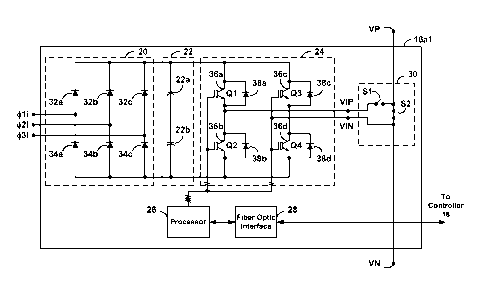
Referring now to FIG. 2A, an example power cell
(e.g., power cell 16a1) in accordance with this invention
is described. Power cell 16a1 converts a three-phase AC
input signal at input terminals 4)1i, 4)2i, 4)31 to a single
phase AC output signal at output terminals VP and VN. In
particular, power cell 16a1 includes a rectifier 20, a DC
bus capacitor 22 (which may include capacitors 22a
and 22b), an inverter 24, a processor 26, a fiber optic
interface 28 and a bypass device 30. Persons of ordinary
skill in the art will understand that power cells in
accordance with this invention may include additional,
fewer, or different components than the components
illustrated in FIG. 2A. In addition, persons of ordinary
skill in the art will understand that power cells in
accordance with this invention may include four-quadrant
("4-Q") power cells, as are known in the art.
Rectifier 20 includes diodes 32a, 32b, 32c and 34a,
34b, 34c coupled to input terminals 4)1i, 4)2i, 4)3i, and
converts a three-phase AC input signal to a substantially
constant DC voltage coupled to DC bus capacitors 22a
and 22b. Persons of ordinary skill in the art will
understand that DC bus capacitors 22a and 22b may include a
capacitor bank, and that the specific amount of capacitance
necessary depends on each particular application.
Inverter 24 converts the DC voltage across DC bus
capacitors 22a and 22b to an AC output at inverter output
terminals VIP and VIN. Inverter 24 may be a bridge
converter that includes semiconductor switches 36a, 36b,
36c and 36d, and diodes 38a, 38b, 38a and 38d.
Semiconductor switches 36a, 36b, 36c and 36d may be any
suitable switch element, such as isolated-gate bipolar
transistors ("IGBTs"), or other similar switch element.
Depending on the power level, various solid-state
6
81786168
components may be chosen. As shown in FIG. 2A, diodes 38a,
38b, 38a and 38d are configured across corresponding
semiconductor switches 36a, 36b, 36c and 36d, respectively.
Semiconductor switches 36a, 36b, 36c and 36d are
coupled to processor 26, which uses pulse-width modulation
("PWM") to selectively apply DC power to inverter outputs
VIP and VIN. In such a PWM operation, switches 36a, 36b,
36c and 36d can be considered either fully ON or fully OFF
as they operate. Persons of ordinary skill in the art will
understand that inverter 24 may have topologies other than
the bridge converter shown in FIG. 2A, and may use control
modes other than PWM.
Processor 26 may be coupled to controller 18 via
fiber optic interface 28. Processor 26 may be a
TMS320F2801 processor, or may be any other similar
processor. Fiber optic interface 28 may be an
AFBR 2624Z/AFBR 1624Z fiber optic receiver/transmitter
pair, or may be any other similar fiber optic interface.
Processor 26 may communicate status information regarding
power cell 16a1 to controller 18, and controller 18 may
communicate control signals to processor 26 to control
operation of power cell 16a1.
Bypass device 30 is coupled between inverter output
terminals VIP and VIN and power cell output terminals VP
and VN. Bypass device 30 may be a mechanical, electrical,
or a combination mechanical and electrical device that may
be selectively switched between a first configuration and a
second configuration. Bypass device 30 may include a
magnetic contactor, a spring-loaded contact, a pair of
anti-parallel silicon controlled rectifiers, or a pair of
series transistors, such as described in FIG. 1D and the
accompanying text of Hammond et al. U.S. Patent
No. 5,986,909 (the "909 patent"). Persons
7
CA 2883354 2020-01-08
CA 02883354 2015-02-26
WO 2014/036251 PCT/US2013/057281
of ordinary skill in the art will understand that other
circuits and/or devices may be used for bypass device 30.
In the example embodiment shown in FIG. 2A, bypass
device 30 includes a first switch Si and a second
switch S2. First switch 51 and second switch S2 may be
selectively opened and closed based on control signals (not
shown) provided by processor 26. Persons of ordinary skill
in the art will understand that alternative embodiments of
this invention may Include a bypass device that uses a
single switch. As shown in FIG. 2A, bypass device 30 is in
a first configuration, with first switch S1 closed and
second switch S2 open, and inverter output terminals VIP
and VIN coupled to power cell output terminals VP and VN,
respectively. In the first configuration, current is
conducted by power cell 16a1, and power cell 16a1 is 'not-
bypassed."
In contrast, FIG. 2B illustrates bypass device 30
in a second configuration, with first switch S1 open and
second switch S2 closed, forming a shunt path between
output terminals VP and VN of power cell 16a1. In the
second configuration, current is conducted through bypass
device 30 instead of power cell 16a1, and power cell 16a1
is "bypassed." Thus, bypass device 30 may be used to
selectively bypass and not-bypass (or 'de-bypass") power
cell 16a.
Referring again to FIG. 1, during normal operation,
each of power cells 16a1, 16a2, 16a3, . . . 16c4, and 16c5
is operational and not bypassed, and the output voltage of
each leg A, B, C is the sum of the output voltages of all
five power cells in the leg. For example, FIG. 3A
Illustrates an array of series-connected power cells 16al,
16a2, 16a3, . . . 16c4, and 16c5 that illustrate the
voltages from each leg and the phase displacement between
legs. In this illustrated example, each power cell 16a1,
8
CA 02883354 2015-02-26
WO 2014/036251 PCT/US2013/057281
16a2, 16a3, . . . 16c4, and 16c5 is capable of generating
an AC output voltage of 480V. Persons of ordinary skill in
the art will understand that power cell 16a1, 16a2, 16a3, .
. . 16c4, and 16c5 may provide other AC output voltages.
In the illustrated drawing, each power cell 16a1,
16a2, 16a3, . . . 16c4, and 16c5 is represented by a
circle, with five cells connected in each leg between
neutral point N and the respective points A, B and C. As
shown, such a multi-cell power supply can typically
generate up to approximately 2400V from point N to each of
points A, B and C. If controller 18 makes these three
voltages equal in magnitude and mutually phase displaced by
1200, then the array will produce a balanced three-phase AC
output voltage. In this case, the maximum available line-
to-line output voltage (e.g., VAC, VBA, VCB) from the array
shown in FIG. 3A is 4160V.
From time to time one or more of power cells 16al,
16a2, 16a3, . . . 16c4, and 16c5 may fault, and the faulted
power cells may be bypassed, e.g., using the corresponding
bypass device 30 shown in FIGS. 2A-2B. Under such
circumstances, the voltages from point N to each of points
A, B and C typically will no longer be equal in magnitude.
For example, if power cells 16a4 and 16a5 in FIG. 3A fault
and are bypassed, but all other power cells are fully
functional, leg A can produce a maximum output voltage
magnitude of only about 1440V above neutral, whereas legs B
and C still can produce a maximum output voltage magnitude
of about 2400V above neutral.
As is known in the art, various techniques may be
used to reconfigure the operation of multi-cell power
supply 10 when one or more power cells are bypassed. For
example, the '909 patent describes methods for
reconfiguring the operation of a multi-cell power
supply such that all not-bypassed power cells may be used
9
CA 02883354 2015-02-26
WO 2014/036251 PCT/US2013/057281
to contribute to a balanced output voltage. In particular,
by temporarily inhibiting normal operation of the multi-
cell power supply, modifying the phase angles between
phases A, B and C, and resuming operation of the multi-cell
power supply using the modified phase angles, all not-
bypassed power cells can be used to provide line-to-line
voltages VAC, VBA, VCB having equal magnitudes, and having
a mutual phase displacement of 1200 between VAC, VBA, and
VCB.
For example, as shown in FIG. 3B, if power
cells 16a4 and 16a5 fault and are bypassed, but all other
power cells remain fully functional, the phase angle
between phases B and C may be reduced to 950, and the phase
angles between phases A and C and between A and B may be
increased to 132.5% which will produce line-to-line
voltages VAC, VBA, and VCB having equal magnitudes
of 3542V, and a mutual phase displacement of 1200 between
VAC, VBA, and VCB.
Although multi-cell power supplies may remain
operational with some power cells bypassed, it is
preferable that all power cells be restored to service. In
some instances, a power cell may be bypassed as a result of
a temporary operating condition (e.g., a momentary ambient
temperature increase) that causes a power cell to fault.
If the power cell is otherwise healthy, and if the
operating condition that triggered the fault no longer
exists, it is preferable to de-bypass the previously
bypassed power cell.
Conventionally, bypassed power cells could be de-
bypassed only by stopping the multi-cell power supply (and
thereby completely shutting down power to and halting
operation of the load), disengaging the bypass in the
affected power cells, and then restarting the multi-cell
CA 02883354 2015-02-26
WO 2014/036251 PCT/US2013/057281
power supply. Such stopping and restarting procedures are
time consuming, however, and negatively impact the
efficiency of equipment and processes being driven by the
load.
In accordance with this invention, under certain
predetermined circumstances, previously bypassed power
cells of a multi-cell power supply may be de-bypassed
without stopping the multi-cell power supply. In
particular, a previously bypassed power cell may be tested
to determine if: (a) the operating condition that caused
the power cell fault is one of a predetermined number of
operating conditions, (b) the operating condition no longer
exists, and/or (c) the bypassed power cell is otherwise
functional. Based on the test results, the previously
bypassed power cell may be de-bypassed. As described in
more detail below, in accordance with this invention, the
previously bypassed power cell may be de-bypassed without
stopping the multi-cell power supply.
Referring now to FIG. 4A, an example method 50 of
this invention is described for determining whether one or
more of previously bypassed power cells 16a1, 16a2, 16a3, .
. . 16c4, and 16c5 may be de-bypassed. Method 50 may be
implemented in hardware, software or a combination of
hardware and software, such as on controller 18, or other
processor.
FIG. 5 will be used to illustrate the operation of
method 50. In particular, FIG. 5 illustrates an array of
series-connected power cells 16a1, 16a2, 16a3, . . 16c4,
16c5 in which power cells 16b4, 16c3 and 16c5 have
previously faulted and are bypassed (e.g., bypass
devices 30b4, 30c3 and 30c5 of power cells 16b4, 16c3 and
16c5, respectively, are all engaged), all remaining power
cells are operational, and the phase angles between
phases A, B and C, have been adjusted to provide line-to-
11
CA 02883354 2015-02-26
WO 2014/036251 PCT/1JS2013/057281
line voltages VAC, VBA, VCB having equal magnitudes
of 3249V, and having a mutual phase displacement of 1200
between VAC, VBA, and VCB.
Referring again to FIG. 4A, beginning at step 52, a
faulted and bypassed power cell (e.g., power cell 16b4) is
queried to determine if the power cell can report the
operating conditions that caused the fault. For example,
processor 26 of power cell 16b4 may monitor a variety of
operating conditions (e.g., DC bus voltage, operating
temperature(s), input voltage, input current, IGBT state,
arc detection, or other similar operating conditions) of
power cell 16b4, and may report the operating conditions
via fiber optic interface 28 in response to a query from
controller 18.
Based on the response to the query, controller 18
determines if the bypassed power cell experienced one or
more predetermined operating conditions that caused the
power cell fault. For example, at steps 54a-54d,
controller 18 determines if the reported operating
conditions indicate that power cell 16b4 experienced an
overvoltage fault, an over-temperature fault, a line fault,
or a random fault, respectively.
An overvoltage fault may be indicated if the DC bus
voltage of power cell 16b4 exceeds a predetermined
threshold. An over-temperature fault may be indicated if
a monitored temperature of power cell 16b4 exceeds a
predetermined threshold. For 4-Q power cells, a line fault
may be indicated if excessive input current existed due to
a line dip. A random fault may be any fault condition
other than the specific fault conditions identified above.
Persons of ordinary skill in the art will understand that
controller 18 may determine if the reported operating
conditions indicate that the faulted power cell experienced
12
CA 02883354 2015-02-26
WO 2014/036251 PCT/US2013/057281
additional, fewer or alternative fault conditions than the
predetermined faults described above.
Thus, at step 54a, if the reported operating
conditions indicate that power cell 16b4 experienced an
overvoltage fault, the process proceeds to step 56a, and
controller 18 determines if the overvoltage fault was the
result of regeneration. If multi-cell power supply 10
absorbs regenerative power from load 12, the DC bus voltage
of all non-bypassed power cells increases. As a result,
the most sensitive power cell will fault (e.g., power cell
16b4).
When such an ovdervoltage fault occurs, multi-cell
power supply 10 will temporarily inhibit normal operation,
bypass faulted power cell 16b4, modify the phase angles
between phases A, B and C, and resume operation of multi-
cell power supply 10 (assuming that the remaining non-
bypassed power cells do not similarly experience an over-
voltage fault) using the modified phase angles as described
above. While multi-cell power supply 10 is temporarily
inhibited, the remaining non-bypassed power cells will
cease acceptance of regenerative power, which will cause
the DC bus voltage to drop. Multi-cell power supply 10
will resume operation, but faulted power cell 16b4 remains
bypassed.
If such an overvoltage fault was not a result of a
defective power cell (e.g., one that should remain bypassed
until it can be replaced), but instead resulted because
multi-cell power supply 10 absorbed regenerative power from
load 12, bypassed power cell 16b4 may be de-bypassed.
Thus, at step 56a, controller 18 determines if
multi-cell power supply 10 absorbed regenerative power from
load 12 prior to the overvoltage fault of power cell 16b4.
For example, controller 18 may query all other non-bypassed
power cells 16a1, 16a2, 16a3, . . 16c2, and 16c4 to
13
CA 02883354 2015-02-26
WO 2014/036251 PCT/US2013/057281
determine if those power cells also experienced increased
DC bus voltages prior to the fault of power cell 16b4.
Alternatively, or additionally, controller 18 may determine
if multi-cell power supply 16 absorbed power from load 12
prior to the fault on power cell 16b4.
If either or both tests indicated that multi-cell
power supply 10 absorbed regenerative power from load 12
prior to the overvoltage fault of power cell 16b4, the
process proceeds to step 58 to de-bypass power cell 16b4.
If one or both test fail to indicate regeneration, the
process proceeds to step 60 to continue bypassing power
cell 16b4.
Referring again to step 54a, if the reported
operating conditions indicate that power cell 16b4 did not
experience an overvoltage fault, the process proceeds to
step 54b, and controller 18 determines if the reported
operating conditions indicate that power cell 16b4
experienced an over-temperature fault.
If multi-cell power supply 10 temporarily
overheats, the most sensitive power cell typically will
fault (e.g., power cell 16b4). As a result, multi-cell
power supply 10 will temporarily inhibit normal operation,
bypass faulted power cell 16b4, modify the phase angles
between phases A, B and C, and resume operation of multi-
cell power supply 10 (assuming that the remaining non-
bypassed power cells do not experience an over-temperature
fault) using the modified phase angles as described above.
If such an over-temperature fault was not a result
of a defective power cell (e.g., one that should remain
bypassed until it can be replaced), but instead resulted
because multi-cell power supply 10 temporarily overheated,
and if power cell 16b4 has subsequently cooled, bypassed
power cell 16b4 may be de-bypassed.
14
CA 02883354 2015-02-26
WO 2014/036251 PCT/US2013/057281
Thus, at step 56b, controller 18 determines if
multi-cell power supply 10 temporarily overheated prior to
the over-temperature fault of power cell 16b4. For
example, controller 18 may query all of the power cells
16a1, 16a2, 16a3, . . 16c2, and 16c4 to determine if the
power cells experienced an increase in temperature prior to
the fault of power cell 16b4, and are no longer at an
increased operating temperature.
If the test indicates that multi-cell power
supply 10 temporarily overheated prior to the over-
temperature fault of power cell 16b4, and that all power
cells are no longer at an increased operating temperature,
the process proceeds to step 58 to de-bypass power
cell 16b4. If the test fails to indicate temporary
overheating, the process proceeds to step 60 to continue
bypassing power cell 16b4.
Referring again to step 54b, if the reported
operating conditions indicate that power cell 16b4 did not
experience an over-temperature fault, the process proceeds
to step 54c, and controller 18 determines if the reported
operating conditions indicate that power cell 16b4
experienced a line fault.
If a line disturbance occurs on the AC Source that
drives multi-cell power supply 10, the most sensitive power
cell typically will fault (e.g., power cell 16b4). As a
result, multi-cell power supply 10 will temporarily inhibit
normal operation, bypass faulted power cell 16b4, modify
the phase angles between phases A, B and C, and resume
operation of multi-cell power supply 10 (assuming that the
remaining non-bypassed power cells do not similarly
experience a line fault) using the modified phase angles as
described above.
If such a line fault was not a result of a
defective power cell (e.g., one that should remain bypassed
CA 02883354 2015-02-26
WO 2014/036251 PCT/US2013/057281
until it can be replaced), but instead resulted because
multi-cell power supply 10 experienced a temporary line
disturbance, bypassed power cell 16b4 may be de-bypassed.
Thus, at step 56c, controller 18 determines if
multi-cell power supply 10 experienced a temporary line
disturbance prior to the line fault of power cell 16b4.
For example, controller 18 may monitor the input current,
input voltage and/or input power flow to multi-cell power
supply 10 to check for excursions prior to the fault of
power cell 16b4.
If the test indicates that prior to the fault of
power cell 16b4, the input voltage varied greatly from
nominal, or the input current changed by more than what
could be produced by a single power cell, or if the input
power changed by more than what could be produced by a
single power cell, the process proceeds to step 58 to de-
bypass power cell 16b4. If the test fails to indicate such
input current, input voltage or input power excursions, the
process proceeds to step 60 to continue bypassing power
cell 16b4.
Referring again to step 54c, if the reported
operating conditions indicate that power cell 16b4 did not
experience a line disturbance, the process proceeds to
step 54d, and controller 18 determines if power cell 16b4
experienced a temporary random fault, but is otherwise
functional. If the fault of power cell 16b4 was not a
result of a defective power cell (e.g., one that should
remain bypassed until it can be replaced), but instead
resulted from some random reason, bypassed power cell 16b4
may be de-bypassed.
Thus, at step 56d, controller 18 determines if
power cell 16b4 is functional. For example, while power
cell 16b4 remains bypassed, controller 18 may test the
voltage blocking capability of semiconductor switches 36a,
16
CA 02883354 2015-02-26
WO 2014/036251 PCT/US2013/057281
36b, 36c and 36d of inverter 24 of power cell 16b4 to
determine if the switches are functioning properly.
For example, referring to FIG. 2A, a resistor and
opto-coupler (not shown) may be placed in parallel with
each of semiconductor switches 36a, 36b, 36c and 36d to
monitor the voltage across each switch. Controller 18 (via
processor 26) may then turn OFF each of semiconductor
switches 36a, 36b, 36c and 36d to determine if all four
switches effectively block voltage, and then individually
turn ON semiconductor switches 36a, 36b, 36c and 36d to
determine if each switch conducts when requested.
Referring again to FIG. 471, if all semiconductor
switches 36a, 36b, 36c and 36d block voltage when turned
OFF, and conduct current when turned ON, the process
proceeds to step 58 to de-bypass power cell 16b4. If the
test indicates that any of semiconductor switches 36a, 36b,
36c and 36d fail to properly turn OFF and ON, the process
proceeds to step 60 to continue bypassing power cell 16b4.
Following steps 58 and 60, the process proceeds to
step 62 to determine if any additional power cells 16a1,
16a2, 16a3, . . 16c2, and 16c4 have been bypassed (e.g.,
power cells 16c3 and 16c5 in FIG. 5). If additional power
cells have been bypassed, the process returns to step 52,
and determines if the additional faulted power cell
experienced one or more predetermined fault conditions.
Persons of ordinary skill in the art will
understand that the sequence of steps 54a-54d may be
rearranged in any sequence. In addition, persons of
ordinary skill in the art will understand that example
processes in accordance with this invention may test more
than one faulted power cell at a time, and may de-bypass
more than one faulted power cell at a time.
In addition, as shown in FIG. 4B, in an alternative
example process 50', step 56d (determining if all
17
CA 02883354 2015-02-26
WO 2014/036251
PCT/US2013/057281
semiconductor switches 36a, 36b, 36c and 36d block voltage
when turned OFF, and conduct current when turned ON) may be
Implemented in all Instances prior to de-bypassing a power
cell without stopping multi-cell power supply 10. This may
serve as an additional safeguard to confirm that power
cells that have faulted as a result of regeneration,
temporary over-heating and/or line disturbances may safely
be de-bypassed.
As described above in FIGS. 4A and 4B, at step 58,
a previously bypassed power cell may be de-bypassed.
Referring now to FIG. 6, an example process 70 in
accordance with this invention is described for de-
bypassing a previously bypassed power cell without stopping
multi-cell power supply 10.
Beginning at step 72, the operation of multi-cell
power supply 10 is temporarily inhibited. For example,
referring to FIGS. 1 and 2, controller 18 may inhibit
operation of multi-cell power supply 10 by inhibiting
gating signals to semiconductor switches 36a, 36b, 36c and
36d of each Inverter 24 of each of power cells 16a1, 16a2,
16a3, . . 16c4, 16c5. By doing so, semiconductor
switches 36a, 36b, 36c and 36d of multi-cell power supply
stop switching, and no voltage is supplied to load 12 by
multi-cell power supply 10.
Referring again to FIG. 6, at step 74, bypass
device 30 of the faulted power cell (e.g., power cell 16b4)
is reconfigured to de-bypass power cell 16b4, thus
reconfiguring the array of series-connected power cells
168.1, 16a2, 16a3, . . 16c4, 16c5. For
example, FIG. 7A
illustrates an array of series-connected power cells 16a1,
16a2, 16a3, . . 16c4, 16c5
in which bypass device 30b4
is reconfigured to de-bypass power cell 16b4.
Referring again to FIG. 6, at step 76, modified
phase angles between phases A, B and C are determined for
18
CA 02883354 2015-02-26
WO 2014/036251
PCT/US2013/057281
the reconfigured array of series-connected power cells
16a1, 16a2, 16a3, . . 16c4, 16c5.
As described in the
'909 patent, the required phase angles between phases A, B
and C depend on the number of functional power cells in
each phase. For example, controller 18 may calculate
specific phase angles for each configuration of the array
of series-connected power cells 16a1, 16a2, 16a3, . .
16c4, 16c5. Alternatively, controller 18 may store (e.g.,
in one or more lookup tables) predetermined phase angle
relationships for various configurations of the array of
series-connected power cells 16a1, 16a2, 16a3, . . 16c4,
16c5.
Referring now to FIGS. 8A-8G3, example table values
of the leg-to-leg phase relationship for multi-cell power
supplies utilizing anywhere from two to eight power cells
per leg. In these tables, the legs are assumed to be in a
three-phase Y arrangement having legs A, B and C. Each
table has been abbreviated to provide the same values
without regard to which power cell in a given leg is
bypassed. For example, in FIG. 8A, a leg having
A cells = 1, corresponds to any configuration in which one
of the two power cells in a two power cell leg has been
bypassed.
In addition, because a bypass condition in a multi-
cell power supply results in identical phase relationships
without regard to which legs have the number of bypassed
power cells, a multi-cell power supply with A=5, B=3 and
C=5, is the same as a multi-cell power supply having non-
bypassed cells A=5, B=5 and C=3. The tables, therefore,
provide an easy reduced form to cover all of these
combinations. In the tables, the A cell is always listed
as having the most non-bypassed power cells, the B, second
most non-bypassed power cells, and C the least non-bypassed
power cells. The tables may be used in a microprocessor
19
CA 02883354 2015-02-26
WO 2014/036251 PCT/US2013/057281
scheme as lookup tables to determine the proper phase
relationship in a power supply having bypassed power cells.
In the tables, the term Vmax % is used to indicate
the maximum voltage that would be available under a
bypassed condition as a percentage of the normal line-to-
line voltage. All of the phase angles are in relationship
to the normal A vector in a multi-cell power supply having
no bypassed cells. As an example, Ap is the angle between
the A leg in a bypassed mode as compared to the A leg in an
un-bypassed mode. All of the angles given are in relation
to the vector for the A leg in an un-bypassed mode.
Thus, for example, referring to FIGS. 7A and 8D,
with bypass device 30b4 reconfigured to de-bypass power
cell 16b4, multi-cell power supply 10 corresponds to an
A=5, B=5 and C=3 configuration, in which Vmax % = 85.1, Ap
= 12.5 , Bp = 107.5 , and Cp = 240 . Thus, as shown in
FIG. 7A, the phase angle between phase A and phase B is
(107.5 - 12.5 ) - 95 , the phase angle between phase B and
phase C is (240 - 107.5 ) = 132.5 , and the phase angle
between phase C and phase A is (372.5 - 240 ) = 132.5 .
Referring again to FIG. 6, at step 78,
controller 18 resumes the operation of multi-cell power
supply 10. As shown in FIG. 7A, with power cell 16b4 de-
bypassed, multi-cell power supply 10 provides line-to-line
voltages VAC, VBA, VCB having equal magnitudes of 3542V
(85.1% of 4160V), and having a mutual phase displacement
of 120 between VAC, VBA, and VCB. In this regard,
previously bypassed power cell 16b4 has been de-bypassed
without stopping multi-cell power supply 10.
Persons of ordinary skill in the art will
understand that the time required to temporarily Inhibit
multi-cell power supply 10, de-bypass previously bypassed
power cell 16b4, determine modified phase angles between
CA 02883354 2015-02-26
WO 2014/036251 PCT/US2013/057281
phases A, B and C, and resume operation of multi-cell power
supply 10 is very brief, e.g., between about 100 ms to
about 350 ms, or other similar duration. During this time
interval, load 12 rides-through this power interruption due
to the inertia of the load. If there is low inertia,
load 12 may slow down significantly. However, unlike
previous techniques, methods in accordance with this
Invention do not stop multi-cell power supply 10, which
would completely shut down power to and halt operation of
load 12.
Example process 70 of FIG. 6 may be repeated with
previously bypassed power cell 16c3. Thus, at step 72, the
operation of multi-cell power supply 10 is inhibited, and
at step 74, bypass device 30 of a faulted power cell (e.g.,
power cell 16c3) is reconfigured to de-bypass power
cell 16c3, thus reconfiguring the array of series-connected
power cells 16a1, 16a2, 16a3, . . 16c4, 16c5. For
example, FIG. 7B illustrates an array of series-connected
power cells 16a1, 16a2, 16a3, . . 16c4, 16c5 in which
previously bypassed power cell 16c3 is de-bypassed.
Referring again to FIG. 6, at step 76, modified
phase angles between phases A, B and C are determined for
the reconfigured array of series-connected power cells
16a1, 16a2, 16a3, . . 16c4, 16c5. Referring to FIGS. 7B
and 8D, with bypass device 30c3 of power cell 16c3
reconfigured to de-bypass power cell 16c3, multi-cell power
supply 10 corresponds to an A=5, B=5 and C=4 configuration,
in which Vmax % - 92.9, Ap = 6.40, Bp = 113.6 , and Cp =
240'. Thus, as shown in FIG. 7B, the phase angle between
phase A and phase B is (113.6 - 6.4 ) = 107.2 , the phase
angle between phase B and phase C is (240 - 113.6 ) =
126.4 , and the phase angle between phase C and phase A is
(366.4 - 240 ) = 126.4 .
21
CA 02883354 2015-02-26
WO 2014/036251
PCT/US2013/057281
Referring again to FIG. 6, at step 78,
controller 18 resumes the operation of multi-cell power
supply 10. As shown in FIG. 7B, with power cell 16c3 de-
bypassed, multi-cell power supply 10 provides line-to-line
voltages VAC, VBA, VCB having equal magnitudes of 3865V
(92.9% of 4160V), and having a mutual phase displacement
of 1200 between VAC, VBA, and VCB. In this regard,
previously bypassed power cell 16c3 has been de-bypassed
without stopping multi-cell power supply 10.
Likewise, example process 70 of FIG. 6 may be
repeated with previously bypassed power cell 16c5. Thus,
at step 72, the operation of multi-cell power supply 10 is
inhibited, and at step 74, bypass device 30 of a faulted
power cell (e.g., power cell 16c5) is reconfigured to de-
bypass power cell 16c5, thus reconfiguring the array of
series-connected power cells 16a1, 16a2, 16a3, . . 16c4,
16c5. For example, FIG. 7C illustrates an array of series-
connected power cells 16a1, 16a2, 16a3, . . 16c4, 16c5
in which previously bypassed device 30c5 of power cell 16c5
is reconfigured to de-bypass power cell 16c5.
Referring again to FIG. 6, at step 76, modified
phase angles between phases A, B and C are determined for
the reconfigured array of series-connected power cells
16a1, 16a2, 16a3, . . 16c4, 16c5.
Referring to FIGS. 7C
and 8D, with bypass device 30c5 of power cell 16c5
reconfigured to de-bypass power cell 16c5, multi-cell power
supply 10 corresponds to an A=5, B=5 and C=5 configuration,
in which Vmax % = 100, Ap = 00, Bp = 120 , and Cp = 240 .
Thus, as shown in FIG. 7C, the phase angle between phase A
and phase B is (120' - 0 ) = 120 , the phase angle between
phase B and phase C is (240 - 1200) = 120 , and the phase
angle between phase C and phase A is (3600 - 240 ) = 120 .
22
CA 02883354 2015-02-26
WO 2014/036251 PCT/US2013/057281
Referring again to FIG. 6, at step 78,
controller 18 resumes the operation of multi-cell power
supply 10. As shown in FIG. 70, with power cell 16c5 de-
bypassed, multi-cell power supply 10 provides line-to-line
voltages VAC, VBA, VCB having equal magnitudes of 4160V
(100% of 4160V), and having a mutual phase displacement
of 1200 between VAC, VBA, and VCB. In this regard,
previously bypassed power cell 16c5 has been de-bypassed
without stopping multi-cell power supply 10.
Persons of ordinary skill in the art will
understand that other techniques (e.g., the alternative
techniques described in the '909 patent) may be used to
determine phase angles between phases A, B and C of the
reconfigured array of series-connected power cells 16a1,
16a2, 16a3, . . 16c4, 16c5 so that a previously bypassed
power cell may he de-bypassed without stopping multi-cell
power supply 10.
The foregoing merely illustrates the principles of
this invention, and various modifications can be made by
persons of ordinary skill in the art without departing from
the scope and spirit of this invention.
23