Note : Les descriptions sont présentées dans la langue officielle dans laquelle elles ont été soumises.
LENSES WITH ELECTRICALLY-TUNABLE POWER AND ALIGNMENT
FIELD OF THE INVENTION
The present invention relates generally to optical devices, and particularly
to electrically-tunable
lenses.
BACKGROUND
Tunable lenses are optical elements whose optical characteristics, such as the
focal length and/or
the location of the optical axis, can be adjusted during use, typically under
electronic control. Such lenses
may be used in a wide variety of applications. For example, U.S. Patent
7,475,985 describes the use of an
electro-active lens for the purpose of vision correction.
Electrically-tunable lenses typically contain a thin layer of a suitable
electro-optical material, i.e.,
a material whose local effective index of refraction changes as a function of
the voltage applied across the
material. An electrode or array of electrodes is used to apply the desired
voltages in order to locally adjust
the refractive index to the desired value. Liquid crystals are the electro-
optical material that is most
commonly used for this purpose (wherein the applied voltage rotates the
molecules, which changes the
axis of birefringence and thus changes the effective refractive index), but
other materials, such as polymer
gels, with similar electro-optical properties can alternatively be used for
this purpose.
Various designs for lenses based on liquid crystals are known in the art,
although their practical
uses have been limited. For example, Naumov et al. describe one approach for
this purpose in "Liquid-
Crystal Adaptive Lenses with Modal Control," Optics Letters 23, pages 992-994
(1998). The authors used
nematic liquid-crystal (LC) phase correctors to form spherical and cylindrical
wave fronts. A LC cell with
a distributed reactive electrical impedance was driven by an AC voltage
applied to the cell boundary to
yield the desired spatial distribution of the refractive index.
Other tunable lens designs use an electrode array to define a grid of pixels
in the liquid crystal,
similar to the sort of pixel grid used in liquid-crystal displays. The
refractive indices of the individual
pixels may be electrically controlled to give a desired phase modulation
profile. (The term "phase
modulation profile" is used in the present description and in the claims to
CA 2884212 2019-10-30 1
CA 02884212 2015-03-05
WO 2014/049577 PCT/IB2013/058989
mean the distribution of the local phase shifts that are applied to light
passing through the layer
as the result of the locally-variable effective refractive index over the area
of the electro-optical
layer of the tunable lens.) Lenses using grid arrays of this sort are
described, for example, in
the above-mentioned U.S. Patent 7,475,985.
SUMMARY
Embodiments of the present invention that are described hereinbelow provide
improved
electronically-tunable optical devices.
There is therefore provided, in accordance with an embodiment of the present
invention,
an optical device, including an electro-optical layer, having a local
effective index of refraction
at any given location within an active area of the electro-optical layer that
is determined by a
voltage waveform applied across the electro-optical layer at the location. A
common electrode
is positioned over the active area on a first side of the electro-optical
layer. An array of
excitation electrodes, including parallel conductive stripes, extends over the
active area on a
second side of the electro-optical layer, opposite the first side. Control
circuitry is coupled to
apply respective control voltage waveforms to the excitation electrodes and is
configured to
concurrently modify the respective control voltage waveforms applied to a
plurality of the
excitation electrodes, thereby modifying a phase modulation profile of the
electro-optical layer.
In some embodiments, the control circuitry is configured to apply the control
voltage
waveforms to the excitation electrodes so that the device functions as a
cylindrical lens,
possible a cylindrical Fresnel lens, having focal properties determined by the
phase modulation
profile. Typically, the control circuitry is configured to modify the control
voltage waveforms
applied to the excitation electrodes so as to change a focal length of the
cylindrical lens and/or
to shift a focal line of the cylindrical lens in a direction transverse to the
device.
In disclosed embodiments, the electro-optical layer includes a liquid crystal,
which may
be configured as a polarization-independent layer.
There is also provided, in accordance with an embodiment of the present
invention,
apparatus including first and second optical devices as described above,
wherein the first and
second optical devices are arranged in series. The electrodes of the first and
second optical
devices may share a common substrate. In a disclosed embodiment, the
excitation electrodes in
the second optical device are oriented in a direction orthogonal to the
excitation electrodes in
the first optical device, and the control circuitry may be configured to apply
the control voltages
to the excitation electrodes in the first and second optical devices so that
the apparatus emulates
2
CA 02884212 2015-03-05
WO 2014/049577 PCT/IB2013/058989
a spherical lens. Optionally, the control circuitry may modify the control
voltages applied to
the excitation electrodes so as to shift an optical axis of the spherical
lens.
Alternatively, the electro-optical layer in the first optical device has a
first birefringence
axis, and the electro-optical layer in the second optical device has a second
birefringence axis,
perpendicular to the first birefringence axis.
There is additionally provided, in accordance with an embodiment of the
present
invention, an ophthalmic lens system including the device as described above.
There is further provided, in accordance with an embodiment of the present
invention,
an optical device, including an electro-optical layer, having an effective
local index of
refraction at any given location within an active area of the electro-optical
layer that is
determined by a voltage waveform applied across the electro-optical layer at
the location. A
first array of first excitation electrodes, including first parallel
conductive stripes, extends in a
first direction over the active area on a first side of the electro-optical
layer. A second array of
second excitation electrodes, including second parallel conductive stripes,
extends in a second
direction, orthogonal to the first direction, over the active area on a second
side of the electro-
optical layer, opposite the first side. Control circuitry is coupled to apply
respective control
voltage waveforms to the excitation electrodes and is configured to
concurrently modify the
respective control voltage waveforms applied to both the first excitation
electrodes and the
second excitation electrodes so as to generate a specified phase modulation
profile in the
electro-optical layer.
In disclosed embodiments, the control circuitry is configured to apply the
control
voltage waveforms at different, respective amplitudes to different ones of the
excitation
electrodes and/or with different, respective duty cycles to different ones of
the excitation
electrodes.
In some embodiments, the control circuitry is configured to apply the control
voltage
waveforms to the excitation electrodes so that the device functions as a lens,
such as a Fresnel
lens, having focal properties determined by the phase modulation profile.
Typically, the control
circuitry is configured to modify the control voltage waveforms applied to the
excitation
electrodes so as to change a focal length of the lens and/or to shift an
optical axis of the lens.
The control circuitry may apply the voltage waveforms to the excitation
electrodes so that the
device functions as an astigmatic spherical lens.
In one embodiment, the control circuitry is configured to apply the control
voltage
waveforms so that the voltage applied across the electro-optical layer is
constrained to be within
3
CA 02884212 2015-03-05
WO 2014/049577 PCT/IB2013/058989
a range in which the local effective index of refraction varies as a quasi-
linear function of the
applied voltage.
In another embodiment, the phase modulation profile is defined as a function
that is
separable into first and second component functions, which respectively vary
along first and
second axes aligned in the second and first directions, respectively, and the
control voltage
waveforms applied to the first and second excitation electrodes are specified
in accordance with
the first and second component functions, respectively. The first and second
component
functions may be defined in terms of a set of component waveforms that are
selected so as to
correspond to different, respective phase shifts in the electro-optical layer,
such that the phase
modulation profile includes a sum of the respective phase shifts due to the
first and second
component functions at each location within the active area.
There is moreover provided, in accordance with an embodiment of the present
invention, apparatus including first and second optical devices as described
above, wherein the
first and second optical devices are arranged in series, possibly with
perpendicular
birefringence axes.
There is furthermore provided, in accordance with an embodiment of the present
invention, an optical device, including an electro-optical layer, having a
local effective index of
refraction at any given location within an active area of the electro-optical
layer that is
determined by a voltage applied across the electro-optical layer at the
location. The electro-
optical layer has first and second sides and a layer thickness equal to a
distance between the
first and second sides. Conductive electrodes extend over the first and second
sides of the
electro-optical layer. The electrodes include at least one array of excitation
electrodes having
an inter-electrode pitch that is less than four times the layer thickness of
the electro-optical
layer. Control circuitry is coupled to apply control voltage waveforms to the
excitation
electrodes so as to modify a phase modulation profile of the electro-optical
layer.
In a disclosed embodiment, the electrodes include parallel stripes of a
transparent
conductive material having gaps between the stripes of a gap width that is
less than the layer
thickness of the electro-optical layer.
There is also provided, in accordance with an embodiment of the present
invention, a
method for producing an optical device. The method includes providing an
electro-optical
layer, having a local effective index of refraction at any given location
within an active area of
the electro-optical layer that is determined by a voltage waveform applied
across the electro-
optical layer at the location. A common electrode is positioned on a first
side of the electro-
4
CA 02884212 2015-03-05
WO 2014/049577 PCT/IB2013/058989
optical layer, so as to cover the active area. An array of excitation
electrodes, including parallel
conductive stripes, is positioned so as to extend over the active area on a
second side of the
electro-optical layer, opposite the first side. Control circuitry is coupled
to apply respective
control voltage waveforms to the excitation electrodes and to concurrently
modify the control
voltage waveforms applied to a plurality of the excitation electrodes, thereby
modifying a phase
modulation profile of the electro-optical layer.
There is additionally provided, in accordance with an embodiment of the
present
invention, a method for producing an optical device, which includes providing
an electro-
optical layer, having a local effective index of refraction at any given
location within an active
area of the electro-optical layer that is determined by a voltage waveform
applied across the
electro-optical layer at the location. A first array of first excitation
electrodes, including first
parallel conductive stripes, is positioned so as to extend in a first
direction over the active area
on a first side of the electro-optical layer. A second array of second
excitation electrodes,
including second parallel conductive stripes, is positioned so as to extend in
a second direction,
orthogonal to the first direction, over the active area on a second side of
the electro-optical
layer, opposite the first side. Control circuitry is coupled to apply
respective control voltage
waveforms to the excitation electrodes and to concurrently modify the control
voltage
waveforms applied to both the first excitation electrodes and the second
excitation electrodes so
as to generate a specified phase modulation profile in the electro-optical
layer.
There is further provided, in accordance with an embodiment of the present
invention, a
method for producing an optical device. The method includes providing an
electro-optical
layer, having a local effective index of refraction at any given location
within an active area of
the electro-optical layer that is determined by a voltage applied across the
electro-optical layer
at the location, the electro-optical layer having first and second sides and a
layer thickness equal
to a distance between the first and second sides. Conductive electrodes are
positioned so as to
extend over the first and second sides of the electro-optical layer, the
electrodes including at
least one array of excitation electrodes having an inter-electrode pitch that
is less than four
times the layer thickness of the electro-optical layer. Control circuitry is
coupled to apply
control voltage waveforms to the excitation electrodes so as to modify a phase
modulation
profile of the electro-optical layer.
The present invention will be more fully understood from the following
detailed
description of the embodiments thereof, taken together with the drawings in
which:
CA 02884212 2015-03-05
WO 2014/049577 PCT/IB2013/058989
BRIEF DESCRIPTION OF THE DRAWINGS
Fig. 1 is schematic side view of an optical system, in accordance with an
embodiment of
the present invention;
Fig. 2A is a schematic, pictorial illustration of an optical device, in
accordance with an
embodiment of the present invention;
Figs. 2B and 2C are schematic side views of electrodes disposed on opposing
sides of
the device of Fig. 2A, in accordance with an embodiment of the present
invention;
Fig. 3A is a schematic, pictorial illustration of an optical device, in
accordance with
another embodiment of the present invention;
Figs. 3B and 3C are schematic side views of electrodes formed on opposing
sides of the
device of Fig. 3A, in accordance with an embodiment of the present invention;
Fig. 3D is a schematic side view of the device of Fig. 3A, showing a
superposition of
the electrodes on the opposing sides of the device, in accordance with an
embodiment of the
present invention; and
Fig. 4 is a schematic plot showing the dependence of the effective refractive
index of a
liquid crystal layer in an optical device as a function of applied voltage,
used in controlling an
optical device in accordance with an embodiment of the present invention.
DETAILED DESCRIPTION OF EMBODIMENTS
OVERVIEW
Electrically-tunable lenses using an electro-optical material with a pixel
grid can, in
principle, generate any desired phase modulation profile, within the limits of
the achievable
range of the local refractive index and the pitch of the pixels. Realization
of practical lenses for
many applications, however, such as for ophthalmic use, requires a large
addressable grid of
very small pixels, for example, an array of at least 400 X 400 pixels with a
pitch of 50 p m or
less.
In liquid-crystal display (LCD) panels, the pixels are typically arranged in a
matrix of N
rows and M columns. Each of the N*M pixels can receive a set of possible
values (gray levels),
independent of all other pixels. Different pixel values are obtained by
altering the local
voltages applied to the liquid crystal (LC) layer. Typically the voltage is
time-varying and
alternating in sign (AC), at a rate faster than the LC response time, and the
LC responds to the
effective average applied voltage, as long as the average voltage is above a
certain threshold.
6
CA 02884212 2015-03-05
WO 2014/049577 PCT/IB2013/058989
The effective voltages applied to the LCD panel pixels are controlled by
driving
circuitry. Due to the large pixel count, the driving circuitry typically
controls the voltages of
column and row electrodes and does not directly control the voltage on each
pixel. This
scheme enables the driver to control only N+M, instead of N*M, voltage values.
Since it is
necessary to control the effective voltage on each pixel independently, time-
sharing techniques
are used in the driver to update the values of the pixels serially. Row
electrodes are typically
used for control voltages, selecting an active row, while column electrodes
are used to apply
data-dependent voltages, corresponding to the required values of the pixels in
the currently-
active row that is selected by the row control voltage. The required pixel
values of a certain
column are thus multiplexed over the column voltage waveforms.
Time-sharing of this sort can be achieved, for example, by placing a
transistor beside
every pixel. The transistor connects the column electrode to the pixel
electrode, and its
conductivity is controlled by the corresponding row electrode. Rows are thus
addressed
serially, one row at a time. When a certain row, for example row number k, is
to be updated,
the voltage of the k row electrode is set to open the transistors of the
pixels of that row, while
all other row voltages are set to close the transistors. The column electrode
voltages are then
updated according to the data to be displayed in row k. Although panels of
this sort are capable
of implementing a lens, the relatively low pixel fill factor, due to the
transistors, produces
diffractive effects that limit the lens quality.
Time-sharing can also be implemented without resorting to transistors. In this
scheme,
known as time-division multiplexing, the LC layer is positioned between two
arrays of parallel
electrodes, oriented orthogonally. The X-axis electrodes are positioned on one
side of the LC,
and the Y-axis electrodes, orthogonal to the X-axis electrodes, are positioned
on the other side
of the LC. The voltage on each pixel is thus the difference between the
voltage waveforms of
its row and column electrodes. In order to achieve the desired phase
modulation profile, the
voltages of all row electrodes except for the row that is to be updated are
set to a value Vbias,
which is chosen to ensure that the voltage difference between Vbias and the
column electrode
voltages is below the LC response threshold voltage. Only the pixels in the
row that is to be
updated receive voltages that are larger than the LC threshold voltage, and
are thus updated.
This scheme, however, cannot support large pixel counts, and therefore cannot
be used to
implement a high quality lens.
Embodiments of the present invention that are described herein overcome the
above
limitations by providing novel electrically-tunable optical devices that are
able to achieve finer
7
CA 02884212 2015-03-05
WO 2014/049577 PCT/IB2013/058989
pitch and more flexible addressability than devices that are known in the art.
For example, the
disclosed devices may be configured to operate as cylindrical lenses (with
focusing along one
axis, using an array of stripe electrodes) or to emulate spherical lenses,
with dual-axis focusing.
Both the focal power and the location of the optical axis, i.e., the effective
central point or axis
of the lens defined in this manner, can be changed freely and rapidly by
application of
appropriate control voltages.
Generally speaking, the disclosed devices can be configured to apply any phase
modulation profile that is separable. A two dimensional phase modulation
profile e i0(x,y) is
separable if it can be decomposed into a product of two one-dimensional
functions,
ei0(x Y) p
¨ x
i0(x) .
' ¨ e Y(Y). In other words, these devices are able to apply
any
phase modulation profile that is defined as a function that is separable into
two component
functions that vary along respective, mutually-orthogonal axes, and the phase
modulation
profile will then comprise a sum of the respective phase shifts due to the
first and second
component functions. (As phase is a cyclical function, with period 27r, the
term "sum" should
be understood in this context as including modular summation, with modulo
27r.)
In some of the disclosed embodiments, an optical device comprises an electro-
optical
layer, meaning, as explained above, that the local effective index of
refraction at any given
location within the active area of the layer is determined by the voltage
applied across the layer
in the vicinity of the location. Typically, the electro-optical layer
comprises a liquid crystal,
possibly a polarization-independent liquid crystal layer (such as a
cholesteric LC layer),
although other types of electro-optical materials may alternatively be used. A
common
electrode is positioned over the active area on one side of the electro-
optical layer. An array of
excitation electrodes, comprising parallel stripes of a conductive material,
extends over the
active area on the opposite side of the electro-optical layer.
To drive and modify the phase modulation profile of the electro-optical layer,
control
circuitry applies respective control voltages to the excitation electrodes.
Typically, each stripe
(i.e., each excitation electrode) is individually connected to and controlled
by the control
circuitry, so that the voltage waveforms applied to several or even all of the
excitation
electrodes can be modified concurrently. This configuration provides an
optical element of
arbitrary, tunable one-dimensional profile (such as a cylindrical lens), with
a resolution limited
only by the distance between the stripes and the thickness of the electro-
optical layer. The
8
CA 02884212 2015-03-05
WO 2014/049577 PCT/IB2013/058989
phase modulation properties of the device can be modified at a rate limited
only by the speed of
the control circuitry and the response time of the electro-optical layer.
Two devices of this type may be superimposed at right angles, with the
excitation
electrodes in one device oriented in a direction orthogonal to those in the
other device, in order
to provide apparatus capable of emulating a spherical lens under the paraxial
approximation.
In other embodiments, an optical device comprises an electro-optical layer
with first and
second arrays of excitation electrodes on opposite sides of the layer. Each of
the arrays
comprises parallel stripes of a conductive material extending over the active
area, with the
second array oriented in a direction orthogonal to the first array. Control
circuitry applies
respective control voltage waveforms to the excitation electrodes in both
arrays and is capable
of modifying the control voltages applied to multiple excitation electrodes
(and possibly all of
the excitation electrodes) on both of the sides of the electro-optical layer.
The control circuitry
may concurrently modify the respective control voltage waveforms applied to
the excitation
electrodes in both the first and second arrays so as to generate a specified
phase modulation
profile in the electro-optical layer.
In these embodiments, no time-division multiplexing scheme is required, and
both row
and column voltage waveforms are data-dependent. The voltage waveforms are
chosen to
create a linear phase response in the electro-optical material. Formally
stated, the term "linear
phase response," used in connection with voltage waveforms applied to the LC,
means that
when a set of voltages waveforms fl7x,1 (t) N. 1 is applied to a first set of
electrodes,
=
corresponding to a first predefined set of phase values {0x,i}i=1, and a set
of voltage
waveforms tvy 1M is
applied to a second set of electrodes, positioned orthogonally
to the first set of electrodes, corresponding to a second predefined set of
phase values
{0y 1M 1' then for each i = ..N and j = M, the phase modulation profile T [V
(0)
j=
for light passing through the electro-optical layer when the voltage waveform
V(t) is applied to
it will be TL, tVxji (t) ¨ Vyi = e x,i11,i In
practical embodiments,
the inventors have found that sets of sixteen or more phase values (i.e., N, M
> 16) give good
results in terms of optical performance.
9
CA 02884212 2015-03-05
WO 2014/049577 PCT/IB2013/058989
For example, a spherical lens is an optical element with a transfer function
i (x2 y2)
T(x,y) = e f and A being the
lens focal length and the wavelength
Tr 2 Tr 2
i-X i-y
respectively. T(x,y) is separable, T(x,y) e Af = e
, and the total phase
response can be expressed as a sum of a phase contribution in the x axis and a
phase
contribution in the y axis. The maximal phase retardation of a lens with an
aperture radius R is
71- R 2 . The phase modulation range can be divided into N quantization
levels, Oj = ¨
Af
7 R2
Af
In some embodiments of the present invention, linear-phase-response voltage
waveforms are defined to correspond to these phase values. The required phase
modulation
value is then calculated for each electrode. For example, the electrode
positioned at X = X1
7r ,
requires a phase ¨ k.,X1 ¨ ,X0\ 2 , wherein X0 is the center point of the
lens. This phase
Af
value is quantized to the closest predefined quantization level. Denoting the
closest
/ 7T 7r , \
quantization level by 0/ = ¨N = ¨Af K2 ¨Af
k,,X1 ¨ x0)2, the voltage waveform
applied to the electrode at X = X1 will be V xj(t) . By appropriate selection
of the linear-
phase-response voltage waveforms, the phase modulation at each pixel will be
the sum of the
phase modulations corresponding to the electrode voltage waveforms on the X-
and Y-axes,
thus forming a lens.
Thus, in distinction to LCD panels known in the art, both the X- and Y-axis
electrodes
are driven with data-dependent voltage waveforms, and all electrodes can be
driven
concurrently and independently. The term "concurrently," as used in this
context, means that
the driving waveforms are applied to multiple pixels, in different rows and
columns of the array
defined by the electrodes, at the same time, without time-division
multiplexing. The term
"independently" means that a different, data-dependent waveform may be applied
to each
electrode. along both X- and Y-axes. The control circuitry may apply the
respective voltages to
different ones of the electrodes at different amplitudes and/or with temporal
waveforms,
typically having different duty cycles.
CA 02884212 2015-03-05
WO 2014/049577 PCT/IB2013/058989
In LCD devices that are known in the art, the pitch of the pixels is large
compared to the
thickness of the liquid-crystal layer, in order to keep the pixels distinct
from their neighbors and
minimize crosstalk. The distance between adjoining electrodes is likewise
large relative to the
liquid-crystal layer thickness. By contrast, in some embodiments of the
present invention, the
inter-electrode pitch (which may be constant or variable) is less than four
times the layer
thickness of the electro-optical layer, or possibly less than twice the layer
thickness or even less
than the layer thickness itself. The distance between electrode stripes may
likewise be less than
layer thickness of the electro-optical layer. The small electrode pitch and
narrow gap between
electrodes enhance the desired fine resolution of the tunable optical device.
Furthermore, the
crosstalk between adjacent pixels that results from this fine electrode
geometry can actually be
beneficial in smoothing the phase profile that is generated over the area of
the optical device.
SYSTEM DESCRIPTION
Fig. 1 is schematic side view of an optical system 20, in accordance with an
embodiment of the present invention. In the pictured embodiment, system 20 is
configured to
function as an ophthalmic lens, which provides dynamic correction for the
vision of an eye 22
of a user. This embodiment is just one non-limiting example, however, of
possible applications
of the principles of the present invention.
System 20 comprises two electrically-tunable optical devices 24 and 26, which
are
arranged in series and are configured to function as adjustable cylindrical
lenses. A device of
this sort is illustrated in Figs. 2A-2C. By virtue of the orientation of
excitation electrodes in
devices 24 and 26, the respective cylinder axes of the two devices are
mutually perpendicular,
such that device 24, for example, has a vertical focal line, while device 26
has a horizontal focal
line. Although devices 24 and 26 are shown, for the sake of clarity, as
separate units, the two
devices may optionally share a common substrate.
As a further option, which is illustrated in Fig. 1. devices 24 and 26 may be
used in
conjunction with a conventional lens 28. This lens provides the baseline
refractive power of
system 20, which is dynamically adjusted by operation of devices 24 and 26.
A control unit (not shown) controls optical devices 24 and 26 so as to tune
their
respective optical powers and alignment. For example, the respective optical
powers may be
increased or decreased to accommodate the distance at which eye 22 is
attempting to focus.
Devices 24 and 26 may be set to have the same optical power, in order to
emulate a spherical
lens, possibly with the addition of aspheric components. Alternatively,
devices 24 and 26 may
have different optical powers in order to function as an astigmatic lens.
11
CA 02884212 2015-03-05
WO 2014/049577 PCT/IB2013/058989
As another example, which is illustrated in Fig. 1, the optical center lines
of devices 24
and 26 may be shifted transversely, so that the optical axis of system 20
shifts from a baseline
axis 30 to a deviated axis 32. This sort of axis shift can be applied,
possibly in conjunction with
tracking of the eye, to dynamically align the optical axis of the system with
the user's gaze
angle.
More generally speaking, system 20 can be controlled, by application of
appropriate
control voltages to devices 24 and 26, to implement substantially any desired
phase profile that
is separable into horizontal and vertical components, as long as the range of
phase shifts in the
profile is achievable by the range of refractive index variation and the
thickness of the electro-
optical layers in devices 24 and 26. To reduce the required range of phase
shifts, the voltages
applied to devices 24 and 26 may be chosen so that the devices operate as
cylindrical Fresnel
lenses.
In other embodiments, cylindrical devices 24 and 26 may be replaced by a
single optical
device with electrodes arranged to generate a two-dimensional phase profile.
Such a device is
described below with reference to Figs. 3A-D.
TUNABLE CYLINDRICAL LENS
Reference is now made to Figs. 2A-C, which schematically show details of
optical
device 24, in accordance with an embodiment of the present invention. Fig. 2A
is a pictorial
illustration of the device, while Figs. 2B and 2C are side views of opposing
sides of the device.
In system 20 (Fig. 1), device 26 may be of identical design to device 24, but
with excitation
electrodes 46 oriented horizontally, rather than vertically as illustrated in
Fig. 2B.
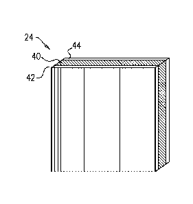
Device 24 comprises an electro-optical layer 40, such as a liquid-crystal
layer, which is
typically contained by suitable encapsulation, as is known in the art. Layer
40 has a local
effective index of refraction at any given location within its active area
(for example, within the
area of layer 40 that actually contains the liquid crystal) that is determined
by the voltage
applied across the layer at that location. The liquid crystal in layer 40 may
be birefringent, in
which case device 24 or system 20 may comprise a polarizer, as is known in the
art (omitted
from the figures for simplicity), in order to select the polarization of the
light that is to be
passed and refracted by layer 40. Alternatively, to avoid the need for a
polarizer, two such
lenses can be concatenated with perpendicular axes of birefringence, so that
each operates on a
different, orthogonal polarization, or a polarization-independent liquid
crystal layer, such as a
layer of cholesteric liquid crystal material, may be used.
12
CA 02884212 2015-03-05
WO 2014/049577 PCT/IB2013/058989
Transparent substrates 42 and 44, such as glass blanks, are positioned on
opposing sides
of layer 40, and respective electrodes are disposed on the substrates as shown
in Figs. 2B and
2C. The electrodes comprise a transparent, conductive material, such as indium
tin oxide
(ITO), as is known in the art. Alternatively, non-transparent electrodes may
be used, as long as
they are thin enough so that they do not cause disturbing optical effects. A
common electrode
50 on substrate 44 is positioned over the active area of layer 40 on one side.
Although this
common electrode is shown as a monolithic rectangle, it may alternatively have
any suitable
shape that sufficiently covers the active area of layer 40. An array of
excitation electrodes 46,
comprising parallel stripes of the transparent conductive material on
substrate 42, extends over
the active area on the opposite side of layer 40. (-Parallel" in this context
may include, as well,
electrodes that deviate in angle by several degrees.)
For example, the electrode patterns shown in the figures may be formed by
lithography
on substrates 42 and 44, after which the substrates are glued together at a
predefined distance,
typically a few microns, by using glues or etched spacers as are known in the
art. Layer 40 is
then inserted and sealed in the gap between the substrates. Although for the
sake of visual
clarity, only a few electrodes 46 are shown in Fig. 2C, in practice, for good
optical quality,
device 24 will typically comprise at least 100 stripe electrodes for
excitation, and possibly even
400 or more. This same proviso applies to the stripe electrodes shown in Figs.
3B and 3C.
Control circuitry 48 is coupled to apply respective control voltages to
excitation
electrodes 46, relative to the common voltage level of electrode 50. Control
circuitry 48
typically comprises amplifiers and/or switches, as are known in the art, which
control either the
amplitude or the duty cycle, or both, of the voltage that is applied to each
electrode 46. The
pattern of amplitudes and/or duty cycles applied to the electrodes determines
the phase
modulation profile of layer 40. The circuit components in circuitry 48 are
typically fabricated
as a silicon chip, which is then glued onto substrate 42, as shown in Fig. 2B.
Alternatively,
some or all of the components of circuitry 48 may be formed on a separate chip
and connected
to substrate 42 by suitable bonding wires or other connections. In either
case, the control
circuitry can be located at the side of the array of electrodes, as shown in
Fig. 3C, and there is
no need for any parts of the control circuitry to be located over the active
area of layer 40.
Circuitry 48 is able to modify the control voltages applied to each of a set
of the
excitation electrodes 46 (which may include all of the electrodes)
concurrently and
independently. For example, circuitry 48 may update the control voltages
applied to all the odd
electrodes in the array alternately with all the even electrodes. This sort of
approach scales
13
CA 02884212 2015-03-05
WO 2014/049577 PCT/IB2013/058989
readily to large electrode counts, and can thus be used to create electrically-
tunable optical
systems with high pixel counts and fine resolution.
As noted earlier. device 24 may be controlled in this manner to function as a
cylindrical
lens, with focal properties determined by the phase modulation profile induced
in layer 40 by
the voltages applied to electrodes 46. Optionally, these voltages may be set
so that device 24
functions as a cylindrical Fresnel lens. The control voltages applied to
excitation electrodes 46
may be modified so as to change the focal length of the cylindrical lens, as
well as to shift the
focal line of the cylindrical lens in a direction transverse to the device
(i.e., in a direction
parallel to the surface of substrates 42 and 44).
DEVICES WITH TWO-DIMENSIONAL PHASE MODULATION PROFILES
Figs. 3A-3D schematically illustrate an optical device 60 in which a two-
dimensional
phase modulation profile is created in a single electro-optical layer 62, in
accordance with
another embodiment of the present invention. Fig. 3A is a pictorial
illustration of device 60,
while Figs. 3B and 3C are side views showing transparent substrates 64 and 66
on opposing
sides of the device. Fig. 3D is a side view of device 60, showing a
superposition of excitation
electrodes 68 and 72 that are located on substrates 64 and 66 on the opposing
sides of the
device. Device 60 may be substituted into system 20 (Fig. 1), for example, in
place of the
combination of devices 24 and 26.
Device 60 contains an electro-optical layer 62, such as a liquid-crystal
layer, similar to
layer 40, as described above. Electrodes 68 and 72 on substrates 64 and 66,
respectively,
comprise parallel stripes of transparent conductive material extending over
the active area of
layer 62 in mutually-orthogonal directions. Although electrodes 68 and 72 are
of uniform
shape and spacing in the figures, the stripes may alternatively have varying
sizes and/or pitch.
Control circuitry 70 and 74, which may be of similar construction and design
to
circuitry 48 (Fig. 2B), applies control voltages to excitation electrodes 68
and 72, respectively.
As in device 24, the control circuitry in device 60 is able to modify the
control voltages applied
to each of a set of the excitation electrodes (which may include all of the
electrodes)
simultaneously and independently. Control circuitry 70 and 74 together,
however, can modify
the voltages applied to sets of the excitation electrodes on both of the sides
of layer 62, thereby
modifying the phase modulation profile of the layer in two dimensions.
Control voltages may thus be applied to excitation electrodes 68 and 72 so
that device
60 functions as a lens (possibly a Fresnel lens), having focal properties
determined by the phase
modulation profile. The control voltage waveforms result in a linear phase
response of the
14
CA 02884212 2015-03-05
WO 2014/049577 PCT/IB2013/058989
electro-optical layer, as defined and explained above. The control circuitry
can modify the
control voltages so as to change the focal length and/or to shift the optical
axis of the lens. The
voltage patterns applied by circuitry 70 and 74 across electrodes 68 and 72
may be chosen so as
to give a phase modulation profile that is circularly symmetrical, and may
thus emulate a
spherical lens. Alternatively, different voltage patterns may be applied so
that device 60
functions, for example, as an astigmatic lens, with a stronger cylindrical
component along one
axis or the other.
As shown in Fig. 3D, the superposition of electrodes 68 and 72 creates an
array of pixels
76, defined by the areas of overlap of the vertical stripes of electrodes 68
with the horizontal
stripes of electrodes 72. The center-to-center distance between the stripes
defines the pitch P of
the pixel array, while the width D of the conductive stripes themselves
defines the size of pixels
76. (Although these parameters are illustrated here with respect to the two-
dimensional array of
device 60, similar dimensions and considerations apply to the one-dimensional
arrays of
devices 24 and 26, described above.) These dimensional parameters of the
electrode array are
compared to the layer thickness T of electro-optical layer 62, shown in Fig.
3A.
In contrast to most liquid-crystal devices that are known in the art, the
inter-electrode
pitch P of device 60 is less than four times the thickness T of layer 62, and
may be less than
twice the thickness. Additionally or alternatively, the distance between the
electrode stripes (P-
D) may be less than the layer thickness T or possibly even less than one half
of T. In some
implementations, even the pitch P may be less than T. This choice of
dimensions permits a
high fill factor of pixels 76, and thus high resolution. Furthermore, the
relatively thick layer 62
enables device 60 to generate a large range of different phase shifts, while
the small pitch
supports modulation of the refractive index, and hence the phase shift, with
high resolution.
The crosstalk between adjacent pixels that results from this choice of
dimensions may actually
be beneficial in smoothing the phase modulation profile of the device, and
thus more closely
approximating the quadratic profile of a conventional lens.
As noted earlier, device 60, as well as the combination of devices 24 and 26
in system
20, can be used particularly to generate phase modulation profiles that are
separable in the X-
and Y-directions. The variation of the effective refractive index of a liquid
crystal or other
electro-optical layer, however, is generally not linear in the applied
voltage. In system 20, each
of devices 24 and 26 is controlled independently, so that the voltage applied
to electrodes 46 by
control circuitry 48 can be compensated to adjust for the nonlinearity. In
device 60, on the
other hand, the voltage across each pixel 76 is a function of the voltages
applied to both the
CA 02884212 2015-03-05
WO 2014/049577 PCT/IB2013/058989
vertical electrode 68 and the horizontal electrode 72 that cross at the pixel,
so that compensation
for nonlinearity is not straightforward.
In embodiments of the present invention, at least two different approaches may
be used
to achieve the desired linear phase response, and thus implement phase
modulation profiles that
are separable in the X- and Y-directions. One such approach is to limit the
range of applied
voltages, as described below with reference to Fig. 4. Alternatively, the
voltage waveforms
applied to electrodes 68 and 72 may be chosen so that their superposition
gives a linear
response in layer 62.
Fig. 4 is a schematic plot showing the dependence of the effective refractive
index n of a
liquid crystal layer in an optical device on the applied voltage V that is
used in controlling
device 60, in accordance with an embodiment of the present invention. (This
plot is based on
data presented by Wang et al., in -Liquid Crystal Blazed Grating Beam
Deflector," Applied
Optics 39. pages 6545-6555 (2000).) Although the curve shown is on the whole
nonlinear, it
has a roughly linear region in the approximate range of 1-2 V. referred to
herein as a quasi-
linear region. The term "quasi-linear" is used in the present description and
in the claims to
refer to a region in which the effective refractive index is approximately
linear in the voltage,
i.e.. n(V) = a + bV to within a predefined error bound, such as to within
10%, wherein a and b
are constant offset and slope parameters, respectively.
When voltages that form a cylindrical lens profile V(x) are applied to
vertical
electrodes 68 (n(x) = a + bVx(x) produces a cylindrical phase profile), and a
similar but
inverted profile V(y) = -V(y) is applied to horizontal electrodes 72, the
voltage profile across
layer 62 is V(x,y) = Vx(x) - Vy(y). This voltage profile gives a refractive
index profile:
n(x,y) = a + b[Vx(x) - Vy(y)] = a + bVx(x) - bVy(y),
so long as the voltages are in the linear (or quasi-linear) response region.
The first term (a) on
the right-hand side of the equation is constant and therefore does not
contribute to phase
modulation. The second and third terms are the horizontal and vertical
cylindrical lens
components, which together make up a two-dimensional lens.
Within the quasi-linear response region of layer 62, different phase
modulation values at
different pixels 76 can be obtained by either applying different voltages, or
applying the same
16
CA 02884212 2015-03-05
WO 2014/049577 PCT/IB2013/058989
voltages for different duty cycles, or a combination of both techniques, as
long as the refractive
index response is quasi-linear so that the equation n(x,y) = a + bVx(x) -
bVy(y) holds.
On the other hand, although limiting the applied voltages to the quasi-linear
range of
electro-optical layer 62 simplifies the operation of device 60, this
limitation is not essential.
Even when operating outside the quasi-linear range, the phase modulation of
layer 62 can be
expressed as the sum of the modulations applied over the X-axis and the Y-
axis. In this case,
control circuitry 70 and 74 may apply the control voltages to electrodes 68
and 72 as respective
waveforms, having respective temporal variation patterns chosen to generate a
set of specified
phase shifts in layer 62. If N different phase levels are required for a
Fresnel lens, for example,
then pairs of N different voltage waveforms for the X- and Y-directions
electrodes are chosen
in order to give the desired levels of phase response. Formally, voltage
waveforms are defined
for the X- and Y-direction electrodes, VXi (t) and Vyi (t) , i=0...N-1, such
that for each
i,j = 0...N-1, the phase response of layer 62 to the voltage difference
between the electrodes is
2Tr
ONXi (t) ¨ Vyi (t) = -I- 0+ j) ¨, wherein t represents time, and 00 is
the baseline phase.
The choice of appropriate waveforms permits any desired separable phase
profile to be
realized (within the limitations of the electro-optical layer). A method for
generating these
voltage waveforms is presented below in an Appendix. In the approach described
in the
Appendix, duty-cycle modulation is applied to the electrodes at a certain,
fixed voltage, but the
waveforms are chosen so that during certain (typically short) time periods,
the voltage across
the electro-optical layer is doubled due to overlap of the X- and Y-direction
waveforms. The
voltage effects are averaged by the liquid crystal, but not linearly, i.e., a
voltage V for a period
of 2T is not equivalent to a voltage of 2V for a period T. The latter will
have larger effect. This
added degree of freedom is used to solve the problem and choose appropriate
waveforms to
achieve the desired linear response.
It will be apparent based on this derivation, however, that this particular
choice of
waveforms is just one example of a possible implementation of this sort of
embodiment. Other
sets of waveforms may similarly be derived and are considered to be within the
scope of the
present invention.
It will thus be appreciated that the embodiments described above are cited by
way of
example, and that the present invention is not limited to what has been
particularly shown and
described hereinabove. Rather, the scope of the present invention includes
both combinations
17
CA 02884212 2015-03-05
WO 2014/049577 PCT/IB2013/058989
and subcombinations of the various features described hereinabove, as well as
variations and
modifications thereof which would occur to persons skilled in the art upon
reading the
foregoing description and which are not disclosed in the prior art.
APPENDIX - CONSTRUCTING VOLTAGE WAVEFORMS FOR PHASE RESPONSE
OF ELECTRO-OPTIC LAYER
PROBLEM STATEMENT:
Define voltage waveforms for X-direction and Y-direction electrodes
{17x,i (t)}N-01 and {17 0 y ,iN ¨ 1
such that for each k,1 = 0...N-1, the LC phase
i = i =
response to the voltage difference between the X- and Y-direction electrodes
is
TLC{VX,k VY ,1 (t)1 = ei(0 +(k+1)12N
DEFINITIONS
The following voltage waveform functions are defined for ¨T/4 < t < T/4. The
rest of
the function can be completed assuming the voltage functions are periodic and
alternating in
sign: V(t+T/2) = -V(t).
A step function with support between t1 and t2 is defined by : St1,t2 (V0, t)
=
fV0 ti < t < t2
0 otherwise'
t2¨ti
wherein D = ri./ is the duty cycle of St,,t2 (V0, t). The LC response depends
on the
2
duty cycle, and not on t1 and t2 separately.
A phase of a typical LC response to a step function, R(t2 ¨ t1, V0) =
T.Lc{Stl,t, t)} is:
1. Monotonically non-decreasing as a function of V0, and also concave as a
function of
V0.
2. Monotonically non-decreasing as a function of D, and also concave as a
function of D.
18
CA 02884212 2015-03-05
WO 2014/049577 PCT/IB2013/058989
By subtracting two step functions we can get a waveform that equals 2V0 , 170,
and 0
for different time regions. For example, for ti < t2 < t3:
2V0 ti < t < t2
St1,t3 (V0, t) ¨ St1,t2 (¨Vo, t) ¨= Vo t2 <t < t3.
1
0 otherwise
t 2 - t 1
This waveform has a duty cycle of Di = 7- at
voltage 2V0 , and D2 =
/2
t 3 - t 2
7 -/ at voltage V0. The LC response depends on the duty cycles Di and D2, and
not on
/2
t1, t2 and t3 separately.
CONSTRUCTING THE REQUIRED WAVEFORMS
Assumption: for each i, lix,i (t) =
Step 0: defining 17x,0 (t):
Step 0.0: the combination k=0, 1=0
a. Find Po for which R (po, V0) = e i 0 .
b. Define to = 7
vx,o(o= soo(voyo.
Thus, V0 (t) = S¨t0,0 (¨V
o, t).
Vxm (t) ¨ V,0 (t) = S_to,to NO , t) , and the response to V,0 (t) ¨
V17,0 (t), which is a step function of length po, is R (pop V0) = ei 0. Thus
these waveforms solve the problem statement for k=1=0.
19
CA 02884212 2015-03-05
WO 2014/049577 PCT/IB2013/058989
Step 1: defining Vx,i(t):
Step 1.0: the combination k=1, 1=0 (and also k=0, 1=1)
a. Find Pt for which R (pi, Vo) = ei( I
0 +N)
b. Define t1 = pi ¨ to
(t) = So,ti (Vo, t)
Thus, the response to Vx,i (t) ¨ Vy,0 (0, which is a step function of length
+1-E)
t1 + to = pi, is R (pi, Vo) = ei(0 N . and these waveforms solve the
problem statement for k=1 and 1=0 (and also k=0 and 1=1).
Step 1.1: the combination k=1, 1=1
The requirement is:
TLC{VX,1(t) VY,1 = ei(0 +212
0 N
a. Calculate the phase response 0 of TLC{Vx,1(t) ¨ Vy,i(t)}, for Vx,1 (t)
as defined in step 1Ø
b. If it is close enough (within the required tolerance) to the required value
(0 00
2Tr
¨), do nothing.
2 TE
c. If 0 is not close enough to the required value, then 0 < 00 + 2
. _ - (due to the
concave nature of R). In this case the pulse of length t1 is split into two
pulses of
lengths t1 ¨ X, and X respectively, in the form:
V,1 (t) So,ti_x t) S_to_x,_to t).
This form of waveform ensures that:
CA 02884212 2015-03-05
WO 2014/049577
PCT/IB2013/058989
a. The supports of Vx,1(t) and Vy (t) are disjoint, and thus LC response to
the combination k=1 and 1=0 does not change, since Vx,1 (t) ¨ Vy (t)
still equals 1/0 for a period of pi, and 0 otherwise.
b. Vx,i(t) ¨ Vy 1(0 equals 2V0 for a period of 2X. Since the LC
response to a voltage of 2V0 is stronger than the response to a voltage of VU,
increasing X will also increase the phase response, and a value X can be found
for which
0 To
TLCWX,1(t) VY,1 = ei(o +2'12
- =
Step n: defining Vx,n (t):
Step n.0: the combination k=n, 1=0 (and also k=0, 1=n)
= N
a. Find pn for which R (pn, = ei(0
b. Define tn = pn ¨ to
= So,tn Wo,
Thus, the response to Vx,n ¨ Vy (t) ,
which is a step function of length
tn to =pn, is R (pn, Vo) = ei(0.+n1i2N), and these waveforms solve
the problem statement for k=n and 1=0 (and also k=0 and 1=n).
Steps n.m, m=1 to n: the combinations k=n and 1=m:
The requirement is:
TLC{17X,n 17Y,m, = ei (0 n+m)
a. Calculate the phase response 0 of T Lc {V x ¨ Vy jn(t)}
21
CA 02884212 2015-03-05
WO 2014/049577 PCT/IB2013/058989
b. If it is close enough (within the required tolerance) to the required value
(0 ¨ o +
\ 2TE
(n + m) ¨), do nothing.
21T
c. If 0 is not close enough to the
required value, then 0 < (n + m) ¨
0
(due to the concave nature of R). In this case the pulse of Vx,n (0 is split:
A period
of X is deducted from the range [tn_1, til], and added to the range
[tim,¨t
This ensures that:
a. The LC response to the combinations k=n and 1=0..m-1 does not change.
h. The LC response to the combinations k=n and 1=m increases due to the added
¨217in
crease
the where Vx,n ¨ Vy,fli 0 . Increasing X will
the phase response, and a value X can be found for which
\zit\
(
TLC fl7X,71 (t) Vy,m, (t) = ei (0 +n+m)¨N)
22