Note : Les descriptions sont présentées dans la langue officielle dans laquelle elles ont été soumises.
CA 02885502 2015-03-13
WO 2013/175225 PCT/GB2013/051368
PRINTING OF LIQUID CRYSTAL DROPLET LASER RESONATORS ON A WET
POLYMER SOLUTION AND PRODUCT MADE THEREWITH
BACKGROUND TO THE INVENTION
Field of the invention
The present invention relates to methods for manufacturing photonic devices
and to
photonic devices manufactured by such methods. The invention has particular,
but not
exclusive, application to the manufacture of liquid crystal laser devices.
Related art
Liquid crystal (LC) materials are a class of functional photonic materials. LC
materials
contain molecules which have a tendency to self-organize along an optical
axis. The
way in which the molecules in LC materials align dictates the optical
properties of the LC
material, For example, chiral liquid crystals have a tendency to self-organize
into a
helicoidal arrangement around an optical axis. Due to the birefringence of the
material,
this helicoidal arrangement results in a periodic variation of the refractive
index along the
optical axis. For suitable periodicities, this gives rise to a photonic band-
gap for visible
wavelengths of circularly polarized light.
The optical properties of chiral LC materials make them suitable for
applications ranging
from bistable displays to lasers. Incorporation of an organic laser dye, as
the light
harvester or gain medium, into the optical cavity can lead to laser emission
at the
photonic band-edges. Laser devices built based on these materials are
characterised by
very low cost manufacturing, small size and selectable wavelength of emission,
currently
in the range 400 nm to 850 nm (See References [4] and [2]).
Applications of achiral LC materials include conventional flat-panel displays
(nematic
LCDs), variable retarders and SLMs.
US2011/0097557 discloses the manufacture of security features, e.g. for bank
notes, in
which a polymerisable LC material is printed onto a solid PVA layer. The PVA
layer is
unrubbed but is found to promote alignment for certain LC materials,
Conventional semiconductor lasers used in most modern laser systems are solid-
state
devices that are typically manufactured using a complex process involving a
combination
of deposition, etching and photolithographic steps on high quality single
crystal
1
CA 02885502 2015-03-13
WO 2013/175225 PCT/G B2013/051368
semiconductor wafers. Such conventional lasers cannot be manufactured using
relatively low cost printing technologies such as bar coating or inkjet
printing, for example.
It has previously been shown in References [11] and [12] that printable
emulsion-based
LC laser systems can be deposited on a wide variety of substrates including,
for
example, glass, plastic, metal or paper. These documents describe deposition
of a LC
lasing medium onto suitable substrates using emulsified samples and a simple
bar-
coating process. In these disclosures, the liquid crystal and laser dye
composition were
emulsified in a continuous phase of PVA, this emulsion then being applied to
the
substrate. Subsequent drying of, and interfacial interaction with, the
continuous phase
causes advantageous stresses to be applied to the LC droplets, assisting in
the
development of suitable alignment of the LC molecules.
SUMMARY OF THE INVENTION
The present inventors have found that although the approach described by
References
[11] and [12] provides a simple fabrication process, the approach has some
disadvantages. The individual LC droplets are polydisperse in terms of size,
typically
with diameters in the range of tens to hundreds of microns. This has an effect
on the
quality of the laser emission. Furthermore, the droplets are locally randomly
distributed
in the continuous phase. Therefore the approach used in References [11] and
[12] does
not allow accurate positioning of individual droplets, with the consequence
that the
spatial position of the ernission of light from the device cannot be
accurately controlled.
Accordingly, the present inventors attempted to overcome the above
disadvantages by
depositing patterns of LC lasing medium. The present inventors found that it
is indeed
possible to produce a required pattern of deposits of LC lasing medium, for
example by
inkjet printing. However, the present inventors have found that direct
deposition of the
LC lasing medium onto clean, dry surfaces fails to produce a suitable degree
of
alignment of the LC molecules (for example, a suitable alignment for many
devices that
use chiral LC materials is one in which the chiral LC helical axis is aligned
perpendicular
to the substrate).
Control of alignment within LC materials is known to be important to allow the
desired
optical properties of the LC material for a particular application to be
obtained. For
example, flat-panel display devices comprising nernatic LC require a uniform
direction of
2
CA 02885502 2015-03-13
WO 2013/175225
PCT/G B2013/051368
the LC director i.e. alignment of the LC material, for the display to
function. For example,
lack of uniform alignment within a deposited LC material for use as a lasing
medium can
result in multi-mode laser emission, or even no laser emissionõwhich is
typically
undesirable.
The present invention has been devised in order to address at least one of the
above
problems. Preferably, the present invention reduces, ameliorates, avoids or
overcomes
at least one of the above problems.
In a general aspect of the invention, the present inventors have found that it
is
advantageous to deposit a liquid crystal (LC) material onto a flowable layer
of material
that is substantially immiscible with the LC material. Furthermore, the
present inventors
have found that further advantages can be achieved when, on impact of the LC
material,
the flowable layer of material shapes the LC material with the result of
promoting
alignment of molecules in the LC material.
In a first preferred aspect, the present invention provides a method of
producing photonic
devices, such as lasers, or optical features by depositing liquid crystal (LC)
materials in
one or more discrete regions on surfaces.
In a second preferred aspect, the present invention provides a method of
manufacturing
a photonic device, the method comprising the steps of:
(i) providing an aliquot of a liquid crystal (LC) material of volume V,
volume V being
the same volume as that of a sphere of diameter DI; and
(ii) depositing the aliquot onto the surface of a flowable material layer
to form a liquid
crystal deposit, the flowable material and the LC material being substantially
immiscible,
wherein the liquid crystal deposit adopts a deformed shape relative to the
shape of the
aliquot due to interaction with the flowable material layer, the liquid
crystal deposit having
a maximum length Ll, measured in a direction parallel to the flowable material
layer
surface before deposition, wherein L1 is greater than D1.
In a third preferred aspect, the present invention provides a photonic device
obtained by
or obtainable by the method of the first or second aspect.
3
CA 02885502 2015-03-13
WO 2013/175225
PCT/G B2013/051368
In a fourth preferred aspect, the present invention provides a laser device
obtained by or
obtainable by the method of the first or second aspect.
In a fifth preferred aspect, the present invention provides a photonic device
having at
least one liquid crystal (LC) material deposit formed on an underlayer, the
underlayer
having an underlayer surface surrounding the LC material deposit, wherein the
liquid
crystal deposit has a maximum length L2, measured in a direction parallel to
the
underlayer surface surrounding the LC material deposit, and a maximum height
H2,
measured in a direction perpendicular to the underlayer surface surrounding
the LC
material deposit, so that L2 is greater than H2, wherein the liquid crystal
deposit is
shaped to project above the underlayer surface surrounding the LC material
deposit.
In a sixth preferred aspect, the present invention provides a use of a
photonic device
according to the third or fifth aspect, in which the photonic device is
subjected to
illumination by a source of electromagnetic radiation and provides a
corresponding
response which is detected by a detector or by observation.
Any of the aspects of the invention may be combined with each other.
Any of the aspects of the invention may have any one or, to the extent that
they are
compatible, any combination of the following optional features.
The term liquid crystal (LC) material as used herein describes a material
containing at
least 50 wt.%, preferably at least 75 wt. ck, more preferably at least 90 wt.%
of at least
one chemical compound that exhibits liquid crystalline behaviour. Optionally
the LC
material contains a plurality of chemical compounds known to exhibit liquid
crystalline
behaviour. Preferably the LC material contains elongated molecules.
Suitably the LC material is a chiral LC material, that is a material
containing at least 50
wt.%, preferably at least 75 wt.%, more preferably at least 90 wt.% of at
least one
chemical compound that exhibits liquid crystalline behaviour and a chiral
additive, for
example BDH-1281. The addition of a chiral additive allows the chirality of
the LC
material to be controlled by controlling the periodicity of the variation in
refractive index in
the LC material. Suitable chiral additives are described in US Patent 6217792
and
WO 2011/137986. Suitably the chiral LC material contains less than 10 wt.% of
chrial
4
CA 02885502 2015-03-13
WO 2013/175225 PCT/G B2013/051368
additive. Preferably the chiral LC material contains about 2 wt.% to 6 wt.% of
chiral
additive. Chiral LC materials have a tendency to align in a helicoidal
arrangement.
Chiral LC materials are particularly suitably for the formation of a band-edge
laser.
Alternatively the chiral LC material contains a chiral chemical compound known
to exhibit
liquid crystalline behaviour.
The LC material may be one, or more, of nematic, chiral nematic, smectic or
blue phase
materials. Chiral nematic materials are particularly preferred.
Suitably the LC materials form a laser. Preferably the LC material exhibits
photonic
band-edge lasing. Alternatively the LC material may exhibit random lasing.
Optionally the LC material includes a fluorescence dye, a fluorescent laser
dye, a
quantum dot, or other light harvester or gain additives, such as Nd:YAG,
Ti:sapphire,
Cr:sapphire Cr:LiSAF Er:YLF, Nd:glass, and Er:glass. to allow the LC material
to
function as a lasing medium.
Suitably the LC material exhibits a nematic phase. A chiral LC material
exhibiting a
nematic phase is particularly suitable for the formation of a band-edge laser.
However,
these materials may also be used to form a random laser.
Optionally the LC rnaterial exhibits a smectic phase. Chiral smectic LC
materials are
suitable for the formation of a band-edge laser and may also be used to form a
random
laser.
Optionally the LC material exhibits a blue phase II or III. Blue phase
materials are
particularly suitable for the formation of a band-edge laser.
In alternative embodiments, it is not necessary for the LC material to form a
laser. This is
the case where, for example, it is intended that the photonic device is a
passive device.
Suitable passive devices include, for example, Bragg-like reflectors, where a
known
portion of the electromagnetic spectrum is selectively reflected over other
regions of the
spectrum.
5
CA 02885502 2015-03-13
WO 2013/175225
PCT/G B2013/051368
Preferably the aliquot of liquid crystal material is provided by inkjet
printing. To overcome
the problem of providing accurate spatial positioning, the present inventors
have
developed an inkjet-based process which can preferably be used to construct
arrays of
LC lasers or other photonic devices whilst preserving the desirable emission
characteristics.
The method of the present invention may be used to construct patterned arrays
of liquid
crystal material deposits, for example a pre-designed complex two dimensional
pattern.
The patterned array may also be a regular array of liquid crystal deposits.
The photonic device of the present invention may have a plurality of liquid
crystal
deposits in a regular and/or patterned array.
Optionally the liquid crystal deposit is shaped to project above and below the
flowable
material layer (or underlayer surface) surrounding the LC material deposit.
Optionally the flowable material layer at least partially encapsulates the LC
deposit.
Where, for example, the LC deposit adopts a lenticular shape, the flowable
material layer
may encapsulate one of the major convex surfaces of the lenticular shape.
The additional advantage of using an inkjet process is the flexibility in not
only depositing
the laser rnaterials themselves, with controllable emission characteristics,
but that further
additive processing is made significantly easier. Thus, for example, further
materials can
be deposited via inkjet printing. The flowable material layer may be deposited
via inkjet
printing (before deposition of the LC material). Other materials may also be
deposited in
this way, such as other polymeric layers to assist with or provide protection
of the LC
material and/or improve alignment within the LC material.
The length L1 of the liquid crystal deposit is the maximum distance across the
liquid
crystal deposit on the flowable material layer, measured along a straight line
parallel to
the flowable material layer surface. For example, when the liquid crystal
deposit is a
substantially circular island when viewed in plan view, L1 is the diameter of
the island.
The liquid crystal deposit has a minimum width W1. The width W1 of the liquid
crystal
deposit is the minimum distance across the liquid crystal deposit on the
flowable material
6
CA 02885502 2015-03-13
WO 2013/175225
PCT/G B2013/051368
layer, measured along a straight line parallel to the flowable surface and
passing through
the centre point (or centroid) of the liquid crystal deposit when viewed in
plan view. Here,
the surface of the flowable material layer is considered before deposit of the
LC material
deposit. For example, when the liquid crystal deposit is a substantially
circular island
when viewed in plan view. W1 is the diameter of the island.
The width \N2 of the liquid crystal deposit is the minimum distance across the
liquid
crystal deposit on the support layer (or underlayer), measured parallel to the
support
layer surface (or the underlayer surface) surrounding the LC deposit, in a
similar manner
to W1. W2 may be different to W1 due to a transformation of the flowable
material layer
to the support layer (or underlayer).
The length L2 of the liquid crystal deposit is the maximum distance across the
liquid
crystal deposit on the support layer (or the underlayer), measured parallel to
the support
layer surface (or the underlayer surface) surrounding the LC deposit. For
example, when
the liquid crystal deposit is a substantially circular drop. L2 is the
diameter of the drop.
L2 may be different to L1 due to a transformation of the flowable material
layer to the
support layer (or underlayer).
The length L1 can be measured via static image microscopy after deposition of
the
deposit. The length L2 can be measured via static image microscopy after the
step of
transforming the flowable material layer into the support layer.
The width W1 can be measured via static image microscopy after deposition of
the
deposit. The width W2 can be measured via static image microscopy after the
step of
transforming the flowable material layer into the support layer.
The diameter al can also be measured via microscopy. In the case of inkjet
printing, D1
can be measured via video microscopy by capturing images of the generated drop
after
generation from an inkjet nozzle but before deposition at the flowable
material layer.
Alternatively, for other deposition processes, D1 can be calculated based on
knowledge
of the volume V of the aliquot of LC material.
The height H1 of the LC material deposit is the maximum height of the liquid
crystal
deposit measured perpendicular to the flowable material layer surface. Here,
the surface
7
CA 02885502 2015-03-13
WO 2013/175225
PCT/G B2013/051368
of the flowable material layer is again considered before deposit of the LC
rnaterial
deposit.
The height H2 of the liquid crystal deposit is the maximum height of the LC
material
deposit measured perpendicular to the support layer surface (or the underlayer
surface)
surrounding the LC material deposit.
The height H1 and H2 of the liquid crystal deposit can also be measured via
static image
microscopy after deposition of the drop. The height H1 and H2 can also be
measured
using SEM.
To overcome the problem of poor alignment within the LC material, the present
inventors
have developed an approach taking advantage of the fact that certain flowable
materials
can be identified and selected in which the LC materials are not substantially
miscible.
For example suitable LC materials tend not to be miscible in polymer solutions
such as
aqueous PVA. This is demonstrated in References [9], [11] and [12], in which
an
emulsion of the LC material phase in a continuous phase of aqueous PVA is
formed.
The present inventors have found that when the droplets of the LC phase are
smaller in
volume than the flowable material, e.g. the polymer solution, as in the case
of small
deposits on a flowable material layer, e.g. a wet film, the interfacial
tension stresses and
distorts the LC phases (deposits). The effect of this is to promote the
desired alignment
of the LC molecules in the liquid crystal deposit.
The present inventors have found that inkjet printing of a LC material allows
for accurate
spatial positioning of the LC material on the surface on which it is printed.
Inkjet printing
of a LC material onto a flowable rnaterial that is substantially immiscible
with the LC
material improves the spatial positioning of LC material on the surface and
also improves
alignment within the LC material. The substantial immiscibility of the two
materials
means that the materials form distinctive phases when placed in contact with
one
another. Where the LC material deposit has a circular shape in plan view, the
interfacial
tension between the LC material and the flowable material layer shapes the
deposit of
the LC material to have a diameter D2 which is greater than the diameter D1 of
a sphere
with the same volume V as the aliquot of LC material deposited. This
distortion induces
alignrnent of molecules within the LC material. The non-contact and "self-
assembly"
nature of this method allows for low-cost and flexible manufacturing of
photonic devices
8
CA 02885502 2015-03-13
WO 2013/175225
PCT/G B2013/051368
on a broad range of surfaces. This method also allows for precise control of
patterning
along with control over the photonic property of the LC material by inducing
alignment in
the LC material.
Suitably the volume of flowable material in the flowable material layer is
greater than the
volume of LC material deposited by inkjet printing in the process of the
present invention.
Preferably, the depth of the flowable material layer (or underlayer) is
greater than the
maximum height H1 and/or H2 of the LC material deposit. More preferably, the
depth of
the flowable material layer (or underlayer) is greater than the diameter D1 of
a sphere
with the same volume V as the aliquot of LC material.
Preferably H2 is greater than 1 .m; preferably greater than 5 m. Preferably
H2 is less
than 100 m. Preferably H2 is in the range 1 !Am to 100 m; more preferably 5
m to
50 pm and most preferably in the range 5 pm to 30 m.
Preferably the ratio of H1 to H2 is not less than 1:1.
Preferably the ratio of H1 to H2 is not more than 50:1.
A deposit of LC material having H2 within the values described above is
considered to be
particularly suitable for use as a laser due to the resultant length of lasing
cavity.
Preferably the ratio D1 to H1 is less than 50:1.
Preferably the ratio of L2 to H2 is from 2:1 to 200:1.
Preferably, the ratio of L1 to al is not more than 20:1, preferably less than
10:1, and
most preferably less than 3:1.
Preferably, the ratio of L1 to H1 is not less than 1:1.
Preferably, the ratio of Ll to H1 is not more than 50:1.
Preferably, the ratio of L2 to H2 is not less than 1.1:1
9
CA 02885502 2015-03-13
WO 2013/175225
PCT/G B2013/051368
Preferably, the ratio of L2 to H2 is not more than 1000:1.
Preferably the ratio of W1 to D1 is not less than 0.1:1.
Preferably the ratio of W1 to D1 is not more than 20:1
Preferably the ratio of W1 to W2 is not more than 1:1.
Preferably the ratio of W1 to W2 is not less than 0.01:1.
Preferably the ratio of L1 to W1 is not less than 1:1.
Preferably the ratio of L1 to W1 is not more than 200:1.
Preferably the ratio of L2 to W2 is not less than 1:1.
Preferably the ratio of L2 to W2 is not more than 1000:1.
The present inventors have found that operating within the ranges identified
above tends
to promote alignment of the LC material in the LC material deposit, due to
shaping
effects caused by interaction with the flowable material layer.
In some embodiments, LC materials are deposited by inkjet printing onto a
liquid layer.
The liquid layer here is an example of the flowable material layer of the
second aspect of
the invention.
In some embodiments, the liquid layer is deposited by film coating using a
doctor blade,
or bar coating, or roll-coating or inkjet deposition of either a continuous
wet film (e.g.
solution layer), individual drops, groups of connected drops, or multiple
drops in the
same location.
Suitably the method comprises a step of transforming the flowable material
layer into a
support layer. Typically, this takes place after deposition of the LC material
drop.
Optionally the step of transforming the flowable material layer includes
curing the
flowable material layer to form a support layer. The step of transforming the
flowable
CA 02885502 2015-03-13
WO 2013/175225
PCT/G B2013/051368
material layer into a support layer may involve any chemical or physical
process which
may convert, e.g. a liquid, into a solid or a semi-solid. Optionally the step
of transforming
the flowable material layer involves cooling (e.g. solidification), solvent
evaporation,
cross-linking, or polymerization (such as photo induced polymerization) of the
flowable
material layer. VsVhen the flowable material is a solution, transforrnation
into the support
layer may involve evaporation of some or all of the solvent from the solution.
The
transformation of the flowable material layer into a support layer provides
the advantage
that the LC material can be supported at a desired location within the support
layer.
Therefore, the support layer preferably prevents movement of the LC material
drop from
the desired location, e.g. during movement or vibration of the photonic
device.
The step of transforming the flowable material layer into a support layer may
also involve
shrinking the flowable rnaterial layer. For example, when the flowable
material is a
solution, evaporation of the solvent to form the support layer may also result
in shrinking
of the flowable material layer. Shrinking of the flowable material may further
distort the
drop of the LC material to further improve alignment of molecules within the
LC material.
The step of transforming the flowable material layer into a support layer may
also involve
distorting the LC material deposit. The maximum length of the LC material
deposit after
the step of transforming the flowable material layer into the support layer is
L2. The
maximum height of the LC material deposit after the step of transforming the
flowable
material layer into the support layer is H2.
In some embodiments the maximum length of the LC material deposit increases
during
the transformation of the flowable material layer into the support layer such
that L2 is
greater than L1. This further improves alignrnent within the LC rnaterial.
In some embodiments the maximum height of the LC material deposit decreases
during
the transformation of the flowable material layer into the support layer such
that H2 is
less than H1. This further improves alignment within the LC material.
Optionally, after the transformation of the flowable material layer into a
support layer, the
ratio of the maximum length L2 of the LC material deposit on the support layer
to the
diameter D1 of the sphere having the same volume V as the aliquot of LC
material is
11
CA 02885502 2015-03-13
WO 2013/175225
PCT/G B2013/051368
preferably less than 20:1, more preferably less than 10:1, and most preferably
less than
3:1.
Suitably the method comprises the step of curing the LC material deposit. The
step of
curing the LC material rnay include photopolyrnerization of reactive monomers,
for
example when liquid crystalline mono- and di-acrylate materials are contained
in the LC
material or where the LC material itself is polymerizable. Curing the
deposited drop of
LC material prevents disruption of the improved alignment achieved by the
method of the
present invention, e.g. during movement or vibration of the photonic device.
Suitably the flowable material is a liquid. Preferably the liquid is a
solution, for example a
polymer solution. The liquid may be a colloidal solution, suspension or
emulsion. In
some embodiments the flowable material layer is a polymer-dispersed liquid
crystal layer
as described in References [11] and [12]. In other embodiments, the flowable
material
may be a material which deforms plastically in response to the arrival of the
generated
drop, e.g. a gel or a paste.
When the flowable material is a polymer solution, the polymer solution may
comprise a
polymer selected from the group including: PVA; polyurethane; polyamides, e.g.
Nylon
6,6; PMMA: polyimides, poly(pyromellitic dianhydride oxydianilines) and
polystyrene.
The solvent may be any suitable solvent, for example: water, dichloromethane,
formic
acid, acetone, iso-propyl alcohol, toluene, cyclohexane or other organic
solvents or
derivatives, for example.
Optionally the polymer solution has a concentration from 1 wt % to 30 wt %.
More
preferably the polymer solution has a concentration frorn 5 wt % to 20 wt
,10.
In some embodiments the flowable material comprises a lasing material, for
example the
flowable material may be an emulsion based lasing medium as described in
References
[11] and [12]. When the LC rnaterial deposit comprises a lasing material, the
flowable
material may exhibit the same lasing action as the LC material deposit.
Alternatively the
flowable material may exhibit lasing action of a different type to the LC
material deposit.
Preferably the flowable material contains an alignment component to promote
alignment
in the LC material. The alignment component may include polyimides,
surfactants,
12
CA 02885502 2015-03-13
WO 2013/175225
PCT/G B2013/051368
polymers (e.g. polyvinyl alcohol, polyurethane, polyamides, Nylon 6,6,
polymethyl
methacrylate or poly(pyromellitic, polydiandydride oxydianiline)) or
derivatives of these
materials which promote a preferred orientation of the LC.
The flowable material containing an alignment component provides the advantage
of
providing chemical control of alignment within the LC material in addition to
the physical
control by shaping the LC material deposit. Therefore the use of an alignment
component further improves alignment within the LC material.
Preferably the flowable material contains an alignment component to promote
planar
degenerate alignment in the LC material. When the LC material is a chiral LC
material,
suitably the planar degenerate alignment component causes homeotropic
alignment
(perpendicular anchoring) of the LC optical axes within the LC material
deposit.
The use of a planar degenerate alignment component also further improves
alignment
within the LC material. For example, a chiral LC material contains molecules
which self-
organise along a helicoidal axis, as discussed above. The shaping of the LC
material
deposit described above improves the alignment of the helicoidal axes.
Providing a
planar degenerate alignment component in the flowable material layer causes
molecules
at the base of the LC material deposit to align parallel to the surface of the
flowable
material layer. This alignment of molecules at the base of the helicoidal
structures
causes the helicoidal axes to align perpendicular to the flowable material
layer surface
(or underlayer surface). This is particularly advantageous for band-edge
lasing.
Suitably, the flowable material layer is formed on a substrate. Another
advantage of the
present invention is that the choice of substrate is not particularly limited.
The substrate
may be any material onto whose surface the flowable material may be deposited
and
which provides a suitable support for the photonic device. The substrate may
be light-
transmissive or reflective, e.g. to allow illumination of the LC material drop
with pumping
radiation for operation as a laser. Therefore suitable substrates include
light-
transmissive glass and light-transmissive plastics. The substrate may, for
example, be
rigid or substantially rigid. Alternatively, the substrate may be flexible.
13
CA 02885502 2015-03-13
WO 2013/175225
PCT/G B2013/051368
The surface of the substrate may be patterned with structures, such as wells
or barriers.
The patterned substrate allows further control of the spatial location, or
shape of the
flowable layer, deposited LC material and/or protective layers.
Preferably the flowable material layer is deposited by film coating using a
doctor blade,
bar coating, roll-coating or inkjet deposition of a continuous film,
individual drops, or
groups of connected drops. Inkjet deposition of the flowable material allows
continuous
"printing" of LC photonic devices.
Alternatively, the flowable material may be deposited in discrete regions, for
example, in
the form of either individual deposits or groups of connected deposits to form
lines or
other features. The provision of discrete regions of flowable material layer
allows
asymmetric stress to be induced in the later deposited LC materials to produce
desired
optical features.
When inkjet printing is used to deposit the flowable material, the digital
nature of the
inkjet deposition method also allows flexibility of altering the order and
location of
material deposition, e.g. LC materials onto flowable material or vice versa,
or creating
multi-layer structures consisting of one or more layers of LC materials and
other flowable
materials. The application of the method of the present invention described
can also
extend to a wider range of LC materials, including but not limited to nematic,
chiral
nematic, smectic, blue phase or any combination of these materials.
Suitably, the method comprises a step of providing a protective layer.
Preferably, the
protective material layer is deposited on top of the LC material deposit. The
protective
material may be the same material as the flowable material. The protective
material
layer may be transformed into a protective support layer. Preferably the
protective
material layer and the flowable material layer (or support layer, or
underlayer) together
totally encapsulate the LC material deposit. The protective material layer may
also
further shape the LC material deposit to induce further alignment within the
LC material.
The protective material layer may provide a hydrophobic or hydrophilic
surface. The
protective material layer may be an oxygen scavenger or getter. The protective
material
layer may be a moisture barrier or a preferential absorber. For example,
polyurethane,
PVA, polydimethylsiloxane or other silicones may be used. The optional and
preferred
14
CA 02885502 2015-03-13
WO 2013/175225 PCT/G B2013/051368
features described above for the flowable material layer also apply to the
protective
material layer. For example, preferably the protective layer contains an
alignment
component to improve alignment in the LC material deposit. Suitably protective
materials may comprise: PVA , polyurethane; Nylon 6,6, polymethyl
methacrylate,
polyimides, poly(pyromellitic dianhydride oxydianiline), metal-oxide polymer
composites
or derivatives of these materials.
As mentioned above; preferably the flowable material layer has a thickness T1
greater
than diameter D1 that would be attributed to the volume V of the LC material
aliquot.
This allows the flowable material layer to shape the deposit of LC material.
Preferably the flowable material has a thickness T1 less than 10 times the
diameter D1 of
the generated drop of LC material. Suitably the thickness T1 is between 10 mm
and 10
nm, more suitably between 1 mm and 1 pm, and more suitably still between 100
pm and
10 pm. If T1 is too large the drop of LC material deposited on the flowable
material layer
may be moved from the location of deposition by currents caused within the
flowable
material. For example, when the flowable material is a solution, the length of
time the
flowable material exists in a liquid phase is typically increased as the
thickness of the
flowable material layer is increased. As the solvent evaporates from the
solution layer
this may cause a current to flow in the flowable material which may disturb
the position of
a drop of LC material on the flowable material layer. Therefore control of the
thickness of
the flowable material layer is advantageous. Control of the curing rate of the
flowable
material layer is also advantageous for the same reasons.
Preferably the ratio of the thickness T2 of the support layer to the thickness
of the
flowable layer is in the range 1:1 to 0.01:1.
Preferably the flowable material layer has a substantially constant thickness
across the
layer. Inkjet printing of the flowable material layer allows precise control
of the thickness
of this layer.
Suitably the protective layer has a thickness in the range of 10nm to lOmm.
Preferably the method comprises providing a second, and optionally a third,
and
optionally a fourth etc., aliquot of a LC material and depositing it on a
flowable material
CA 02885502 2015-03-13
WO 2013/175225
PCT/G B2013/051368
layer, i.e. steps (i) and (ii) are repeated. In this way, there can be
provided a device
having a plurality of photonic locations such as active photonic locations.
Suitably the
second and optionally further deposits of LC material are deposited on the
same flowable
material layer as the first drop but each in a different location from the
first drop. In this
way the method may be used to obtain an array (preferably an ordered array) of
LC
material deposits on the flowable material layer. Alternatively the second,
and optionally
third, and optionally fourth etc., deposits may each be deposited on a
different flowable
material layer, i.e. a second, and optionally third, and optionally fourth
etc., flowable
material layer. In this way the method may be used to obtain LC material
deposits on
several separate flowable material layers. In this case, the flowable material
layers may
be different, e.g. in terms of composition, thickness etc. in order to provide
different
control to the drops of LC material.
In some embodiments the method comprises generating a second, and optionally a
third,
and optionally and fourth etc., aliquot of a LC material and depositing the LC
material on
a flowable material layer in the same location as the first LC material
deposit. This
allows the size of the LC material deposits to be controlled.
In some embodiments, when a plurality of aliquots of LC material are provided,
the LC
material deposited in different locations may be the same LC material.
Alternatively the
LC material deposited in different locations may be different LC materials,
for example
when different lasing action is required at different locations.
Preferably the ratio of the volume V (measured in 4m3) of the aliquot of LC
material to the
length L1 (measured in jim) of the LC material deposit is in the range 10:1 to
1,000,000:1
In some embodiments, it is preferred that the flowable material layer
comprises two or
more distinct layers. This can be advantageous in order to provide an upper
layer that
provides a specific desired interaction with the incoming LC aliquot and a
lower layer (or
lower layers) that provides either a desired interaction with the incoming LC
aliquot or
another a desired interaction with the upper layer.
In a sixth preferred aspect, the present invention provides a use of a
photonic device
according to the third or fifth aspect, in which the photonic device is
subjected to
16
CA 02885502 2015-03-13
WO 2013/175225
PCT/G B2013/051368
illumination by a source of electromagnetic radiation and provides a
corresponding
response which is detected by a detector or by observation.
In relation to the sixth aspect of the invention, there are several modes of
operation of the
photonic device which are contemplated. These depend on the device itself and
on the
illumination of the device.
Where the photonic device is a laser, the device typically incorporates a
laser dye. The
illumination by a source of electromagnetic radiation preferably provides
optical pumping.
In this case the source is itself typically a laser. However, the source may
alternatively
be an LED such as a high power LED.
It is possible to operate the laser above threshold. That is, the optical
pumping provided
by the source is sufficient to provide lasing in the LC material deposit.
However, it is alternatively possible to operate the laser below threshold, by
suitable
adjustment of the power of the source, the output spectrum of the source, or
by using a
different source. In this case, the laser dye may still fluoresce, but the
number of
photons emitted by the laser dye is insufficient to cause true lasing.
However, the optical
output of the device may include characteristics related to the interaction of
the photons
emitted by the laser dye and the photonic band gap of the LC material deposit.
In this
case, therefore, below-threshold operation of the photonic device may be
suitable to
provide a characteristic output that can be detected or observed. In this
manner, below-
threshold operation of the photonic device may provide a security feature that
can be
interrogated using a suitable illumination source. Furthermore, other
fluorescent
chrornophores may be used in place of a conventional laser dye. These may
include
other fluorescent taggants, dyes or quantum dots, for example, where the
native
fluorescence is modified by the presence of the liquid crystal photonic
bandgap.
It is of particular interest to note that the same photonic device can be
subjected to either
of the modes of operation mentioned above. Thus, where a suitable source of
electromagnetic radiation is available, the photonic device can be operated
above
threshold, with the resultant and the laser output from the device. However,
where only a
lower power source of electromagnetic radiation is available, the photonic
device can be
operated below threshold, with the resultant below-threshold characteristic
output.
17
CA 02885502 2015-03-13
WO 2013/175225 PCT/G B2013/051368
The photonic device need not incorporate a laser or fluorescent dye. The
photonic
device may be used in passive mode. In this case illumination of the device by
ambient
light or by light from a particular source (e.g. an LED of known spectral
output) can cause
selective reflection from the photonic device based on the photonic bandgap.
Non-
fluorescent dyes, or material which absorbs certain portions of the
electromagnetic
spectrum, may also be added to the mixture to create a characteristic
signature.
In each of these modes of operation, it is preferred that multiple photonic
devices are
provided, arranged in a suitable array or pattern. The array or pattern may be
ordered,
e.g. it may have some degree of symmetry or provide a recognisable shape.
However, it
is not essential that the array or pattern is ordered. A truly random or an
apparently
random array or pattern can be used. The positional location of the devices on
the
substrate and relative to each other can be used to encode information. Such
arrays or
patterns are straightforward to achieve based on the inkjet printing approach
described.
The optical response may vary from device to device in the array. The
resultant arrayed
optical response of the photonic devices, when suitably illuminated, provides
a powerful
basis for a security feature for identifying objects or documents of value.
Further optional features of the invention are set out below.
BRIEF DESCRIPTION OF THE DRAWINGS
Embodiments of the invention will now be described by way of example with
reference to
the accompanying drawings in which:
Fig. 1 shows the emission spectrum under optical excitation at a wavelength of
532nm
for a deposit of comparative example 'I;
Fig. 2 is a schematic view showing the creation of the flowable material layer
according
to an embodiment of the present invention;
Fig. 3a is a schematic view showing inkjet printing of a LC material according
to an
embodiment of the present invention;
18
CA 02885502 2015-03-13
WO 2013/175225
PCT/G B2013/051368
Fig. 3b is an enlarged view captured during microscopic imaging of the print
head shown
in Fig. 3a at 0 ps during generation of a deposit of LC material;
Fig. 3c is an enlarged view captured during microscopic imaging of the print
head shown
in Fig. 3a at 20 ps during generation of a deposit of LC material;
Fig. 3d is an enlarged view captured during microscopic imaging of the print
head shown
in Fig. 3a at 50 ps during generation of a deposit of LC material;
Fig. 3e is an enlarged view captured during microscopic imaging of the print
head shown
in Fig. 3a at 250 ps during generation of a deposit of LC material;
Fig. 4a is a scaled high-speed microscopic image showing the deposit of LC
material
generated by an inkjet printing head at a reference time of 0 ms;
Fig. 4b is a scaled high-speed microscopic image showing the deposit of LC
material
impacting the surface of the flowable material layer 0.2 ms after the
reference time;
Fig. 4c is a scaled high-speed microscopic image showing the deposit of LC
material on
the flowable material layer 0.6 ms after the reference time;
Fig. 4d is a scaled high-speed microscopic image showing the deposit of LC
material on
the flowable material layer 100 ms after the reference time;
Fig. 4e is a scaled high-speed microscopic image showing the deposit of LC
material on
the flowable material layer 500 ms after the reference time;
Fig. 4f is a scaled high-speed microscopic image showing the deposit of LC
material on
the flowable material layer 2 s after the reference time;
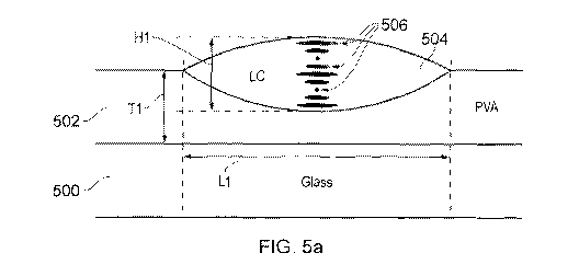
Fig. 5a is a schematic cross-section showing the deposit of LC material on the
flowable
material layer;
Fig 5b is a schernatic plan view showing the deposit of LC material on the
flowable
material layer;
19
CA 02885502 2015-03-13
WO 2013/175225
PCT/G B2013/051368
Fig. 6 is a graph showing the laser emission following optical excitation at
the absorption
maximum of the laser dye from a deposit of LC material deposited according to
the
present invention; and
Fig. 7 is a graph showing output intensity as a function of excitation energy
for the same
LC material as Fig. 6.
Fig. 8 is a graph showing an example reflection band for a chiral nematic LC
material and
for the same chiral nematic LC material combined with a dye.
Fig. 9 shows the spectral response for the sample of Example 5.
Fig. 10 shows the spectral response for the sample of Example 6.
DETAILED DESCRIPTION OF THE PREFERRED EMBODIMENTS, AND FURTHER
OPTIONAL FEATURES OF THE INVENTION
Chiral nematic liquid crystals (LCs) are a unique class of functional photonic
materials
with applications ranging from bistable displays to lasers.(11[2) In these
materials, the
constituent elongated molecules self-organize into a helicoidal arrangement
around the
helical, or optical, axis. The resultant periodic variation of the refractive
index gives rise to
a photonic band-gap for visible wavelengthsPIThis has recently received
significant
interest in the context of photonic band-edge lasing, [2. 4] since
incorporation of an organic
fluorescent dye, as the gain medium, into the helical structure, or optical
cavity, can lead
to laser emission at the photonic band-edges. Such systems offer high slope
efficiency,
greater than 60%, narrow linewidth emission [5] and, with the self-organized -
soft"
periodic structure, broadband wavelength selectivity and tuneability. Typical
laser
emission wavelengths are in the range 450 nm to 850nm16-101. The present
invention
exploits the liquid-like properties of the chiral LC laser and describes an
inkjet deposition
approach for these materials. Such an approach allows simple and arbitrary
positional
control of laser sources, incompatible with conventional laser processing and
fabrication,
to realize new classes of functional photonic materials and devices.
CA 02885502 2015-03-13
WO 2013/175225
PCT/G B2013/051368
Lasing LC media offers significant potential for not only reducing
manufacturing cost, but
also to form coatings on surfaces, or devices, currently inaccessible to the
traditional
processing required in the fabrication of semiconductor lasers. Precise and
controllable
positioning of the location and size of individual laser deposits would
significantly improve
the functionality of the laser coatings and devices. Ordered laser array
structures, for
example, would be of particular interest in bio-assay arrays, optofluidic
applications and
new information displays.
In recent years, there has been increased interest in using direct writing
processes such
as inkjet printing as flexible fabrication methods for electronics and
biological devices. [141
The present invention uses a "drop-on-demand" [15 inkjet deposition process
that controls
precisely the aliquot size and allows the formation of spatially localized
arrays of LC
material deposits, for example spatially localized laser sources. By
depositing the LC
lasing material onto a flowable material, e.g. a wet, solution-based polymer,
the
necessary alignment within the LC material can be obtained.
When the LC material contains a laser dye, following optical excitation at the
absorption
maximum of the laser dye, single-mode laser emission is observed with a well
defined
threshold and narrow linewidth when the necessary alignment within the LC
material is
obtained. The present invention shows that the inkjet deposition process has
only a
minor effect on the lasing threshold and emission characteristics of the LC
laser system
relative to control cells fabricated using conventional glass cell assembly
methods. The
results demonstrate the possibility of creating truly two-dimensional laser
arrays of
controlled and arbitrary size, position, and wavelength for use in a diverse
range of
applications.
Although a central aim of the development of the present invention has been to
manufacture laser devices, it is not essential that the final device is a
laser device. Other
photonic devices are contemplated. Other optical effects can be generated,
enabled by
the alignment of chiral nematic liquid crystals.
The inherent chiral nematic liquid crystal optical photonic bandgap, also
known as the
selective wavelength reflection band, can also be used by itself to create
optical effects
and photonic devices, e.g. without the need to add a laser dye, or even with
the addition
of a laser dye but without above-threshold operation of the laser dye.
21
CA 02885502 2015-03-13
WO 2013/175225 PCT/G B2013/051368
One of the key properties of aligned chiral nematic liquid crystals is this
well-defined one-
dimensional photonic band-gap for light propagation parallel to the helical
axis. In order
to observe the photonic band-gap effect, the intrinsic pitch of the chiral
nematic liquid
crystal (i.e. the distance for 360') rotation of the local nematic director or
preferred
orientation) should be of the same order as the wavelength range of interest.
This optical
property of chiral nematic liquid crystals is well known in the literature
(see, for example,
H.J. Coles, "Handbook of Liquid Crystals" Vol. 2A (Chapter 4) "Chiral
nematics: Physical
properties and applications" pages 335-411, Editors D. Demus, J. Goodby, G.W.
Gray,
H.-W. Spiess, V. Vill, Wiley (1998)).
An example reflection band shown in Fig. 8. In this case, 3.9% w/w of the high-
twisting
power chiral additive BDH-1281 was added to the liquid crystal host BL006. The
mixture
was capillary filled into a test cell comprising glass substrates, separated
by 9 pm spacer
beads and where the surfaces were treated (rubbed polyimide) to obtain helical
alignment perpendicular to the substrates. The cell was then mounted on a
microscope
(Olympus BX-51), illuminated with white light, and the characteristics of the
transmitted
light measured by spectrometer (Ocean Optics USB2000).
The position of the central wavelength of the photonic band-gap, Å and width
of the
reflection band, Å , is determined by the intrinsic pitch, P (the length scale
at which the
LC director rotates by 360') of the liquid crystal and the birefringence, An,
of the nematic
liquid crystal host, given by the following relations:
95 ilcc = nay P and = AnP
where nõ is the average of the refractive indices parallel and perpendicular
to the local
nematic director. Through choice of the pitch (readily manipulated through
concentration
of the chiral additive) and/or birefringence, the position and width of the
reflection band
can be easily adjusted.
Thel-D photonic band-gap only exists for light propagating parallel to the
helical axis.
Therefore, to observe the photonic band-gap for chiral nematic liquid crystals
where the
viewing direction is substantially perpendicular to the substrate, the chiral
axis should be
aligned substantially perpendicular to the substrate also. The preferred
embodiments of
22
CA 02885502 2015-03-13
WO 2013/175225
PCT/G B2013/051368
the invention, described below, promote such alignment through a print
deposition
process. In some embodiments, it may be useful to have certain values of the
pitch
and/or birefringence such that certain wavelengths, or ranges of wavelengths,
are
preferentially reflected. For example, for certain effects it may be
advantageous to have
different regions reflecting red, green, or blue portions of the spectrum, or
regions outside
of the visible spectrum. Preferably, the reflection band may be intentionally
designed to
reflect a known portion of the spectrum created by a device equipped with an
LED light
source (e.g. mobile phone, camera phone, smart phone) where otherwise the
material
possesses only low visibility to the unaided eye. In principle, any portion or
part of the
optical spectrum may be selectively reflected.
It may also be practically useful to add absorbing dyes to the liquid crystal
host in order
to further modify the absorption characteristics. Also shown in Fig. 8 is a
sample in
which 1% PM-597 dye was added to the host chiral nematic liquid crystal. The
optical
characteristics measured are essentially a superposition of the dye absorption
and liquid
crystal reflection band. Many choices of dye would be obvious to those skilled
in the art:
in particular for authentication and security applications it may be
beneficial to add dyes
which absorb outside of the visible spectrum, for example.
The optical effects described are particularly applicable in creating unique
optical
signatures for anti-counterfeiting, brand authentication and general security
printing and
packaging, for example.
In addition to the passive optical reflection described above, other
practically useful
photonic effects may be generated. These include pre-threshold laser emission
or
fluorescence rnodified by the presence of the chiral nematic photonic band-
gap, for
example. Further details are provided in Examples 5 and 6, below.
The liquid crystal (LC) material used in the following examples was prepared
by adding
4.2 wt% of the chiral additive BDH1281 (Merck KGaA) to the achiral nernatic LC
BL006
(Merck KGaA) to generate the chiral nematic phase(BL006 is a commercially
available,
wide temperature nematic liquid crystal mixture comprising 4-cyano -4'epentyl -
1,1'-
biphenyl and terphenyl derivatives). The high quantum efficiency laser dye,
Pyrrornethene-597 (1,3,5,7,8-pentamethy1-2,6-di-t-butylpyrromethene-
difluoroborate
complex, obtained from Exciton, and used without further purification), was
added to the
23
CA 02885502 2015-03-13
WO 2013/175225
PCT/G B2013/051368
chiral nematic mixture at a concentration of 1 % wfw. Mixtures were placed in
an oven
for a period of 24 hours at 10 C above the nematic to isotropic transition
temperature to
ensure sufficient thermal diffusion of the constituents. In order to confirm
the position of
the long-wavelength photonic band-edge, which defines the laser wavelength of
the LC
deposit, mixtures were capillary filled into 10 pm thickness glass cells,
which had
antiparallel rubbed polyimide alignment layers.
Comparative Example 1
Initial experiments were performed depositing the lasing LC formulations onto
cleaned,
plain glass substrates. The optimized lasing LC mixture contained the nematic
liquid
crystal BL006, high twisting power chiral additive (4.2% wt BDH-1281) and
fluorescent
dye (1% wt pyrromethene-597). The mixture was designed to have an emission
wavelength at the gain maximum of the dye, close to 585 nm in LC media. The
viscosity
of the LC mixture was around 110 rnPa.s at 20 C, significantly greater than
the jetting
limit of 20 mPa.s, suggested by the print head manufacturer (MicroFab).
However,
extended rheological measurement of the LC mixture has shown that its
viscosity
decreases significantly at elevated temperature, obeying the typical Arrhenius
behaviour.
While commercial inkjet systems typically process inks at room or modestly
elevated
temperature, much higher ink temperature has been shown to be feasible for
printing
functional materials such as phase-change resists.I.161Therefore, the print
head was
heated to 90 C to 95 C, close to the isotropic to nematic transition point of
the LC laser
mixture, to provide the optimum viscosity for printing. After printing,
uniform sessile
drops were obtained with a typical diameter of approximately 200 microns.
A deposit obtained after inkjet deposition onto the cleaned, plain glass
substrate was
examined between crossed polarizers. It was clear that disclination lines,
representing
defects in the director orientation, were widespread across the droplet. Non-
uniformity
was also visible within the deposit, in this case a substantially circular
drop, indicated by
a change in colour from the center of the drop to the edges. The colour of the
drop,
when viewed under cross polarizers was red at the centre with the colour
changing to
blue towards the edge of the drop as the drop thickness reduces.
To examine the emission characteristics, samples were optically excited by the
second
harmonic of an Nd:YAG laser (532 nm, 3-4 ns pulse duration), focused to a spot
size of
110 microns. The resultant emission profile, shown in Fig. 1, demonstrates a
strong
24
CA 02885502 2015-03-13
WO 2013/175225
PCT/G B2013/051368
multi-mode lasing output, characterized by a series of variable linewidth
peaks between
approximately 560 nm and 620 nm (corresponding to the fluorescence emission
curve of
PM-597). The large number of lasing modes is indicative of multiple domains
within the
droplet, consisting of regions with different values of the helical pitch.
Previous work, in rubbed planar surface aligned LC cells, described by Morris
et. al,
[2005][13i showed that multi-domain samples with slightly different pitch
values, and with a
typical domain size equal to or less than the pump spot size, resulted in
multi-mode
lasing output. On the other hand, monodomain samples exhibited high quality,
single
mode lasing. Poor emission characteristics, such as those presented in Fig. 1,
significantly limit the scope of laser applications, which typically demand
narrow
linewidths centered on a well-defined emission wavelength.
Example 1
10 wt. % polyvinyl alcohol PVA (average molecular weight 10,000 amu, 85%
hydrolysed)
solutions were drop-casted onto clean glass slides to form wet PVA films. 50
pm-thick
polyimide (Kapton) tapes were laid down on the glass slide first as depth
gauges before
the PVA solution was deposited using a second glass slide as a squeegee. A
custom
printing rig, consisting of a single-nozzle Microfab printing device (80 pm
nozzle
diameter) was used to pattern the LC deposits onto the wet PVA film. To reduce
the
viscosity of the LC mixture from 110 mPa.s at room temperature to the jettable
limit of 20
mPa.s of the MicroFab device, the print head was heated and maintained at
between
90'C and 95 C, just below the isotropic to nematic transition temperature. A
custom
pneumatic/vacuum controller was used to maintain the LC meniscus position at
the
nozzle and a bipolar waveform was applied to eject LC material onto the wet
PVA film.
In an attempt to combine the desirable features of inducing alignment within
the LC
material, for example the alignment necessary to obtain single-mode laser
emission
characteristics, with accurate spatial positioning of the LC material, the
present inventors
have developed the alternative deposition approach described above in which
the LC
material is directly printed mixture onto a flowable material layer, for
example a wet film
of 10 wt% PVA polymer solution in deionized water, as illustrated in Figs 2
and 3.
Fig. 2 shows a schematic diaarani illustrating the deposition of the flowable
material 202,
in this case the PVA polymer solution described above, on a substrate 200, in
this case a
CA 02885502 2015-03-13
WO 2013/175225 PCT/G B2013/051368
glass slide. The substrate is provided with a depth gauge 204, in this example
Kapton
tape is provided as the depth guage along opposite sides of the glass slide
200. The
flowable material 202, e.g. the PVA polymer solution described above, is
deposited on
the substrate by any suitable method, for example by drop-casting as described
above.
A bar or blade 206, for example a glass slide, is then drawn across the
substrate in the
direction shown by arrow 210 to leave behind a flowable material layer 208
with constant
thickness. The thickness of the flowable material layer (the wet film) is
defined by the
depth gauge 204 and in this case was approximately 50 pm across the flowable
material
layer. This method of depositing the flowable material layer is a method known
as
doctor blading.
Fig. 3a shows a schematic diagram illustrating inkjet printing of a LC
material on a
flowable material layer deposited as described in Fig. 2. The features that
were
described for Fig. 2 are not described again but are given similar reference
numbers.
Fig. 3a shows a print-head 300 which generates aliquots, in this example
drops, of a LC
material and deposits LC material on a flowable material layer 208. The print
head is
controlled by any suitable control means, for example piezoelectric control
means, to
accurately position a LC material deposit on the flowable layer. In this
example, the print
head inkjet prints an ordered array of LC material deposits. Figs. 3b to 3e
show an
enlarged cross-section through the print head tip 302 of print head 300 as a
deposit of
LC material is generated and deposited as LC material deposit 304 on the
flowable
material layer. Fig. 3b shows the print head tip before generation of a drop
of LC
material (at 0 ps). Fig. 3c shows the print head tip at 20 ps after generation
of the drop
of LC material begins. Fig. 3d shows the print head tip at 50 ps after
generation of the
drop of LC material begins. Fig. 3e shows formation of the drop of LC material
250 ps
after generation of the drop of LC material begins; this drop is then
deposited onto the
flowable material layer 208.
The key stages of a typical droplet deposition event are shown in Figs. 4a to
4f, which
show images captured from a high-speed camera. Fig. 4a shows an approximately
spherical drop of LC material 400 approaching the flowable material layer 402
after
generation of the drop by inkjet printing. Fig. 4b shows the LC droplet
impacting the
surface of the flowable material layer 402 at 0.2 ms after the image shown in
Fig. 4a. As
the LC material drop impacts the surface the subsequent deformation of the
surface of
the flowable material layer and the droplet is evident. However, in Figs. 4c
to 4e, frames
26
CA 02885502 2015-03-13
WO 2013/175225 PCT/G B2013/051368
at 0.6 ms, 100ms and 500 ms respectively after the image shown in Fig. 4a, it
is clear
that the surface tension and immiscibility of the wet PVA solution to the LC
droplet is
sufficient to prevent the droplet entering the bulk polymer solution. Finally,
in Fig. 4f, the
2 s frame, the droplet is shown in the equilibrium position on the surface of
the film with a
well-defined and symmetrical profile.
The necessary alignment of the LC, in the standing helix configuration, for
lasing appears
to be achieved through a combination of interaction of the PVA polymer with
the LC and
mechanical forces occurring through deformation of the LC droplet. The
interaction of
PVA polymer with both nematic and chiral LCs has been examined previously in
the
context of polymer dispersed liquid crystal devices (PDLCs). [171 It was
determined that
PVA promotes parallel arrangement of the LC director at the interface, [18.
191 Following
the impact process depicted in Figs 4b to 4e, and the resultant lateral shear
as it reaches
an equilibrium state, shown in Fig. 4f, the LC droplet adopts an oblate shape
with the
minor-axis perpendicular to the PVA film. The boundary between the LC material
and
the flowable material on the surface of the drop of LC material encapsulated
by the
flowable material is shown by the dotted line 404. The ratio of the length L1
of the LC
material deposit (in this example the deposit was a substantially circular
drop, therefore
the length L1 is the diameter of the deposited drop) on the flowable material
layer in Fig.
4f to the diameter 01 of the sphere with the same volume V as the aliquot of
LC material
generated (in this example the aliquot of LC material was a substantially
spherical drop
of diameter 01) in Fig 4a is approximately 211 (01 was measured to be 80 pm,
L1 was
measured to be 160 pm and H1 was measured to be 51 pm). When the flowable
material layer and LC material deposit were dried the ratio of the length L2
to D1 was
approximately 3:1 (L2 was measured to be 250 pm and H2 was estimated to be 10
pm).
It is noteworthy that the droplet does not continue to wet the surface and
both the droplet
shape and profile remain fixed after the film has dried. The combination of
the parallel
anchoring and lateral motion leads to the standing helix alignment depicted in
Fig. 5 and
confirmed through polarizing microscopy.
Fig. 5a shows a schematic cross sectional view of substrate 500 which supports
a
flowable material layer 502 with thickness T1 on which a substantially
circular deposit of
LC material 504 is formed. Fig. 5 shows the oblate shape of the deposit of LC
material
formed according to the method of the present invention. The deposit of LC
material has
a height H1 and a maximum length L1 (diameter in this case). In this example,
the LC
27
CA 02885502 2015-03-13
WO 2013/175225
PCT/G B2013/051368
material is a chiral LC material which contains elongate molecules 506. The
immiscibility
and the interfacial tension between the LC material and the flowable material
induce
helicoidal alignment in the elongate molecules.
Fig. 5b shows a schematic plan view of a flowable material layer 502 on which
a LC
material deposit 504 is formed. The LC material deposit shown in Fig. 5b has
an
elliptical shape with a maximum length L1 and a minimum width W1.
The array of LC material deposits of the present invention, produced as
described above
for Example 1, were examined between crossed polarizers. Compared to the
deposited
drop onto the untreated surface described above in Comparative Example 1, the
LC
material deposits produced according to the present invention possess greater
uniformity
than the LC material deposit on a clean glass substrate as described in
Comparative
Example 1. All of the LC material deposits deposited according to the present
invention
were red in colour across the whole deposit when viewed between crossed
polarizers.
This is directly attributable to a more uniform chiral nematic pitch across
the deposit
cornpared to the result described for Comparative Exarnple 1. The texture of
the
deposits produced according to the present invention was found to remain
invariant
under rotation by 45', when viewed between crossed polarisers, indicating that
the LC
profile is rotationally symmetric within the droplet itself. Furthermore,
there is no optical
extinction within the droplet, i.e. there exist no regions in which the LC
director is parallel
or perpendicular to the polarizer or analyzer. Combined with the fact that the
material is
chiral, wherein the locally uniform liquid crystal director precesses to form
a macroscopic
helix, these observations suggest that the likely LC director profile is one
in which the
helical axis is perpendicular to the substrate (Grandjean texture or Uniformly
Standing
Helix). Such an orientation is a pre-requisite for single-mode photonic band-
edge lasing
in chiral LCs normal to the substrate, where the laser emission occurs along
the helical
axis. [21
Following the observation of the required chiral LC alignment, the emission
characteristics of the LC lasing deposits were examined.
To measure the excitation laser threshold and the polarization of the emission
from the
pyrrornethene-doped LC emulsion samples, coated films were photo-pumped by the
second harmonic (wavelength = 532 nm) of an neodymium yttrium aluminium garnet
28
CA 02885502 2015-03-13
WO 2013/175225
PCT/G B2013/051368
(Nd:YAG) laser (Polaris II, New Wave Research), which had a 3-4 ns pulse
duration and
a repetition rate of 1 Hz. The input energy was modulated by a built-in
attenuation
system and monitored using a pyroelectric head connected to a calibrated
energy meter.
In both cases, so as to ensure that the pump beam did not interact with the
photonic
band gap, the linear polarization was converted to circular polarization of
the opposite
handedness to the helix of the chiral nematic LC using a quarter-wave plate.
The pump
beam was then focussed to a spot size of 110 pm at the sample using a bí-
convex lens.
The output from the LC samples was collected in the forward direction of the
substrates
(parallel to the axis of the helix) and focussed onto an HR2000 universal
serial bus (USB)
spectrometer (Ocean Optics, resolution 0.3 nm) using a lens combination
consisting of a
doublet and meniscus lens. To avoid detection of the pump beam, long pass
filters were
inserted before the detector to remove the output from the Nd:YAG laser.
After optical excitation at 532nm, the resulting emission spectrum and input-
output
characteristics are presented in Figs. 6 and 7. In Fig. 6, the sample shows
clear single-
mode behavior with an emission peak of 580 nm, corresponding to the long-
wavelength
of the photonic band-edge and a linesNidth of less than 1 nm. Fig. 7 shows a
plot of the
input as a function of the output energy, the sample exhibits a lasing
threshold of
approximately 300 nJ/pulse. For conventional (non-jetted) samples, filled by
capillary
action into 10 pm transmissive test cells prepared with anti-parallel
alignment layers, the
threshold was measured to be 100 nSpulse. The main reason for the increased
threshold is likely to be improper matching of the laser spatial profile with
the droplet,
meaning there is some incident light that is not being usefully in-coupled
into the droplet.
The optimal height H2 for the LC material deposits produced according to the
method of
the present invention, for lasing near the gain maximum, is around 10 pm as
discussed
above.12 1The polarization state of the LC laser was experimentally determined
and found
to be right-circularly polarized, matching the handedness of the helicoidal
structure. This
provides further evidence that the laser mechanism is due to the large density
of states
at the edge of the photonic band gap.Pli The single mode nature of the lasing
output
would appear to be a direct consequence of the significant improvement in
droplet
uniformity generated by this inkjet deposition technique.
Example 2
The inventors consider that it is practically useful and advantageous to
control the
viscosity, and other properties, such as surface tension, of materials and
inks designed
29
CA 02885502 2015-03-13
WO 2013/175225
PCT/G B2013/051368
to be used in printing. This is particularly true in inkjet printing where a
typical viscosity
requirement for successful printing, or jetting, is under approximately 20
mPa.s, with
surface tension ideally around 20-70 mN/m. See the discussion at the URL:
fhtt ://vwvw.mir.s.rofab.corniirnages/ dfs/rnicrojet rnt4] accessed 16 May
2013.
A convenient method to create suitable conditions for inkjet printing is to
heat the
printhead and/or reservoir, such that the viscosity and surface tension of the
material to
be printed is within a suitable range. For many materials, including liquid
crystals, the
viscosity has a strong dependency on temperature; the viscosity typically
follows an
Arrhenius-type or exponential dependency on the temperature of the material.
However,
it is useful to be able to jet at temperatures as close to room temperature as
possible
since this reduces the need for complex heating elements in the printhead and
allows off-
the-shelf equiprnent to be used, resulting in lower cost and more widely
available
production equipment.
For liquid crystal materials, one particularly suitable way to reduce
viscosity at a given
temperature, or to lower the temperature at which successful printing may take
place, is
to lower the transition temperature at which the liquid crystal material, or
mesophase,
undergoes a phase transition to the ordinary, isotropic, liquid. It is well
known in this
technical field that the phase transition temperature, or clearing point, can
be controlled
over a wide range (e.g. from well below 0"C to over 200 C) by the formulation
of the
mixture and choice of individual components of the LC material.
In this Example 2, 3% of the chiral dopant R-5011 (Merck) was dissolved into
the LC E-
100 (Merck, Germany). The clearing point of the mixture was around 68C. The
mixture
was inkjet printed using a custom printing rig, consisting of a single-nozzle
Microfab
printing device (80 pm nozzle diameter) which was used to print the LC
deposits. The
LC was deposited onto a wet PVA (10% PVA in deionised water; PVA was 10,000
amu
average weight and 85% hydrolysed) film. The wet film was deposited using a
standard
K-bar bar coater (RK Print Ltd. UK), with different film thicknesses of 6, 24
and 100pm.
The standing helix alignment was confirmed through optical observation. To
reduce the
viscosity of the LC mixture to the jettable limit of 20 mPa.s of the MicroFab
device, the
print head was heated and maintained at approximately 77 C, which is above the
phase
transition point of around 68C. A custom pneumatic/vacuum controller was used
to
CA 02885502 2015-03-13
WO 2013/175225 PCT/G B2013/051368
maintain the LC meniscus position at the nozzle and a bipolar waveform was
applied to
eject LC material onto the wet PVA film.
This Example therefore demonstrates that it is possible to reduce the printing
temperature of the LC material by about 20"C compared to Example 1, by
suitable
control of the composition of the LC ink.
Example 3
After deposition of the chiral LC has been deposited, it is practically useful
to be able to
cross-link the LC material. This improves the environmental and mechanical
ruggedness
of the device, and/or allows the addition of further functionality to the
device.
To allow cross-linking of the LC material, a suitable quantity of reactive
mesogen (a
material that is a liquid crystal but which contains reactive chemical groups
such as
acrylate groups as part of the LC molecule itself to allow joining/cross-
linking) is included
into the chiral LC mixture. In principle the concentration of the reactive
mesogen can be
from above 0% up to 100% (100% represents the situation where all the LC
molecules
present have cross-linkable groups).
In Example 3, 3.2% of the chiral &pant R-5011 was dissolved into UCL-011-K1
(Dai-
Nippon Ink Corporation, Japan). The material successfully jetted at print head
temperature of 115C to be deposited on wet PVA films of thickness between 24-
50 prn.
The PVA films were formed as described for Example 1. The deposited material
was
then UV cured (365nm. Omnicure s1000, mW/cm2) for 10 minutes.
The standing helix alignment was confirmed through optical observation in a
similar
manner as for Example 1.
Example 4
Experimental work has been carried out to assess the effect of tirning between
forrnation
of the wet PVA film and subsequent deposition of the LC aliquot by inkjet
printing. The
amount of time between formation of the wet PVA film and subsequent deposition
of the
LC aliquot by inkjet printing is referred to here as "processing time".
31
CA 02885502 2015-03-13
WO 2013/175225 PCT/G B2013/051368
Based on this work, there appears to be a preferred lower limit of processing
time only
after which successful (i.e. standing helix) alignment of the LC is found to
be generated.
The minimum value of the processing time is found to vary with wet film
thickness,
composition and processing conditions.
For a 24 pm thick wet PVA (10% PVA in H20) film, the minimum processing time
is just
under 250 seconds. The minimum time reduces as the starting thickness of the
wet film
reduces. It is observed that the minimum processing time can be further
controlled
(reduced) by active drying of the substrate.
For thick or relatively dilute flowable material layers, it is typically
necessary to employ
either a relatively long processing time or take active rneasures (such as
active drying) to
reduce the processing time.
Without wishing to be bound by theory, the inventors consider that this
phenomenon may
be due to the need for the flowable material layer to settle and reach a
suitable
concentration (by drying) in order to provide suitable conditions to promote
alignment of
the LC material.
The droplet alignment before and after the minimum processing time for a
particular film
thickness, composition and processing conditions can be directly visualised
with
polarising optical microscopy as discussed above in relation to Example 1.
Comparative Example 2
To try to improve the deposit uniformity further, experiments were also
carried out using
deposition onto surfaces treated with rubbed and baked pofyimide alignment
layers only,
which promote planar anchoring of the LC in conventional glass cells. In these
experiments, the LC material used was as described above and this material was
deposited using similar inkjet processing conditions to those described above.
Instead of
the flowable material layer of Example 1, the LC material was deposited onto a
substrate
comprising a planar alignment agent (Merck AM 4276) with uniaxial rubbing
direction. In
this case, significant wetting of the surface by the droplet was observed both
immediately
after deposition and as a function of time, making the devices impractical.
32
CA 02885502 2015-03-13
WO 2013/175225 PCT/G B2013/051368
Example 5
A chiral nernatic, dye-doped liquid crystal mixture was made, consisting of
4.15% w/w
BDH-1281 dissolved in the nematic liquid crystal BL006 (both obtained from
Merck
GmbH, Germany), to which 1% wiw of PM-597 laser dye (Exciton, USA) was added.
The mixture was capillary filled into a test cell, with two plane-parallel
glass surfaces
each coated with rubbed polyimide alignment layers, separated by 9 micron
spacer
beads, to promote standing helix, or Grandjean, alignment of the chiral
nematic liquid
crystal. The alignment was confirmed through polarising optical microscopy
observation.
The sample was then optically pumped by a 532nm Nd:YAG laser (CryLas. GmbH;
focussed by a lens to a spot size around 100 microns) with a pulse energy of
approximately 270 nJ. The optical emission was then recorded using an Ocean
Optics
USB2000 fibre-coupled spectrometer. By way of comparison, a 1% wiw PM-597 in
achiral BL006 sample (i.e. no chiral additive) without a photonic band-gap,
was optically
pumped under the same conditions to illustrate the fluorescence observed
without the
modifying effect of the optical bandgap. The results are shown in Fig. 9.
As seen in Fig. 9, the presence of the photonic band-gap modifies the
fluorescence
relative to the achiral (no photonic band-gap) sample. This includes, for
example, the
creation of local maxima in intensity superimposed on the fluorescence. Note
that the
device here operates in pre-threshold mode, and so can be operated at low
intensity of
optical pumping. This means that the pump source can be, for example, an LED
such as
a flash LED typically provided on a camera phone. Such operation is the
subject of
Example 6, below.
The LC material used in this example is suitable for inkjet printing onto a
flowable
material layer, for the forrnation of discrete LC material deposits as
described in other
examples above.
Example 6
A mixture containing 3.5% \vim/ BDH-1305 (chiral dopant, obtained from Merck
GmbH),
1% DCM laser dye (Exciton, USA) in the nematic liquid crystal host E49 (Merck,
GmbH)
was filled into a test cell (10 pm path length, rubbed polyimide alignment
layers). The
sample was then pumped by continuous working LED (450 nm emission wavelength;
1
W optical power: obtained from Luxeon) and the optical emission
characteristics
measured.
33
CA 02885502 2015-03-13
WO 2013/175225
PCT/G B2013/051368
The emission intensity as a function of wavelength is shown in Fig. 10 where a
characteristic profile is shown. The characteristic emission profile, in terms
of the
spectral location and intensity, can be controlled readily by altering one or
more of, for
example: the position and width of the photonic band-gap; the fluorescence
spectrum of
the dye; the pump wavelength; and the power of the excitation source.
The same optical effects are also observable in samples where print deposition
is used ¨
once the step of standing helix alignment, perpendicular to the substrate, is
generated.
Conclusion
It is expected that complex and functional laserlphotonic device arrays,
created by the
inkjet technique of the present invention, will have important potential in a
variety of
technological areas. The combination of the high degree of positional control,
achieved
through the inkjet deposition process, and control of the lasing emission
characteristics,
continuously selectable in the range 450 ¨ 850 nm with very narrow
linewidths,181permit
further applications of the technology. Arrays of ink-jet printed LC lasers
can also be
combined with array-based pumping techniques 1221 for the generation of
multiple
simultaneous lasers, of arbitrary wavelengths, within a single substrate. Of
particular
interest are security applications as described above, and lab-on-a-chip
applications
such as fluorescence tag-based bio-assays, for example, whereby arrays of
independently configurable lasers can be printed into sample wells for
simultaneous
optical analysis.
The present inventors have demonstrated that the method of the present
inventions can
be used to create reproducible multiple low threshold single-mode laser
devices by using
precision inkjet deposition of a LC material, for example a LC lasing medium,
onto a
flowable material layer, for example a wet, solution-processible PVA film.
Lasers printed
in this way retain all the emission characteristics of samples confined within
conventional
glass cells that are pre-treated with rubbed polyirnide alignment layers but
with the
simplicity and advantages of inkjet printing. A combination of interfacial
interaction,
promoting planar alignment of the LC director, and shear forces originating
during the
deposition process promote the standing helix alignment required for photonic
band-edge
lasing to occur normal to the substrate, e.g. the glass substrate, on which
the flowable
material is deposited.
34
CA 02885502 2015-03-13
WO 2013/175225 PCT/G B2013/051368
While the invention has been described in conjunction with the exemplary
embodiments
described above, many equivalent modifications and variations will be apparent
to those
skilled in the art when given this disclosure. Accordingly, the exemplary
embodiments of
the invention set forth above are considered to be illustrative and not
limiting. Various
changes to the described embodiments may be made without departing from the
spirit
and scope of the invention.
All references referred to above are hereby incorporated by reference.
Non-patent literature referred to in the description:
[1] D. K. Yang, X. Y. Huang, Y. M. Zhu, Annu Rev Mater Sci. 1997, 27, 117.
[2] H. Coles, S. Morris, Nat. Photonics. 2010, 4, 676.
[3] P. J. Collings, M. Hird, Introduction to liquid crystals: Chemistry and
Physics,
Taylor and Francis, London 1997.
[4] V. I. Kopp, B. Fan, H. K. M. Vithana, A. Z. Genack, Opt. Lett. 1998,
23, 1707.
[5] C. MosNatt, S. M. Morris, M. H. Song, T. D. Wilkinson, R. H. Friend, H.
J. Coles, J.
AppL Phys. 2010, 107, 043101.
[6] A. Chanishvili, G. Chilaya, G. Petriashvili, R. Barberi, R. Bartolino,
G. Cipparrone,
A. Mazzulla, R. Gimenez, L. Oriol, M. Pinol, AppL Phys. Lett. 2005, 86,
051107.
[7] A. Chanishvili, G. Chilaya, G. Petriashvili, R. Barberi, R. Bartolino,
G. Cipparrone,
A. Mazzulla, L. Oriol, Adv. Mater. 2004, 16, 791.
[8] S. M. Morris, P. J. W. Hands, S. Findeisen-Tandel, R. H. Cole, T. D.
Wilkinson, H.
J. Coles, Opt. Express. 2008, 16, 18827.
[9] P. J. W. Hands, C. A. Dobson, S. M. Morris, M. M. Qasim, D. J.
Gardiner, T. D.
Wilkinson, H. J. Coles, "Wavelength-tuneable liquid crystal lasers from the
visible to the
near-infrared", presented at Proc. SP1E, 2011, 8114, 81140T
[10] K. Sonoyama, Y. Takanishi, K. Ishikawa, H. Takezoe, Jpn. J. AppL
Phys. 2. 2007,
46, 874.
[11] D. J. Gardiner, S. M. Morris, P. J. W. Hands, C. Movvatt, R. Rutledge,
T. D.
Wilkinson, H. J. Coles, Opt. Express. 2011, 19, 2432.
[12] P. J. W. Hands, D. J. Gardiner, S. M. Morris, C. Mowatt, T. D.
Wilkinson, H. J.
Coles, AppL Phys. Lett. 2011, 98.
CA 02885502 2015-03-13
WO 2013/175225
PCT/GB2013/051368
[13] S. M. Morris, A. D. Ford, B. J. Broughton, M. N. Pivnenko, H. J.
Coles, "Liquid
crystal lasers: Coherent and incoherent micro-sources", presented at Proc.
SPIE, San
Jose, CA, 2005, 5741, 118
[14] K.K.B. Hon, L. Li, 1.M. Hutchings, CIRP Ann., 2008, 57, 601
[15] G.D. Martin, S.D. Hoath, 1.M. Hutchings, J. Phys. Conf. Ser., 2008,
105, 012001
[16] W.K. Hsiao, S.D. Hoath, G.D. Martin, 1.M. Hutchings, J. Imaging Sci.
Technol.,
2009, 53(5), 050304-1
[17] P. S. Drzaic, Liquid Crystal Dispersions, World Scientific, Singapore
1995.
[18] P. S. Drzaic, A. Muller, Liq. Cryst 1989, 5, 1467
[19] P. S. Drzaic, R. Wiley, J. McCoy, Proc. SP1E. 1989, 1080, 41
[20] S. M. Morris, A. D. Ford, C. Gillespie, M. N. Pivnenko, O. Hadeler, H.
J. Coles, J.
SID. 2006, 14, 565.
[21] J. Schmidtke, W. We, Eur. Phys. J. B. 2003, 31, 179.
[22] P. J. W. Hands, S. M. Morris, T. D. VVilkinson, H. J. Coles, Opt.
Lett. 2008, 33,
515.
36