Note : Les descriptions sont présentées dans la langue officielle dans laquelle elles ont été soumises.
CA 02886454 2015-03-26
WO 2014/052530
PCT/US2013/061828
EXCITONIC ENERGY TRANSFER TO INCREASE
INORGANIC SOLAR CELL EFFICIENCY
Cross-Reference to Related Applications
[0001] This application claims the benefit of U.S. Provisional
Application
No. 61/706,048 filed September 26, 2012, the disclosure of which is
incorporated
herein by reference.
Joint Research Agreement
[0002] The subject matter of this application was made by, on behalf of,
and/or in connection with one or more of the following parties to a joint
university-
corporation research agreement: University of Michigan, University of Southern
California, and Global Photonic Energy Corporation. The agreement was in
effect on
and before the date the claimed invention was made, and the claimed invention
was
made as a result of activities undertaken within the scope of the agreement.
[0003] The present disclosure generally relates to optoelectronic
devices
such as photovoltaic devices and methods of making the same.
[0004] Optoelectronic devices rely on the optical and electronic
properties
of materials to either produce or detect electromagnetic radiation
electronically or to
generate electricity from ambient electromagnetic radiation.
[0005] Photosensitive optoelectronic devices convert electromagnetic
radiation into electricity. Solar cells, also called photovoltaic (PV)
devices, are a type
of photosensitive optoelectronic device that is specifically used to generate
electrical
power. PV devices, which may generate electrical energy from light sources
other
than sunlight, can be used to drive power consuming loads to provide, for
example,
lighting, heating, or to power electronic circuitry or devices such as
calculators,
radios, computers or remote monitoring or communications equipment. These
1
CA 02886454 2015-03-26
WO 2014/052530
PCT/US2013/061828
power generation applications also often involve the charging of batteries or
other
energy storage devices so that operation may continue when direct illumination
from
the sun or other light sources is not available, or to balance the power
output of the
PV device with a specific application's requirements. As used herein the term
"resistive load" refers to any power consuming or storing circuit, device,
equipment
or system.
[0006] Another type of photosensitive optoelectronic device is a
photoconductor cell. In this function, signal detection circuitry monitors the
resistance of the device to detect changes due to the absorption of light.
[0007] Another type of photosensitive optoelectronic device is a
photodetector. In operation a photodetector is used in conjunction with a
current
detecting circuit which measures the current generated when the photodetector
is
exposed to electromagnetic radiation and may have an applied bias voltage. A
detecting circuit as described herein is capable of providing a bias voltage
to a
photodetector and measuring the electronic response of the photodetector to
electromagnetic radiation.
[0008] These three classes of photosensitive optoelectronic devices may
be characterized according to whether a rectifying junction as defined below
is
present and also according to whether the device is operated with an external
applied voltage, also known as a bias or bias voltage. A photoconductor cell
does
not have a rectifying junction and is normally operated with a bias. A PV
device has
at least one rectifying junction and is operated with no bias. A photodetector
has at
least one rectifying junction and is usually but not always operated with a
bias. As a
general rule, a photovoltaic cell provides power to a circuit, device or
equipment, but
does not provide a signal or current to control detection circuitry, or the
output of
2
CA 02886454 2015-03-26
WO 2014/052530
PCT/US2013/061828
information from the detection circuitry. In contrast, a photodetector or
photoconductor provides a signal or current to control detection circuitry, or
the
output of information from the detection circuitry but does not provide power
to the
circuitry, device or equipment.
[0009] Traditionally, photosensitive optoelectronic devices have been
constructed of a number of inorganic semiconductors, e.g., crystalline,
polycrystalline
and amorphous silicon, gallium arsenide, cadmium telluride and others. Herein
the
term "semiconductor" denotes materials which can conduct electricity when
charge
carriers are induced by thermal or electromagnetic excitation. The term
"photoconductive" generally relates to the process in which electromagnetic
radiant
energy is absorbed and thereby converted to excitation energy of electric
charge
carriers so that the carriers can conduct, i.e., transport, electric charge in
a material.
The terms "photoconductor" and "photoconductive material" are used herein to
refer
to semiconductor materials which are chosen for their property of absorbing
electromagnetic radiation to generate electric charge carriers.
[0010] PV devices may be characterized by the efficiency with which they
can convert incident solar power to useful electric power. Devices utilizing
crystalline
or amorphous silicon dominate commercial applications, and some have achieved
efficiencies of 23% or greater. However, efficient crystalline-based devices,
especially of large surface area, are difficult and expensive to produce due
to the
problems inherent in producing large crystals without significant efficiency-
degrading
defects. On the other hand, high efficiency amorphous silicon devices still
suffer
from problems with stability. Present commercially available amorphous silicon
cells
have stabilized efficiencies between 4 and 8%.
3
CA 02886454 2015-03-26
WO 2014/052530 PCT/US2013/061828
[0011] PV devices may be optimized for maximum electrical power
generation under standard illumination conditions (i.e., Standard Test
Conditions
which are 1000 W/m2, AM1.5 spectral illumination), for the maximum product of
photocurrent times photovoltage. The power conversion efficiency of such a
cell
under standard illumination conditions depends on the following three
parameters:
(1) the current under zero bias, i.e., the short-circuit current /sc, in
Amperes (2) the
photovoltage under open circuit conditions, i.e., the open circuit voltage
Voc, in Volts
and (3) the fill factor, if.
[0012] PV devices produce a photo-generated current when they are
connected across a load and are irradiated by light. When irradiated under
infinite
load, a PV device generates its maximum possible voltage, V open-circuit, or
Voc.
When irradiated with its electrical contacts shorted, a PV device generates
its
maximum possible current, I short-circuit, or 'Sc. When actually used to
generate
power, a PV device is connected to a finite resistive load and the power
output is
given by the product of the current and voltage, I x V. The maximum total
power
generated by a PV device is inherently incapable of exceeding the product, 'Sc
x
Voc. When the load value is optimized for maximum power extraction, the
current
and voltage have the values, !max and Vmax, respectively.
[0013] A figure of merit for PV devices is the fill factor, if, defined
as:
ff = { Vmax }/{ !so Voc } (1)
where if is always less than 1, as 'Sc and Voc are never obtained
simultaneously in actual use. Nonetheless, as if approaches 1, the device has
less
series or internal resistance and thus delivers a greater percentage of the
product of
'Sc and Voc to the load under optimal conditions. Where Poic is the power
incident on
a device, the power efficiency of the device, rip, may be calculated by:
4
CA 02886454 2015-03-26
WO 2014/052530
PCT/US2013/061828
rip = ff * (Isc ( Voc) Pinc
[0014] To produce internally generated electric fields that occupy a
substantial volume of the semiconductor, the usual method is to juxtapose two
layers
of material with appropriately selected conductive properties, especially with
respect
to their distribution of molecular quantum energy states. The interface of
these two
materials is called a photovoltaic junction. In traditional semiconductor
theory,
materials for forming PV junctions have been denoted as generally being of
either n
or p type. Here n-type denotes that the majority carrier type is the electron.
This
could be viewed as the material having many electrons in relatively free
energy
states. The p-type denotes that the majority carrier type is the hole. Such
material
has many holes in relatively free energy states. The type of the background,
i.e., not
photo-generated, majority carrier concentration depends primarily on
unintentional
doping by defects or impurities. The type and concentration of impurities
determine
the value of the Fermi energy, or level, within the gap between the conduction
band
minimum and valance band maximum energies. The Fermi energy characterizes the
statistical occupation of molecular quantum energy states denoted by the value
of
energy for which the probability of occupation is equal to 1/2. A Fermi energy
near
the conduction band minimum energy indicates that electrons are the
predominant
carrier. A Fermi energy near the valence band maximum energy indicates that
holes
are the predominant carrier. Accordingly, the Fermi energy is a primary
characterizing property of traditional semiconductors and the prototypical PV
junction
has traditionally been the p-n interface.
[0015] The term "rectifying" denotes, inter alia, that an interface has
an
asymmetric conduction characteristic, i.e., the interface supports electronic
charge
transport preferably in one direction. Rectification is associated normally
with a built-
CA 02886454 2015-03-26
WO 2014/052530
PCT/US2013/061828
in electric field which occurs at the junction between appropriately selected
materials.
[0016] Conventional inorganic semiconductor PV cells employ a p-n
junction to establish an internal field. High-efficiency PV devices are
typically
produced on single crystal growth substrates. These growth substrates may
include
single crystal wafers, which can be used for creating a perfect lattice and
structural
support for the epitaxial growth of active layers, also known as "epilayers."
[0017] The Shockley and Quiesser thermodynamic limit of maximum
efficiency for an inorganic semiconductor solar cell is 31%. The present
disclosure
utilizes singlet fission materials as a strategy to exceed this basic limit.
Singlet
fission materials have been investigated for use in organic solar cell
structures. That
approach employs a molecular species that absorbs blue light and undergoes an
excited state (or exciton) cascade to a second molecular level whose energy is
approximately half that of the initial excited state. In this manner, two low
energy
excited states are formed upon absorption of a single high energy photon. The
preferred route to this process is to employ a material whose singlet exciton
energy
is at least twice that of the triplet, thus allowing for singlet fission to
readily occur.
The present disclosure relates to utilizing such materials in an inorganic
solar cell to
greatly increase solar energy generation efficiencies.
[0018] In a general aspect of the present disclosure, a photosensitive
optoelectronic device comprises two electrodes, an inorganic subcell
positioned
between the two electrodes, wherein the inorganic subcell comprises at least
one
inorganic semiconductor material having a band gap energy (EG), and an organic
sensitizing window layer disposed on the inorganic subcell and in physical
contact
6
CA 02886454 2015-03-26
WO 2014/052530
PCT/US2013/061828
with the at least one inorganic semiconductor material, wherein the organic
sensitizing window layer comprises a singlet fission material.
[0019] In some embodiments of the present disclosure, the singlet
fission
material exhibits an absorptivity of light of at least 103 cm-lat one or more
wavelengths ranging from 300 to 700 nm.
[0020] In some embodiments, the singlet fission material exhibits an
excitation triplet energy (E-r_sF) substantially matching the band gap energy
(EG).
[0021] In some embodiments, the singlet fission material has a thickness
in the range of 0.5 to 3 pm.
[0022] In some embodiments, the singlet fission material has an
excitation
singlet energy (Es_sF) greater than 2.0 eV.
[0023] In some embodiments, the inorganic subcell comprises at least one
p-n junction.
[0024] In some embodiments, the at least one p-n junction comprises at
least one semiconducting material chosen from Ge, Si, GaAs, InP, GaN, AIN,
CdTe,
ZnTe, copper indium gallium (di)selenide (CIGS), and combinations thereof.
[0025] In some embodiments, the at least one inorganic semiconductor
material comprises a material chosen from III-V materials, Si, Ge, CdTe, ZnTe,
and
copper indium gallium (di)selenide (CIGS).
[0026] In certain embodiments, the at least one inorganic semiconductor
material is chosen from GaAs, InP, GaN, AIN, and InGaAs.
[0027] In some embodiments, the inorganic subcell comprises at least one
p-n junction and an inorganic energy matching layer positioned between the at
least
one p-n junction and the organic sensitizing window layer, wherein the
inorganic
7
CA 02886454 2015-03-26
WO 2014/052530
PCT/US2013/061828
energy matching layer comprises the at least one inorganic semiconductor
material,
wherein the band gap energy (EG) substantially matches an excitation triplet
energy
(ET_sF) of the singlet fission material. In certain embodiments, the at least
one
inorganic semiconductor material comprises a III-V material. In certain
embodiments, the III-V material is InxGai_xAs, wherein x is chosen to provide
a band
gap energy EG that substantially matches the excitation triplet energy (ET_sF)
of the
singlet fission material.
[0028] In some embodiments, the singlet fission material is chosen from
polyacenes, rylenes, rubrenes, and biradicaloids. In certain embodiments, the
singlet fission material is chosen from anthracene, tetracene, pentacene,
rubrene,
and derivatives thereof. In certain embodiments, the singlet fission material
is
chosen from benzofurans and related compounds.
[0029] In another general aspect of the present disclosure, a
photosensitive optoelectronic device comprises two electrodes, an inorganic
subcell
positioned between the two electrodes, wherein the inorganic subcell comprises
at
least one inorganic semiconductor material having a band gap energy (EG), and
an
organic sensitizing window layer disposed on the inorganic subcell, wherein
the
organic sensitizing window layer comprises a singlet fission host and a
phosphorescent emitter dopant, the singlet fission host exhibiting an
excitation triplet
energy (ET_sF) greater than or equal to an excitation triplet energy (ET_pE)
exhibited by
the phosphorescent emitter dopant.
[0030] In some embodiments, the singlet fission host exhibits an
absorptivity of light of at least 103 cm-1 at one or more wavelengths ranging
from 300
to 700 nm.
8
CA 02886454 2015-03-26
WO 2014/052530
PCT/US2013/061828
[0031] In some embodiments, the singlet fission host has an excitation
singlet energy (Es-SF) greater than 2.0 eV.
[0032] In some embodiments, the organic sensitizing window layer has
principal absorption bands, wherein the window layer has a thickness selected
to
transmit < 10% of the incident light at wavelengths in the principal
absorption bands.
[0033] In some embodiments, the singlet fission host is chosen from
polyacenes, rylenes, rubrenes, and biradicaloids. In certain embodiments, the
polyacenes are anthracene, tetracene, pentacene, and derivatives thereof, and
the
biradicaloids are benzofurans and related compounds.
[0034] In some embodiments, the phosphorescent emitter emits radiation
at an energy greater than or equal to the band gap energy (EG).
[0035] In some embodiments, the phosphorescent emitter dopant
comprises a material chosen from metal porphyrins and phthalocyanines. In
certain
embodiments, the metal porphyrins are platinum porphyrins. In certain
embodiments, the platinum porphyrins are platinum-tetraphenyl-tetrabenzo-
porphyrin
(PtTPBP), tetraphenyltetranaphtho platinum porphyrin (PtTPNP),
tetraphenyltetraanthro platinum porphyrin (PtANP), platinum-
diphenyltetranaptho-
porphyrin (PtDPNP), and derivatives thereof.
[0036] In another aspect of the present disclosure, there is disclosed a
method of fabricating a photosensitive optoelectronic device comprising
depositing
an inorganic subcell between two electrodes, wherein the inorganic subcell
comprises at least one inorganic semiconductor material having a bandgap (EG),
and
depositing an organic sensitizing window layer on the inorganic subcell,
wherein the
organic sensitizing window layer comprises a singlet fission material.
9
CA 02886454 2015-03-26
WO 2014/052530
PCT/US2013/061828
[0037] In some embodiments, the inorganic subcell comprises at least one
p-n junction and an inorganic energy matching layer positioned between the at
least
one p-n junction and the organic sensitizing window layer, wherein the
inorganic
energy matching layer comprises the at least one inorganic semiconductor
material,
wherein the band gap energy (EG) substantially matches an excitation triplet
energy
(ET_sF) of the singlet fission material. In certain embodiments, the at least
one
inorganic semiconductor material comprises a III-V material. In certain
embodiments, the III-V material is InxGai_xAs, wherein x is chosen to tune the
band
gap energy EG to substantially match the excitation triplet energy (ET_sF) of
the
singlet fission material.
[0038] In another aspect of the present disclosure, there is disclosed a
method of fabricating a photosensitive optoelectronic device comprising
depositing
an inorganic subcell between two electrodes, wherein the inorganic subcell
comprises at least one inorganic semiconductor material having a bandgap (EG),
and
depositing an organic sensitizing window layer on the inorganic subcell,
wherein the
organic sensitizing window layer comprises a singlet fission host and a
phosphorescent emitter dopant, the singlet fission host exhibiting an
excitation triplet
energy (ET_sF) greater than or equal to an excitation triplet energy (ET_pE)
exhibited by
the phosphorescent emitter dopant.
[0039] The foregoing and other features of the present disclosure will
be
more readily apparent from the following detailed description of exemplary
embodiments, taken in conjunction with the attached drawings. It will be noted
that
for convenience all illustrations of devices show the height dimension
exaggerated in
relation to the width.
CA 02886454 2015-03-26
WO 2014/052530
PCT/US2013/061828
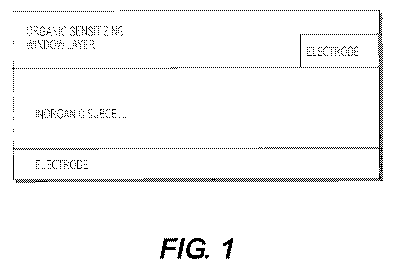
[0040] Figure 1 is a schematic of a non-limiting example of a
photosensitive optoelectronic device in accordance with the present
disclosure.
[0041] Figure 2 is a schematic of a non-limiting example of a
photosensitive optoelectronic device comprising a p-n junction in accordance
with
the present disclosure.
[0042] Figure 3 is a schematic depicting the Dexter energy transfer from
the singlet fission material of the organic sensitizing window layer to the
inorganic
subcell.
[0043] Figure 4 shows recombination, generation and transfer dynamics of
the direct Dexter transfer of triplets to the inorganic subcell following
singlet fission.
CBM = conduction band minimum, and VBM = valence band maximum.
[0044] Figure 5 is a schematic of an exemplary energy matching GaAs
solar cell structure. The arrows indicate incident solar radiation. The open
circle is
the tetracene excited state. The tetracene single crystal is attached by
pressure
welding to the energy matching surface of the GaAs solar cell grown by
molecular
beam epitaxy.
[0045] Figures 6A and 6B are schematics depicting the singlet fission
process whereupon absorption of a high energy photon by the singlet fission
host,
the host undergoes fission into two triplets, which are transferred to the
phosphorescent emitter dopant.
[0046] Figure 7 charts theoretical calculations of (a) power conversion
efficiency (PCE) of an inorganic solar cell with bandgap EG utilizing an
organic
sensitizing window layer in accordance with the present invention, and (b)
optimized
11
CA 02886454 2015-03-26
WO 2014/052530
PCT/US2013/061828
inorganic solar cell EG for a given fission sensitizer ES-SF, and
corresponding PCE
limit.
[0047] Figure 8 charts theoretical calculations of maximum PCE when
considering the endothermic processes in fission sensitized phosphorescence.
[0048] Figure 9 depicts the outcoupling process from a singlet fission
coating.
[0049] Figure 10 shows absorption and emission spectra of DPT and
PtTPBP, as well as transitions and their rates in the DPT/PtTPBP system
determined
by ultrafast spectroscopy.
[0050] Figure 11 shows examples of platinum based porphyrin emitters.
[0051] Figure 12 shows the absorbance of vacuum deposited
diphenylisobenzofuran (DPIBF) with and without a PTCDA template layer.
[0052] Figure 13 illustrates linked dimers leading to prompt singlet
fission.
[0053] As used herein, the term "singlet fission material" or "singlet
fission
host" means a material that exhibits an excitation singlet energy (Es_sF) and
an
excitation triplet energy (E-1-5F) satisfying the following condition: ES-SF
2ET_sF. For
purposes of satisfying the condition under the present disclosure, an Es_sF
within 0.2
eV of 2E-r_sF is considered "equal to" 2ET-sF, and thus satisfies the
condition.
[0054] As used herein, the term "layer" refers to a member or component
of a photosensitive device whose primary dimension is X-Y, i.e., along its
length and
width. It should be understood that the term layer is not necessarily limited
to single
layers or sheets of materials. In addition, it should be understood that the
surfaces
of certain layers, including the interface(s) of such layers with other
material(s) or
layers(s), may be imperfect, wherein the surfaces represent an
interpenetrating,
12
CA 02886454 2015-03-26
WO 2014/052530
PCT/US2013/061828
entangled or convoluted network with other material(s) or layer(s). Similarly,
it
should also be understood that a layer may be discontinuous, such that the
continuity of the layer along the X-Y dimension may be disturbed or otherwise
interrupted by other layer(s) or material(s).
[0055] The terms "electrode" and "contact" are used herein to refer to a
layer that provides a medium for delivering photo-generated current to an
external
circuit or providing a bias current or voltage to the device. That is, an
electrode, or
contact, provides the interface between the active regions of a photosensitive
optoelectronic device and a wire, lead, trace or other means for transporting
the
charge carriers to or from the external circuit. Anodes and cathodes are
examples.
[0056] As used herein, the term "III-V material" may be used to refer to
compound crystals containing elements from group IIIA and group VA of the
periodic
table. More specifically, the term III-V material may be used herein to refer
to
compounds which are combinations of the group of Gallium (Ga), Indium (In) and
Aluminum (Al), and the group of Arsenic (As), Phosphorous (P), Nitrogen (N),
and
Antimony (Sb). Representative materials may include GaAs, InP, InGaAs, AlAs,
AlGaAs, InGaAsP, InGaAsPN, GaN, InGaN, InGaP, GaSb, GaAlSb, InGaTeP, and
InSb and all related compounds.
[0057] As described herein, the inorganic subcell is "positioned
between"
or "deposited between" the two electrodes if it is physically positioned in a
manner
such that the inorganic subcell is electrically between the two electrodes in
that holes
flow from the inorganic subcell to one electrode and electrons flow from the
inorganic
subcell to the opposing electrode.
[0058] The present disclosure relates to a photosensitive optoelectronic
device comprising two electrodes, an inorganic subcell positioned between the
two
13
CA 02886454 2015-03-26
WO 2014/052530
PCT/US2013/061828
electrodes, wherein the inorganic subcell comprises at least one inorganic
semiconductor material having a band gap energy (EG), and an organic
sensitizing
window layer disposed on the inorganic subcell. A non-limiting example of this
device is shown in Fig. 1. The organic sensitizing window layer may be in
physical
contact with the at least one organic semiconductor material having a band gap
energy (EG). In some embodiments, the organic sensitizing window layer is not
in
physical contact with the at least one organic semiconductor material having a
band
gap energy (EG).
[0059] The inorganic subcell referred to and depicted herein may
comprise
a p-n junction, e.g., any p-n junction known in the art for a conventional,
high-
efficiency inorganic solar cell. This is shown in Figure 2. While Figure 2
shows a
simple inorganic subcell comprising a base and an emitter forming a p-n
junction, it
should be appreciated that the inorganic subcell may comprise additional
layers as
known in the art for an inorganic solar cell and/or that the p-n junction may
be
oriented in any manner known in the art. The p-n junction may comprise at
least one
semiconducting material chosen from, for example, III-V materials Ge, Si,
CdTe,
ZnTe, copper indium gallium (di)delenide (CIGS), and combinations thereof. In
some embodiments, the III-V materials are GaAs, InP, GaN, and AIN.
[0060] The organic sensitizing window layer as described herein is
designed to increase the efficiency of the underlying inorganic subcell.
[0061] In one aspect, the organic sensitizing window layer comprises a
singlet fission material. The singlet fission material may exhibit an
absorptivity of
light of at least 103 cm-1 at one or more wavelengths ranging from 300 to 700
nm.
[0062] In this aspect, upon absorption of light by the singlet fission
material, energy transfer to the underlying inorganic subcell occurs by direct
Dexter
14
CA 02886454 2015-03-26
WO 2014/052530
PCT/US2013/061828
(i.e. non-radiative) transfer of energy from the triplet state of the singlet
fission
material upon diffusion to the interface of the organic layer and the
inorganic subcell.
Thus, in some embodiments, the singlet fission material exhibits an excitation
triplet
energy (E-r_sF) substantially matching the band gap energy EG of the at least
one
inorganic semiconductor material. "Substantially matching" as used throughout
this
disclosure means an energy difference 0.3 eV. In some embodiments, the energy
difference is 0.2 eV, 0.1 eV, or 0.05 eV. The singlet/triplet energies of the
singlet fission material may be fine-tuned by donor/acceptor and/or nitrogen
substitution. In this way, the excitation triplet energy (E-r_sF) of the
singlet fission
material may be tuned to substantially match the band gap energy EG of the at
least
one inorganic semiconductor layer.
[0063] Another approach for substantially matching the excitation
triplet
energy (E-r_sF) of the singlet fission material with the band gap energy EG of
the at
least one inorganic semiconductor material is through the use of an inorganic
energy
matching layer. Thus, in some embodiments, the inorganic subcell comprises at
least one p-n junction and an inorganic energy matching layer positioned
between
the at least one p-n junction and the organic sensitizing window layer,
wherein the
inorganic energy matching layer comprises the at least one inorganic
semiconductor
material. In this embodiment, the band gap energy (EG) of the at least one
inorganic
semiconductor material can substantially match the excitation triplet energy
(E-r_sF) of
the singlet fission material. For example, the inorganic energy matching layer
can be
chosen to provide a band gap energy EG that substantially matches the
excitation
triplet energy (E-r_sF) of the singlet fission material. The at least one
inorganic
semiconductor layer may comprise a III-V material. As shown in the non-
limiting
example in Fig. 5, an InxGai_xAs energy matching layer is positioned between
the
CA 02886454 2015-03-26
WO 2014/052530
PCT/US2013/061828
organic sensitizing window layer and the emitter. By adjusting, for example,
the
ln/Ga concentration from x=0 to 0.2, the bandgap of this ternary can be tuned
from
1.42 eV to 1.1 eV. A singlet fission material, e.g., single crystal sheets of
tetracene,
can be grown by OVPD and directly attached to the InGaAs surface by a
technique
such as pressure welding. The growth can proceed on template substrates, by
nucleation on the cold walls of the OVPD reactor, or can be precipitated from
the
melt via solution growth.
[0064] The Dexter energy transfer referenced above is shown in Fig. 3.
The dashed oval shows the hybrid Wannier-Mott/Frenkel charge transfer state
formed by direct Dexter transfer from the singlet fission material to the
inorganic
subcell, such as a Si cell. As shown, following singlet fission, the triplet
exciton
diffuses to the interface of the organic layer and the inorganic subcell.
There, it
couples with the bands of the inorganic semiconductor, e.g., the at least one
semiconductor material having a band gap energy (EG), and transfers its energy
to
weakly bound inorganic exciton states, or directly to the band edge free
carrier
states. The inorganic excitonic states are rapidly thermalized, creating free
carriers.
One carrier type is collected at the back contact (emitter) of the cell, and
the counter
carrier is swept out to the top cell contact.
[0065] Fig. 4 also shows the direct energy transfer of a triplet state
of the
organic material into an inorganic semiconductor. The various rates (k) are
defined
as follow: kis is the rates of fission, kT is the rate of triplet decay, ks is
the rate of
singlet decay, koe, is the rate of Dexter transfer, and kre, is the rate of
free carrier
recombination in the inorganic semiconductor of the subcell. The "Dexter
energy
transfer" mechanism will dominate when the excitonic triplet state is non-
radiative.
The rate of Dexter transfer can be expressed as follows:
16
CA 02886454 2015-03-26
WO 2014/052530
PCT/US2013/061828
kDex= KJ,f exp(-2z/L) (1)
where K is a constant, J,f is the integral of the overlap between the emission
of
the triplet state and the absorption of the semiconductor medium (i.e. it is a
measure of the orbital energy resonance between the initial and final states
of the
excited species), z is the distance between the molecule and the
semiconductor,
and L is the characteristic tunneling distance. In sum, this process involves
the
coherent and simultaneous transfer of an electron and hole from the initial
(organic)
to the final (inorganic semiconductor) state over a distance z.
[0066] In accordance with equation (1), the free charge generation
within
the inorganic subcell should occur within a diffusion length, LD, of the
inorganic
subcell base region. Thus, the emitter layer, e.g., as shown in Fig. 3, should
be no
thicker than the electron diffusion length. It is also noted that native
oxides on the
inorganic subcell surface can present a barrier to triplet transfer. Thus, in
some
embodiments, a surface of the inorganic subcell is stripped by etching, e.g.,
with HF.
Additionally, CH3 terminated surfaces may give improved adhesion/wetting or
the
organic sensitizing window layer to the inorganic subcell surface, such as a
Si
surface.
[0067] In some embodiments, the thickness of the organic sensitizing
window layer is chosen so as not to exceed the triplet diffusion length of the
singlet
fission material. In certain embodiments, the thickness of the organic
sensitizing
window layer is in a range of 0.01 to 2 pm, 0.1 to 2 pm, or 0.1 to 1 pm. While
the
thickness of the organic sensitizing window layer should be chosen so as not
to
exceed the exciton diffusion length of the singlet fission material to prevent
triplet
loss to nonradiative decay, this is balanced by the desire to achieve high
optical
density in the window layer. Thus, in some embodiments, the singlet fission
material
17
CA 02886454 2015-03-26
WO 2014/052530
PCT/US2013/061828
exhibits long-range crystalline order. In some embodiments, the singlet
fission
material is a single crystal film. Such crystalline organic materials exhibit
long
diffusion lengths allowing for thicker organic sensitizing window layers
resulting in
higher optical densities. Organic materials of long range crystalline order
and
organic single crystal films may be grown using organic vapor phase deposition
(OVPD) techniques known in the art.
[0068] In some embodiments, the organic sensitizing window later
comprising the singlet fission material is in physical contact with the at
least one
inorganic semiconductor material of the inorganic subcell. In some
embodiments,
the organic sensitizing window layer comprising the singlet fission material
is within a
distance 2 nm from the at least one inorganic semiconductor material of the
inorganic subcell.
[0069] In some embodiments, the singlet fission material can be
deposited
on the surface of a templating layer, such as a 1 nm thick film of 3,4,9,10-
perylenetetracarboxylic dianhydride (PTCDA), to form a continuous film. For
example, deposition of diphenylisobenzofuran on the surface of PTCDA can
result in
a continuous film. Absorbance measurements of the deposited
diphenylisobenzofuran film confirms that the film has the same morphology as
required for 200% singlet fission efficiency, as shown in Fig. 12.
[0070] The singlet fission material may be chosen from materials that
satisfy the condition ES-SF 2ET-SF as defined above. Examples of suitable
singlet
fission materials include polyacenes, rylenes, rubrenes, and biradicaloids. In
certain
embodiments, the singlet fission material is chosen from anthracene, tetracene
(Es_
SF = 2.3 eV, ET_sF = 1.25 eV), pentacene, rubrene, and derivatives thereof. In
certain
embodiments, the singlet fission material is chosen from benzofurans and
related
18
CA 02886454 2015-03-26
WO 2014/052530
PCT/US2013/061828
compounds. Dimer molecules of these exemplary materials can also be
appropriate
for the singlet fission material. For example, a slipped stack arrangement can
be
formed by preparing acene dimers, such as tetracene dimers, around a
cyclophane
core as shown in Fig. 13A. Thus, a thick film of covalent dimers, either alone
or
doped into a host matrix may give prompt and efficient singlet fission.
Aromatic
linkages may also be employed, as shown in Fig. 13B. In some embodiments, the
acenes have close 7E-contact on an edge but not across a face. Molecules such
as
those depicted in Fig. 13C have an interacene spacing of close to 3 A on an
edge,
but since the 7E-systems are not coplanar, the balance of each acene is 4-5 A
distant
from the other. The R groups shown in Fig. 13 can be used to fine-tune the
acene
interaction by steric control.
[0071] In certain embodiments, the singlet fission materials may be
chosen
from materials that also satisfy the condition E(T-SF)2 > 2ET-SF, where E(T-
SF)2 is the
next highest triplet state.
[0072] The at least one inorganic semiconductor material as described
herein may comprise a material chosen from III-V materials, Si, Ge, CdTe,
ZnTe,
and copper indium gallium (di)selenide (CIGS). In certain embodiments, the at
least
one inorganic semiconductor material is chosen from GaAs, InP, GaN, AIN, and
InGaAs.
[0073] In another aspect, the organic sensitizing window layer comprises
a
singlet fission host and a phosphorescent emitter dopant, wherein the singlet
fission
host exhibits an excitation triplet energy (ET_sF) greater than or equal to an
excitation
triplet energy (ET_pE) exhibited by the phosphorescent emitter dopant. Under
the
present disclosure, an ET_sF within 0.2 eV of ET_pE is considered "equal to"
ET_pE. The
19
CA 02886454 2015-03-26
WO 2014/052530
PCT/US2013/061828
singlet fission host may exhibit an absorptivity of light of at least 103 cm-1
at one or
more wavelengths ranging from 300 to 700 nm.
[0074] In this aspect, a singlet produced upon the absorption of a high
energy photon by the singlet fission host undergoes fission into two triplets,
which
are transferred to the phosphorescent emitter dopant. This energy process is
shown
in Figs. 6A and 6B. As shown in the Figures, one absorbed high energy photon
produces two near infrared (NIR) photons emitted from the phosphorescent
emitter
dopant. The two NIR photons are subsequently absorbed in the inorganic
subcell,
producing two electrons, which increase the device's efficiency. The
improvement in
efficiency is limited only by the efficiency of singlet fission, the transfer
efficiency of
triplet energy from the singlet fission host to the phosphorescent emitter
dopant, the
phosphorescent efficiency of the emitter dopant, and the coupling efficiency
of the
emitted photons into the inorganic subcell.
[0075] To transfer the triplets of the singlet fission host to the
phosphorescent emitter dopant, the excitation triplet energy (ET_sF) of the
singlet
fission host should be greater than or equal to the excitation triplet energy
(ET_pE) of
the emitter dopant. In some embodiments, the excitation triplet energy of the
singlet
fission host substantially matches the excitation triplet energy of the
emitter dopant.
In addition, the rate of triplet transfer from the singlet fission host to the
phosphorescent emitter dopant should be faster than the rate of deactivation
of the
singlet or triplet excited states of the singlet fission host. The photons
emitted from
the phosphorescent emitter dopant should be of sufficiently high energy to be
absorbed in the active region of the underlying inorganic subcell. Thus, in
some
embodiments, the phosphorescent emitter emits radiation at an energy greater
than
CA 02886454 2015-03-26
WO 2014/052530
PCT/US2013/061828
or equal to the band gap energy (EG) of the at least one inorganic
semiconductor
material.
[0076] Fig. 10 shows the kinetics of energy transfer between 5, 12-
diphenyltetracene (DPT), a singlet fission host, and a phosphorescent
material:
platinum-tetraphenyl-tetrabenzo-porphyrin (PtTPBP). Although unmodified PtTPBP
has a higher triplet energy than the singlet fission host DPT, indicating that
this pair
of materials may not be a suitable combination of host and dopant, this
material
combination, as shown in the ultrafast spectroscopy data of Fig. 10, does
confirm
that the kinetics of energy transfer between singlet fission hosts and
phosphorescent
dopants are compatible, i.e., the phosphorescent dopant does not hinder prompt
singlet fission, and the rate of triplet exchange between the two materials is
rapid.
The short transfer times (35 ps) observed for triplet transfer between PtTPBP
and
DPT suggest that energy transfer to the phosphor is much more rapid than
direct
decay from either the singlet or triplet manifolds to the ground state. Also,
the rate of
triplet fusion in DPT is markedly lower than the fission rate, such that the
equilibrium
singlet (Si) to triplet state (Ti) reaction, Si + So <-> 2 Ti, is strongly
preferred.
[0077] The maximum power conversion efficiency (PCE) can be modeled
for a system based on singlet fission-sensitized phosphorescence coupled to an
inorganic subcell of bandgap EG. The upper limit to total system efficiency is
defined
by assuming that 100% of photons with energy > Es-sF are absorbed by the
singlet
fission host and subsequently emitted at ET-pE with 200% quantum efficiency.
Fig.
7A shows the calculated PCE of an inorganic solar cell with bandgap EG,
utilizing an
organic sensitizing window layer with singlet fission host singlet energy of
ES-SF, and
phosphorescent emitter dopant triplet energy of ET-pE = 1/2 Es-sF. As shown in
Fig.
7A, the abrupt increase when EG is decreased below ET-PE is due to the onset
of
21
CA 02886454 2015-03-26
WO 2014/052530
PCT/US2013/061828
absorption due to fission-sensitized phosphorescence. Fig. 7B shows the
calculated
optimized inorganic solar cell EG for a given Es-SF (left axis, assuming ET-pE
= 1/2 E5
SF), and the corresponding PCE limit (right axis). For a given EG, the PCE
peaks at
the optimized Es-sF (Fig. 7B, left axis). Thus, PCE reaches a maximum when EG-
1
eV (i.e. close to 1.1 eV for Si) and E5_5F-2 eV (Fig. 7B, right axis).
[0078] It has been shown that triplet transfer from the singlet fission
host to
the phosphorescent emitter dopant can be highly efficient even if the process
is
endothermic with an energy difference as large as 0.1 eV. Also, singlet
fission can
be endothermic by as much as 0.2 eV and still proceed with high efficiency.
Thus,
the overall process considers both endothermic processes such that the total
endothermic energy barrier is defined as A = ET-pE - 1/2 Es-sF. The result is
shown in
Fig. 8, where the maximum PCE is enhanced to 44.5%, 46.5%, and 47.5% when A =
0.1 eV, 0.2 eV and 0.3 eV, respectively. The energy difference is compensated
by
high energy photons prevalent in organic molecules. For example, the C-C
stretch
energy is ¨0.11 eV, and hence A = 0.3 eV is well within the energy range that
leads
to efficient endothermic transfer and fission.
[0079] The presence of endothermic transfer shifts the optimum band gap
of the underlying inorganic subcell to commensurately higher voltages. For
example,
at A = 0.3 eV, the maximum efficiency is achieved for EG = 1.3 eV. This is
only
slightly lower than that of GaAs (where EG = 1.42 eV). Thus, in some
embodiments,
the inorganic subcell comprises at least one p-n junction and an inorganic
energy
matching layer positioned between the at least one p-n junction and the
organic
sensitizing window layer, wherein the inorganic energy matching layer
comprises the
at least one inorganic semiconductor material. In this embodiment, the band
gap
energy (EG) of the inorganic energy matching layer can be tuned to optimize
the PCE
22
CA 02886454 2015-03-26
WO 2014/052530
PCT/US2013/061828
for a given single fission host/phosphorescent emitter dopant pair. The at
least one
inorganic semiconductor material may comprise a III-V material. As shown in
the
non-limiting example in Fig. 5, an InxGai_xAs energy matching layer is
positioned
between the organic sensitizing window layer and the emitter of the inorganic
subcell. The band gap of the matching layer can be tuned by varying x, i.e.,
varying
the ln/Ga concentration as discussed above.
[0080] One significant potential loss mechanism is the outcoupling
process
from the window layer. The loss is due to outcoupling from triplet remission
into 4-rr
solid angle from the phosphorescent emitter dopant as shown in Fig. 9. The
coupling efficiency is ultimately determined by the exit cone defined by the
critical
angle for total internal reflection at the organic/air interface. For most
organics
(index of refraction ¨2), a coupling efficiency into the inorganic subcell of
¨ 83% is
expected. The use of an antireflective coating on top of the organic
sensitizing
window layer may efficiently couple the UV-green region of the solar spectrum
into
the organic layer. The thickness of the organic layer may be tuned to enhance
coupling of the red-IR region of the solar spectrum directly into the
inorganic subcell.
Without employing such techniques to reduce outcoupling, based on these
estimates, the upper limit PCE is 0.83 x 47% = 39%.
[0081] In some embodiments, the organic sensitizing window layer
comprising the singlet fission host and the phosphorescent emitter dopant is
in
physical contact with the at least one inorganic semiconductor material of the
inorganic subcell. In some embodiments, the organic sensitizing window layer
comprising the singlet fission host and the phosphorescent emitter dopant is
within a
distance several microns, e.g., 5 microns, from the at least one inorganic
semiconductor material of the inorganic subcell. The organic sensitizing
window
23
CA 02886454 2015-03-26
WO 2014/052530
PCT/US2013/061828
layer comprising the singlet fission host and the phosphorescent emitter
dopant may
have a thickness in the range of 0.1 to 2 pm.
[0082] The singlet fission host may be chosen from materials that
satisfy
the condition ES-SF 2ET-SF as defined above. Examples of suitable singlet
fission
materials include polyacenes, rylenes, rubrenes, and biradicaloids. In some
embodiments, the polyacenes are anthracene, tetracene, pentacene, and
derivatives
thereof, and the biradicaloids are benzofurans and related compounds. Dimer
molecules of these exemplary materials can also be appropriate for the singlet
fission host. For example, a slipped stack arrangement can be formed by
preparing
acene dimers, such as tetracene dimers, around a cyclophane core as shown in
Fig.
13A. Thus, a thick film of covalent dimers, either alone or doped into a host
matrix
may give prompt and efficient singlet fission. Aromatic linkages may also be
employed, as shown in Fig. 13B. In some embodiments, the acenes have close 7E-
contact on an edge but not across a face. Molecules such as those depicted in
Fig.
13C have an interacene spacing of close to 3 A on an edge, but since the 7E-
systems
are not coplanar, the balance of each acene is 4-5 A distant from the other.
The R
groups shown in Fig. 13 can be used to fine-tune the acene interaction by
steric
control.
[0083] In certain embodiments, the singlet fission host comprises 5, 12-
diphenyltetracene (DPT) or derivatives thereof. In other embodiments, the
singlet
fission host comprises diphenylisobenzofuran or derivatives thereof. In some
embodiments, the singlet fission host exhibits an excitation singlet energy
Es_sF
greater than 2.0 eV. In certain embodiments, the singlet fission host may be
chosen
from materials that also satisfy the condition E(T-SF)2 > 2ET-SF, where E(T-
SF)2 is the
next highest triplet state of the singlet fission host.
24
CA 02886454 2015-03-26
WO 2014/052530
PCT/US2013/061828
[0084] The phosphorescent emitter dopant may be chosen to emit
radiation in the red/NIR spectral region. In some embodiments, the
phosphorescent
emitter dopant exhibits highest phosphorescence efficiencies in the red/NIR
spectral
region. The phosphorescent emitter dopant may comprise, for example, an
organometallic material. In some embodiments, the phosphorescent emitter
dopant
comprises a material chosen from metal porphyrins and phthalocyanines. The
metal
porphyrins may be chosen from, for example, platinum porphyrins. In certain
embodiments, the platinum porphyrins are platinum-tetraphenyl-tetrabenzo-
porphyrin
(PtTPBP), tetraphenyltetranaptho platinum porphyrin (PtTPNP),
tetraphenyltetraanthro platinum porphyrin (PtANP), platinum-
diphenyltetranaptho-
porphyrin (PtDPNP), and derivatives thereof. Fig. 11 shows the structure of
these
non-limiting examples of platinum porphyrins.
[0085] In some embodiments, the triplet excitation energy (ET_pE) of
candidate phosphorescent emitter dopants may be suitably tuned for use with a
singlet fission host. As described above, the excitation triplet energy
(ET_sF) of the
singlet fission host should be greater than or equal to the excitation triplet
energy (ET
PE)of the phosphorescent emitter dopant, so that the triplet localizes on the
phosphorescent emitter dopant and not the singlet fission host. For example,
extending conjugation at the benzopyrole rings as shown for the naptho-fused
materials in Fig. 11 shifts the triplet energy of the PtTPBP to wavelengths of
900 ¨
1000 nm. A similar emission energy is expected for acenaphthalene derivative,
PtANP, in Fig. 11.
[0086] In some embodiments, deuterium is substituted for hydrogen in the
phosphorescent emitter dopant to increase phosphorescence yields. In certain
CA 02886454 2015-03-26
WO 2014/052530
PCT/US2013/061828
embodiments, deuterium is substituted for hydrogen in the metal porphyrin
based
dopants.
[0087] In a specific embodiment, the singlet fission host is
diphenylisobenzofuran (Es-SF = 2.76 eV, ET-SF = 1.4 eV) and the phosphorescent
emitter dopant is PtTPNP (ET_pE = 1.38 eV).
[0088] In some embodiments, the blend of singlet fission host and
phosphorescent emitter dopant can be deposited on the surface of a templating
layer, such as a 1 nm thick film of 3,4,9,10-perylenetetracarboxylic
dianhydride
(PTCDA), to form a continuous film. The deposition, for example, of
diphenylisobenzofuran on the surface of PTCDA is described above and results
are
shown in Fig. 12.
[0089] In some embodiments, the ratio of singlet fission host to
phosphorescent emitter dopant in the organic sensitizing window layer may
range
from 10:1 to 1:1.
[0090] The two electrodes referenced herein may comprise an anode and
a cathode. Electrode materials known in the art may be used. Examples include
Al,
Ag, Au, Cu, or other common metals and inorganic compounds such as oxides,
e.g.
indium tin oxide (ITO), fluorine doped tin oxide (FTO) gallium doped zinc
oxide, or
metal halides, e.g. Cul.
[0091] In another aspect of the present disclosure, there is disclosed a
method of fabricating a photosensitive optoelectronic device comprising
depositing
an inorganic subcell between two electrodes, wherein the inorganic subcell
comprises at least one inorganic semiconductor material having a bandgap (EG),
and
depositing an organic sensitizing window layer on the inorganic subcell,
wherein the
organic sensitizing window layer comprises a singlet fission material.
26
CA 02886454 2015-03-26
WO 2014/052530
PCT/US2013/061828
[0092] The inorganic subcell may be deposited according to techniques
known in the art for fabricating inorganic solar cells. In some embodiments,
the
inorganic subcell is deposited by gas-source molecular beam epitaxy.
[0093] The organic sensitizing window layer may be deposited on the
inorganic subcell by vapor phase methods, for example, vacuum thermal
evaporation or organic vapor phase deposition. The organic sensitizing window
layer may also be deposited by solution based methods, such as spin coating,
spray
coating, gravure printing, ink-jet printing, and other solution based methods.
[0094] In some embodiments, the inorganic subcell comprises at least one
p-n junction and an inorganic energy matching layer positioned between the at
least
one p-n junction and the organic sensitizing window layer, wherein the
inorganic
energy matching layer comprises the at least one inorganic semiconductor
material,
wherein the band gap energy (EG) substantially matches an excitation triplet
energy
(E-r_sF) of the singlet fission material. In certain embodiments, the at least
one
inorganic semiconductor material comprises a III-V material. In certain
embodiments, the III-V material is InxGai_xAs, wherein x is chosen to tune the
band
gap energy EG to substantially match the excitation triplet energy (E-r_sF) of
the
singlet fission material.
[0095] In another aspect of the present disclosure, there is disclosed a
method of fabricating a photosensitive optoelectronic device comprising
depositing
an inorganic subcell between two electrodes, wherein the inorganic subcell
comprises at least one inorganic semiconductor material having a bandgap (EG),
and
depositing an organic sensitizing window layer on the inorganic subcell,
wherein the
organic sensitizing window layer comprises a singlet fission host and a
phosphorescent emitter dopant, the singlet fission host exhibiting an
excitation triplet
27
CA 02886454 2015-03-26
WO 2014/052530
PCT/US2013/061828
energy (ET_sF) greater than or equal to an excitation triplet energy (ET_pE)
exhibited by
the phosphorescent emitter dopant.
[0096] Unless otherwise indicated, all numbers expressing quantities of
ingredients, reaction conditions, and other properties or parameters used in
the
specification are to be understood as being modified in all instances by the
term
"about." Accordingly, unless otherwise indicated, it should be understood that
the
numerical parameters set forth in the following specification and attached
claims are
approximations. At the very least, and not as an attempt to limit the
application of
the doctrine of equivalents to the scope of the claims, numerical parameters
should
be read in light of the number of reported significant digits and the
application of
ordinary rounding techniques.
[0097] Other embodiments of the invention will be apparent to those
skilled
in the art from consideration of the specification and practice of the
invention
disclosed herein. It is intended that the specification be considered as
exemplary
only, with a true scope and spirit of the invention being indicated by the
following
claims.
28