Note : Les descriptions sont présentées dans la langue officielle dans laquelle elles ont été soumises.
CA 02888597 2015-04-16
WO 2014/060648 PCT/F12013/050987
BENT OPTICAL WAVEGUIDE
FIELD OF THE INVENTION
Generally the present invention relates to optics and photonics. In
particular,
however not exclusively, the present invention concerns HIC (high index con-
trast) optical multi-mode waveguides and bending thereof.
BACKGROUND
Optical waveguides including multi-mode dielectric waveguides are designed for
the transmission of electromagnetic waves in the optical band. An optical wave-
guide is basically a light conduit configured, by means of properly selected
core
and surrounding cladding materials with higher and lower refractive indexes,
re-
spectively, to confine and transport light therein without leaking it to the
envi-
ronment.
Optical waveguides can be classified according to their geometry (slab
(planar)
or strip, cylindrical, etc.), mode structure (single-mode, multi-mode),
refractive
index distribution (step or gradient index) and e.g. material (glass, polymer,
sem-
iconductor, etc.). Refraction of light at the core/cladding interface is
generally
governed by the Snell's law. When light arrives at the interface between the
core
and cladding materials above a so-called critical angle it is completely
reflected
back into the core material based on a phenomenon called 'total internal
reflec-
tion' (TIR).
In terms of wave-optics, a multi-mode waveguide is, as the name alludes,
capable
of guiding the waves of several modes, i.e. a discrete set of solutions of Max-
well's equations with boundary conditions, in addition to the main mode. In
prac-
tice, the larger the core dimensions of the waveguide the greater the number
of
modes is. The multi-mode waveguides and related equipment for interfacing the
light with the waveguide are typically easier to construct than the single-
mode
counterparts due to e.g. larger dimensions generally enabling the utilization
of
coarser, more affordable hardware and manufacturing methods. However, mul-
timode distortion limits the 'bandwidth x distance' product of multi-mode wave-
guides in contrast to single-mode solutions. It also complicates (or prevents)
the
realization of advanced waveguide circuits that densely integrate a large
number
CA 02888597 2015-04-16
WO 2014/060648 PCT/F12013/050987
2
of waveguide components (couplers, filters etc.). Therefore, such circuits are
typ-
ically realized with single-mode waveguides, while multimode waveguides are
mainly used in point-to-point links and to realize relatively simple waveguide
circuits.
Multimode waveguides can also be locally used as part of single-mode wave-
guide circuits. They can form components, such as multi-mode interference
(MMI) couplers, where multiple modes are temporarily excited, but the light
eventually couples back into single-mode waveguides. They can also be used to
propagate light only in the fundamental mode, but in this case light must be
cou-
pled adiabatically between the single and multimode waveguide sections to
avoid
the excitation of higher order modes. And finally, multimode waveguides can be
placed behind single-mode waveguides when multimode distortion is no longer
relevant, for example when coupling light into a large-area photodetector.
By definition, the modes of a multi-mode straight waveguide propagate unper-
turbed without mutual coupling, unless some perturbation occurs, such as a
change in the waveguide shape. In particular, bends can induce significant cou-
pling between the different modes such that in the straight section at the end
of
the bend, also higher order modes (HOM) will be in general excited, even if
only
the fundamental mode was excited in a straight section preceding the bend. The
higher the curvature 1/R (bend radius R), the higher is the degree of unwanted
coupling and, in general, also the higher the number of significantly excited
modes.
Indeed, one basic design rule of single-moded photonic integrated circuits dic-
tates that any bent waveguide must be single-moded so that the undesired cou-
pling between the modes and subsequent detrimental mode beating and power
radiation in the bend may be avoided. For integration purposes the bend radius
is
typically to be minimized, which requires the use of HIC waveguides. Further,
the higher the index contrast the smaller the waveguide shall be in order to
ensure
the single-mode condition. Sub-micron waveguides could be utilized for achiev-
ing dense integration, but they pose many additional challenges, including
polar-
ization dependence and low coupling efficiency to optical fibre modes. Further-
more, for scalable production they require expensive state-of-the-art
fabrication
tools in order to resolve submicron features and are also very sensitive to na-
nometer-scale fabrication errors.
CA 02888597 2015-04-16
WO 2014/060648 PCT/F12013/050987
3
As a reference one may introduce a single-moded rib waveguide that can be real-
ized on a silicon-on-insulator (SOT) wafer by dry etching the originally 4 jam
thick Si layer down to approximately 2 um thickness around an unetched 3.5 pm
wide rib that forms the waveguide. Despite its large dimensions and high index
contrast this waveguide is single-moded because the higher order modes radiate
power away from the rib along the surrounding 2 um thick Si slab. However, the
slab also enables the fundamental mode to radiate power into the slab when the
rib waveguide is bent. Therefore the minimum bending radius for such a rib
waveguides is approximately 4 mm. To avoid the radiation losses of the funda-
mental mode in a bend the rib waveguide can be locally converted into a multi-
mode strip waveguide or the etch depth can be locally increased around the
bend
[Reference: K. Solehmainen, T. Aalto, J. Dekker, M Kapulainen, M. Harjanne
and P. Heimala, "Development of multi-step processing in silicon-on-insulator
for optical waveguide applications", Journal of Optics A: Pure and Applied 0p-
tics, vol 8, pp. S455-S460 (2006)]. However, in practice this has led to the
inevi-
table excitation of HOMs if the bending radius has been reduced by a factor of
10
or more with respect to the corresponding low-loss rib waveguide bend.
The goal of shrinking the bend radius of multimode HIC waveguides could be
sought by a matched arc approach, which relies on matching the length of a cir-
cular bend to an integer multiple of beating lengths between the fundamental
mode and the first higher order mode (HOM) of the bent waveguide to ensure
that, at the end of the bend, only the fundamental mode will be excited
despite
the fact that HOMs have been excited during propagation in the bent section.
Nevertheless, the obtained bending radii are still relatively large, in
practice e.g.
two orders of magnitude larger than the waveguide width, and in particular,
manufacturing thereof is challenging due to very stringent tolerance require-
ments.
SUMMARY OF THE INVENTION
The objective is to at least alleviate one or more aforesaid problems and to
pro-
vide an optical multi-mode HIC waveguide with improved, tight bend(s).
The objective is achieved by different embodiments of an optical multi-mode
HIC waveguide for transporting electromagnetic radiation in the optical wave-
band, the waveguide comprising guiding core portion with higher refractive in-
dex, and cladding portion with substantially lower refractive index configured
to
CA 02888597 2015-04-16
WO 2014/060648 PCT/F12013/050987
4
at least partially surround the light guiding core in the transverse direction
to fa-
cilitate confining the propagating radiation within the core, the waveguide
being
configured to support multiple optical modes of the propagating radiation,
wherein the relative refractive index contrast between said core and cladding
por-
tions is about 25% or higher, and the waveguide incorporates a bent waveguide
section having a bend curvature that is configured to at least gradually,
preferably
substantially continuously, increase towards a maximum curvature of said sec-
tion from a section end.
The maximum curvature of the bent section may appear at either end of the sec-
tion or between the ends thereof such as half-way the section length. In the
latter
case, either or both of the ends may be associated with the common minimum
curvature of the section, or contain at least local minima. The curvature may
in-
.. crease towards the maximum from one end and decrease away therefrom to the
other end of the section. Both section ends may be substantially straight
while the
bent section is applied to change the direction of the waveguide. The section
ends
may be mutually parallel or non-parallel. In some embodiments, the waveguide
may consist of the bent section. Alternatively, the waveguide may also define
a
plurality of further sections each of which is straight or bent. Generally,
several
bent sections may also be joined together to construct more complex bend
shapes. For example, a substantially straight section could be followed by one
or
more bent sections and optionally a further substantially straight section. In
terms
of radiation propagation, one section end could be referred to as light input,
or
incoupling, end and the other as light output, or outcoupling, end.
Various optimized bend shapes such as 'U'-bends or `L'-bends, or a spiral seg-
ment shape, may be constructed utilizing the principle of the present
invention.
In one embodiment, the bent section contains two mirror-symmetric sub-sections
adjacent and substantially adjoining each other, the maximum curvature being
optionally realized at the border of said sub-sections, i.e. half-way the
overall
section length. For example, a "U' or `L' bend may be constructed accordingly.
As a further example of the application of symmetry in designing various bend
forms, a segment of a double-end spiral form could be constructed, wherein the
(center) point of symmetry bears the minimum curvature (straight).
CA 02888597 2015-04-16
WO 2014/060648 PCT/F12013/050987
In another, either supplementary or alternative, embodiment the curvature is
sub-
stantially linearly varying with the bend length so as to linearly increase
towards
the intermediate maximum from the minima at section ends.
5 In a further, either supplementary or alternative, embodiment the
effective bend
radius of curvature is in the order of magnitude of the waveguide width. As
the
curvature varies, the minimum radius is even smaller.
Yet in a ffirther, either supplementary or alternative, embodiment the core
portion
.. defines a substantially planar core layer and the cladding portion
optionally fur-
ther defines at least one substantially planar adjacent layer. Alternatively,
the
core portion defines a cylindrical inner core layer surrounded by the cladding
layer in transverse directions relative to the predetermined propagation
direction
(guiding direction) of the radiation.
Still, in a further, either supplementary or alternative, embodiment the
refractive
index (n) contrast between the core and cladding An = (ncore- ncla)/ncla is
sub-
stantially about 50% or higher, and preferably about 100% or higher.
In a further, either supplementary or alternative, embodiment the waveguide is
a
dielectric waveguide, preferably a strip waveguide. Preferably the core
comprises
dielectric material. Alternatively or additionally, the cladding may comprise
die-
lectric material.
In a further, either supplementary or alternative, embodiment the core portion
may be or include at least one material selected from the group consisting of:
semiconductor, Si, Ge, GaAs, InP, CdTe, ZnTe, silicon oxide, Si3N4, TiO2, pol-
ymer and diamond.
In a further, either supplementary or alternative, embodiment the cladding por-
tion may be or include at least one material selected from the group
consisting of:
air, silica containing glass, and polymer.
In a further, either supplementary or alternative, embodiment the bent section
de-
fines a matched bend (described hereinlater in more detail). Alternatively, it
may
define a generic, unmatched bend.
CA 02888597 2015-04-16
WO 2014/060648 PCT/F12013/050987
6
In various embodiments, the obtained waveguide may be of substantially micron
scale or smaller, for example.
An electronic, optical, optoelectronic and/or photonic device may comprise an
embodiment of the waveguide suggested herein. An optical circuit such as inte-
grated optical circuit may comprise an embodiment of the waveguide suggested
herein. A microring element such as a microring resonator may comprise an em-
bodiment of the waveguide suggested herein. Optionally multi-stage cascaded
MZI (Mach-Zehnder interferometer) may comprise an embodiment of the wave-
guide suggested herein. Optionally long and low-loss delay line may comprise
an
embodiment of the waveguide suggested herein. Also an MMI reflector (MMI
coupler with the two outputs connected with a U-bend) may comprise an embod-
iment of the waveguide suggested herein. Different communications or sensor
devices incorporating an embodiment of the presented waveguide may be manu-
factured.
The utility of the suggested solution arises from multiple issues depending on
the
embodiment. For example, ultra-small bends with low losses in micron-scale
HIC multimode waveguides may be obtained. Both matched and generic (un-
matched) bends with varying curvature may be capitalized. The applicable
bandwidth may be considerably large. The designed bends feature minimal bend-
ing radii comparable to the waveguide width. Experimental results further con-
firm the overall effectiveness, robustness and low losses of the realized
bends. As
an outcome, the 'footprint', i.e. the occupied surface area, and cost of the
associ-
ated circuits are reduced and previously unaffordable elements may become fea-
sible.
For example, the size of multi-mode interferometric reflectors may be remarka-
bly shrunk. On the other hand, bends with larger radii and lower losses may be
used, for example, to design long spirals with low footprint. E.g. an area of
about
0.5x0.5 inm2 could somewhat easily allocate an 8 cm long spiral. The proposed
bends are also expected to enable the fabrication of microring resonators with
high finesse. Various embodiments of the present invention are suitable for
use
with SOI (silicon-on-insulator) platforms including thicker SOIs and
interfacea-
ble with optical fibres. Micron-scale features of the proposed designs allow
for
fabrication with relaxed lithographic resolution by tools that are much less
ex-
pensive than the ones usually needed for scalable production of nanophotonic
devices. High confinement of light in multi-mode HIC waveguides makes the
7
proposed solution much less sensitive to fabrication errors, wavelength
changes and mode
polarization than the existing nanophotonic counterparts.
Generally, waveguides with small birefringence, good fiber coupling, and
robustness to
fabrication errors, may be obtained in contrast to e.g. fixed curvature bends
and/or nanophotonic
waveguides.
The expression "a number of" refers herein to any positive integer starting
from one (1), e.g. to
one, two, or three.
The expression "a plurality of' refers herein to any positive integer starting
from two (2), e.g. to
two, three, or four.
The expression "effective bend radius" (Reff) refers herein to the radius of
an arc that has the
same starting and final points and the same starting and final directions with
the bend of the
present invention.
The term "HIC" refers herein to high index contrast at least in the direction
of the bend radius,
and at least on the outer side of the bend regarding e.g. a rib waveguide with
a lateral groove,
whereas the contrast may be either high or low in the perpendicular direction,
i.e. the direction of
the bending axis.
The term "optical waveband" refers herein to frequencies between about 250 nm
and 10000 nm
thus including visible light and part of ultraviolet and infrared bands. The
provided waveguide
may be configured to operate in a number of selected sub-ranges only.
The terms "a" and "an", as used herein, are defined as one or more than one.
According to one aspect of the invention, there is provided an optical multi-
mode high index
contrast (HIC) waveguide, for transporting electromagnetic radiation in an
optical waveband, the
waveguide comprising:
CA 2888597 2019-11-27
7a
a guiding core portion made of a material having a first refractive index,
a cladding portion made of a material having a refractive index lower than the
first
refractive index, the cladding portion configured to at least partially
surround the guiding core
portion in a transverse direction to facilitate confining the propagating
electromagnetic radiation
within the guiding core,
a bent waveguide section defined by section ends comprising bent portions of
the guiding
core portion and the cladding portion, the bent waveguide section including a
bend curvature that
is configured to gradually increase towards a maximum curvature value from one
of the section
ends within said waveguide section in the direction of another section end,
the waveguide being configured to support multiple optical modes of the
transported
electromagnetic radiation, and,
wherein a relative refractive index contrast between said guiding core and
said cladding,
portion is about 25% or higher.
Various different embodiments of the present invention are also disclosed in
the dependent
claims.
BRIEF DESCRIPTION OF THE RELATED DRAWINGS
.. Next the invention is described in more detail with reference to the
appended drawings in which
CA 2888597 2019-11-27
CA 02888597 2015-04-16
WO 2014/060648 PCT/F12013/050987
8
Fig. 1 illustrates the basic principles of the present invention via different
appli-
cable bend shapes.
Fig. 2 illustrates an `L'-bend (90 deg bend) in accordance with an embodiment
of
the present invention.
Fig. 3a illustrates a `U'-bend (180 deg bend) in accordance with an embodiment
of the present invention.
Fig. 3b illustrates an 'S' bend in accordance with an embodiment of the
present
invention.
Fig. 4 depicts bend curvature change according to an embodiment of the present
invention.
Fig. 5a illustrates power coupling in the case of a prior art 90 deg arc bend
as a
function of bend radius.
Fig. 5b illustrates power coupling in the case of a `L'-bend (90 deg bend) in
ac-
cordance with an embodiment of the present invention as a function of the
effec-
tive bend radius.
Fig. 6a illustrates power coupling in the case of a typical matched 90 deg arc
bend from the standpoint of bandwidth utilization.
Fig. 6b illustrates power coupling in the case of a matched `L'-bend (90 deg
bend) according to an embodiment of the present invention from the standpoint
of bandwidth utilization.
Fig. 6c illustrates power coupling in the case of a generic (unmatched) `U-
bend
(90 deg bend) according to an embodiment of the present invention from the
standpoint of bandwidth utilization.
DETAILED DESCRIPTION OF THE EMBODIMENTS
In Figure 1 at 101, by way of example only, two different embodiments of the
present invention are generally illustrated at 102 and 104. Bends such as 'IP-
bends, `S'-bends, `L'-bends and practically any bend of a desired degree may
be
manufactured. Different basic bend shapes may be cleverly combined to
establish
more complex bends and (mirror/point) symmetry may be exploited to design the
bends.
For instance, two `U'-bends could be combined to form an `S'-bend, and the 'U'-
bend itself could be constructed from two mirror-symmetric halves, i.e. doubly
symmetric structures could be established. However, a skilled reader will
under-
stand such symmetry is not obligatory for utilizing the present invention to
estab-
CA 02888597 2015-04-16
WO 2014/060648 PCT/F12013/050987
9
lish bends, i.e. the bend portions preceding and following e.g. the point of
maxi-
mum curvature of a bend do not have to be mirror-symmetric.
The obtained bends are optically efficient and provide small footprint due to
op-
timized, yet small, non-constant bend radii. The order of magnitude of the
wave-
guide width and the bend radii may be substantially the same and e.g.
micrometer
scale configurations are achievable.
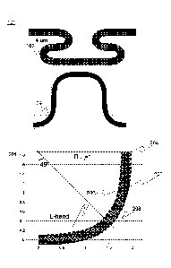
Fig. 2 illustrates, at 201, a cross-section (in the bend plane) of an `L'-bend
(90
deg bend) forming at least part, i.e. section, of an optical multi-mode HIC
wave-
guide in the direction of light propagation in accordance with an embodiment
of
the present invention and incorporating two mirror-symmetric bend sub-sections
202 with curvature linearly varying with length and bending radii normalized
to
the minimum value. The waveguide, such as a strip waveguide, further contains
core 204 and cladding 206 portions for transporting and confining light,
respec-
tively. It shall be noted that in some embodiments the cladding portion 206
may
be formed by non-solid material, optionally gaseous material such as air. The
point of maximum curvature 208 is located half way the section length at the
border of the mirror-symmetric sub-sections 202.
Generally, instead of utilizing e.g. a generic prior art arc with constant
radius of
curvature for implementing the bend and thus abruptly changing between
straight
and curved (arc) portions, the radius of curvature is to be gradually,
preferably
substantially continuously, varied to produce the bend with more continuous
and
smoother transitions, while the bend size is minimized.
For the `L'-bend or practically any other bend of a given angle 0 joining two
straight waveguides, two mirror-symmetric sections may be exploited, each of
them enabling bending by 0/2, which in the case of `L' implies using two
mirror-
symmetric 45 deg bends.
Figure 3a illustrates, at 301, a correspondingly designed, optimized `U'-bend
for
optical multi-mode HIC waveguide.
Reverting both to Fig. 2 and Fig. 3a, the linearly varying L-bend has an
effective
radius Reff = 1.87 Rmin, and in the case of the U-bend the effective radius is
Reff = 1.38 Rmin.
CA 02888597 2015-04-16
WO 2014/060648 PCT/F12013/050987
Figure 3b illustrates, at 302, one more embodiment of a bend, in this case an
bend, designed in accordance with the present invention.
5 With reference to Figure 4, the curvature (1/R) of a bend optimized
according the
teachings provided herein may change substantially linearly with the bend
length
as depicted. The curvature reaches a maximum value at half-length (radius R of
curvature is then at minimum) and reduces back to zero (or other minimum),
i.e.
mirror-symmetric bend realization is shown.
As a mathematical background regarding various embodiments of the present in-
vention, a bend with curvature that is linearly varying with path length may
be
characterized by means of so-called Euler spiral, which can be accurately
calcu-
lated through expansion series of Fresnel integrals (for practical purposes 2
or 3
expansion terms are usually sufficient). Therefore, the associated bends are
also
called hereinafter as 'Euler bends'.
For example, the effective or minimum radius of the applied bend curvature may
substantially be in the order of magnitude of the waveguide width, preferably
about 20 times the waveguide width or smaller, more preferably about ten times
the width or smaller, and most preferably about two times the width or
smaller.
Figures 5a and 5b illustrate modeled power coupling to different modes at the
output (straight) of 2 jam wide silicon strip waveguide with generic 90 degree
arc and Euler 'I.,' bends, respectively, as a function of the constant bend
radius
(arc) or the effective bend radius (Euler bend, in which case the minimum
radius
is 1.87 times smaller). The wavelength is 1.55 lam.
As a person skilled in the art will immediately realize from the coupling
curves
501 of Fig. 5a relating to a prior art arc, up to 4 HOMs can be excited by
about
1% (-20 dB) or more.
At Rz 1 I jam there seems to be a first resonant coupling to the fundamental
(0th
order) mode, but with poor suppression of coupling to 1st, 2nd and 3rd HOMs,
resulting in just about 90% output into the fundamental mode. The first
practical-
ly useful resonance (i.e. the lowest order low-loss matched bend) corresponds
to
Rz34.4 !Am, with fundamental mode coupling > 99%. For larger R values there
are other matched bend occurrences and all HOMs, except 1st order, can be ne-
CA 02888597 2015-04-16
WO 2014/060648 PCT/F12013/050987
11
glected in practice. The power oscillations between this mode and the fundamen-
tal mode slowly damp with R and for R>400 gm the maximum coupling to the
HOM is suppressed by more than 20 dB. One could adopt e.g. such suppression
level as the threshold to define the minimum R value ensuring low-loss
operation
of the bend. Unlike with the matched bend case, where power is significantly
coupled to HOMs in the bent section and then completely coupled back to the
fundamental mode at the very end of the bend, proper unmatched operation re-
quires that coupling to HOMs is always suitably suppressed during propagation.
In other words, the matched-bend is a resonant system, whereas the generic un-
matched bend is not. It is clear that unmatched operation ensures broader
opera-
tion bandwidth and higher tolerance to fabrication errors. In general, in any
bend
of any shape (i.e. with non-constant curvature) one can distinguish between
two
working principles: a resonant one based on matching the bend length to the
beating length between fundamental and HOMs - so ensuring high coupling into
the fundamental mode at the very end of the bend only - and another one simply
ensuring low coupling to HOMs at any propagation step.
Reverting to the coupling curves 503 of Fig. 5b, the modeled generic, i.e. un-
matched with reference to the above discussion, bend corresponds to Reff = 75
gm, i.e. more than 5 times smaller than the generic arc. Furthermore, the
first
useful matched bend occurs at Reff = 16.6 gm, i.e. at less than half the size
of the
smallest matched arc, and the second one at Reff = 37.4 gm, which is compara-
ble with the arc bend, but with much better performance.
Figures 6a, 6b, and 6c illustrate power coupling in the case of a prior art
type 90
deg arc bend, matched l'-bend according to an embodiment of the present in-
vention, and generic l'-bend according to another embodiment of the present
invention, respectively, from the standpoint of bandwidth utilization. As a
moti-
vation for such contemplation, it is typically beneficial to analyze the
spectral re-
sponse of the bends for various reasons. The responses reflect the associated
bends' tolerance to fabrication errors since one important design parameter is
the
ratio between the waveguide size and the wavelength, whereupon changing the
wavelength is like changing the size and vice-versa. It shall be noted that in
the
depicted case the matched bends were not precisely set to the transmission
peak
.. for 1.55 gm wavelength, but were optimized slightly off-resonance to ensure
the
highest operation bandwidth.
CA 02888597 2015-04-16
WO 2014/060648 PCT/F12013/050987
12
Besides the size shrinkage, the comparison between the smallest matched arc
(Fig. 6a) and the smallest matched Euler L-bend (Fig. 6b) highlights an order
of
magnitude broader bandwidth (indicated by the shaded rectangular areas) for
the
Euler L-bend. Also the generic Euler L-bend (Fig. 6c) yields excellent perfor-
mance. These simple examples show that the matched and generic Euler bends
can be not only much smaller than corresponding matched and generic arc bends,
but also perform great in terms of bandwidth and tolerances to fabrication
errors.
Similar results hold for different waveguide widths and different bend angles.
From the previous spectral analysis one may further derive a general
guideline: in
order to design a bend working in a given wavelength range, the bend should be
targeted to the smaller wavelengths of that range, and then optimized to cover
the
broadest possible range of longer wavelengths.
Furthermore, a design that works at a given wavelength X1 can be always re-
sealed to a different wavelength X2 by simply resealing waveguide width and
bending radii by a factor X2/X1 advantageously supplemented with some minor
optimization to take into account effective refractive index dispersion of the
giv-
en waveguide.
Even with a highly multi-mode ,-=1 t.tm wide waveguide, it is possible, for
exam-
ple, to design low loss (<0.1 dB per 180 ) matched Euler `1P-bends with Reff
1.4 !Lim like the ones shown in Fig. 1 at 102 or e.g. a generic Euler bend
with
Reff l tm in the case of 500 nm wide waveguide. This is superior to the con-
temporary solutions in connection with standard nanophotonic circuits based on
single mode waveguides, where the minimum bending radius is limited to about
2 um, because both submicron waveguide thickness and width, required for sin-
gle-mode operation, significantly lower the index contrast, also making the
mode
much more affected by sidewall-roughness-induced loss.
Still, the experimental results show that sonic of the designed bends have
losses
<0.05 dB. Thus a plurality of bends may be cascaded without inducing unac-
ceptable losses to the aggregate solution.
A skilled person may on the basis of this disclosure and general knowledge
apply
the provided teachings in order to implement the scope of the present
invention
as defmed by the appended claims in each particular use case with necessary
modifications, deletions, and additions, if any.
CA 02888597 2015-04-16
WO 2014/060648 PCT/F12013/050987
13
In the context of the present invention, the (radius of) bend curvature is
indeed
preferably gradually, most preferably substantially continuously, changed
instead
of constant curvature or abrupt changes, but in practical circumstances also
small
deviations from this basic rule may be implemented in the form of minor discon-
tinuation points, for example, to ease manufacturing or for some other reason
as
far as they don't induce too high losses.
Curvature dependence on path length doesn't have to be the linear symmetric
continuous function shown e.g. Fig. 4 (which defines the Euler spiral), but
may
be any other substantially continuous function starting from a smaller value
(preferably zero), reaching a maximum value and then typically going back to a
small value.
Further, the invention is generally applicable to e.g. any HIC dielectric
strip
waveguide, wherein the core may include any semiconductor like Si, Ge, GaAs,
InP, CdTe, ZnTe, and their compounds, or some other HIC material like doped or
undoped silicon oxide, Si3N4, TiO2, high-index polymer or diamond, while the
cladding can be established of any low index material such as air, silica
glasses,
polymers, etc. working at any wavelength.
As previously mentioned, the HIC condition is, in principle, mandatory in the
di-
rection of the bend radius only, and actually, the contrast may be high just
on the
outer side of the bend (e.g. a rib waveguide with a lateral groove). Index
contrast
is not a decisive factor in the perpendicular direction (i.e. the direction of
the
bending axis). The waveguide may be multi-mode in both directions.
Furthermore, the waveguide width may in general vary along the bend (e.g.
smaller width corresponding to smaller bending radii).
Considering the diversity of potential applications, the invention may have
useful
applications in connection with highly multi-mode waveguides (tens to hundreds
of microns in size) proposed e.g. for low cost optical interconnects on
printed
circuit boards. The invention can also be applied to nanophotonic silicon wave-
guides both to reduce bend losses and shrink bend sizes using multimode sec-
tions with large widths.
CA 02888597 2015-04-16
WO 2014/060648 PCT/F12013/050987
14
One interesting embodiment is strip waveguide technology with reference to
e.g.
micron scale Si cores (e.g. 1-10 um thickness and width) surrounded by silica,
that are intrinsically multi-mode in both directions. For instance, the light
may be
coupled from an optical fibre to the input (rib) waveguide of an integrated
circuit
or some other predetermined target element. Then when a small bend is needed,
the (rib) waveguide, which is preferably single-moded, may be converted into a
strip waveguide of suitable width that can be bent with very small footprint
and
high performances thanks to the present invention. Furthermore, conversion to
strip waveguides is anyway needed in many other devices as well (through
etched MMIs, AWGs, etc.), whereupon the invented tight and low-loss bends
will be also a useful alternative to the 90' turning mirrors that could be
used for
e.g. rib waveguides.
Still, the suggested bending approach is preferable whenever many cascaded
bends are needed, since the losses are clearly lower than with the turning
mirrors
(e.g. about 0.3 dB per turn).