Note : Les descriptions sont présentées dans la langue officielle dans laquelle elles ont été soumises.
CA 02890846 2015-05-07
- 1 -
ELECTRICALLY CONDUCTIVE SUPPORT FOR A GLAZING UNIT HAVING
LIQUID-CRYSTAL-MEDIATED VARIABLE SCATTERING PROPERTIES AND
SUCH A GLAZING UNIT
The invention relates to an electrode for a glazing unit
having liquid-crystal-mediated variable scattering properties,
equipped with a liquid-crystal layer that alternates
reversibly between a transparent state and a non-transparent
state, through application of an alternating electric field.
Glazing units are known certain properties of which can
be modified under the effect of a suitable supply of
electrical power, more particularly the transmittance,
absorptance and reflectance at certain wavelengths of
electromagnetic radiation, especially in the visible and/or in
the infrared, or even light scattering properties, can be
modified.
Electrically controllable
liquid-crystal-comprising
glazing units can be used anywhere, both in the architectural
field and in the automotive field, whenever sight through the
glazing unit must be prevented at given moments.
The electrodes conventionally used are made of mixed
indium tin oxide (ITO). In order to prevent short-circuits
being generated by conductive impurities that are greater than
or equal in size to the distance between the electrodes, each
of the ITO films may be coated with a film made of a
dielectric such as Si02 or Si3N4, as described in document US 5
808 715.
One object of the invention consists in providing a
multiple liquid-crystal-comprising glazing unit that is more
CA 02890846 2015-05-07
- 2 -
reliable and robust, without adversely affecting its optical
and electrical properties.
For this purpose, the present invention firstly provides
an electrically conductive support for a glazing unit having
liquid-crystal-mediated variable scattering properties,
comprising a first transparent substrate (made of mineral or
organic glass) having a main face comprising a multilayer of
thin films, in this order:
- (directly on the main face or on a thin underfilm, for
example made of metal oxide or nitride) an electrode
comprising a film, called the TCO film, based on a transparent
electrically conductive oxide (preferably based on tin and
indium) preferably having a thickness e0 lying in a range
extending from 50 to 200 nm;
- a silicon-nitride-based first barrier film (based on
SiN, and preferably Si3N4) that has a thickness el of at least 5
nm and that is undoped or optionally doped, preferably with
aluminium, and that preferably essentially consists of a
silicon nitride, optionally doped, preferably with aluminium;
and
- on (preferably directly on) the first barrier film, a
silicon-oxide-based second barrier film (based on SiOõ and
preferably Si02) that has a thickness e2 of at least 30 nm,
preferably of at least 45 nm or even 50 nm, and even more
preferably lower than or equal to 80 nm, and that preferably
essentially consists of silicon oxide (silica), this second
film being undoped or optionally doped, preferably with
aluminium;
the thickness el is smaller than e2, and/or el is smaller
than 80 nm;
CA 02890846 2015-05-07
- 3 -
the cumulative thickness eb of the first and second
barrier films is larger than or equal to 50 nm and smaller
than or equal to 150 nm, and even more preferably smaller than
or equal to 120 nm.
In the present invention the expression "barrier film" is
understood to mean a film providing a barrier to short-
circuits.
The Applicant has identified a number of sources of
short-circuits:
- conductive impurities of greater than or equal size to
the distance between the electrodes, as was already known, for
example metal particles (Al, stainless steel, etc.)
originating from splinters from machines for handling the
glass, contaminants of the glass (droplets of tin, etc.) or
even contaminants in the polymer/liquid crystal mixtures;
- but also conductive impurities of size smaller than the
distance between the electrodes, of the same origin,
particularly detrimental if irregularly shaped;
- non-conductive defects with a high dielectric constant
since the liquid crystals are then subjected to very high
electrical fields; and
- substantial roughness of the TCO film (producing
spikes, etc.).
The use of the at least two barrier films according to
the invention provides a more effective defence against these
multiple sources of short-circuits than all the monolayers of
the prior art because:
- the materials of the barrier films, and the minimum
values for el, e2 and eb are suitably selected; and
CA 02890846 2015-05-07
- 4 -
- the number of dielectric interfaces is increased,
thereby decreasing the number of defects (holes, grain
boundaries, pinholes, etc.) passing right through the films on
the TCO, which defects could allow short-circuits to form.
These two barrier films have a low dielectric
permittivity (typically lower than 10), a high breakdown
voltage (typically higher than 4 MV/cm), and a "self-healing"
breakdown mode.
For reasons relating to optical adjustment, the (Si0x)
second barrier film is chosen to have a lower refractive index
(in the visible) than the first barrier film.
The thicknesses eb and el are preferably also limited in
order to simplify the deposition conditions and ensure a good
mechanical strength is obtained. In contrast, giving the
second film a larger minimum thickness has the effect of
making the multilayer more effective as it significantly
reduces the frequency with which short-circuits are observed.
Advantageously, for optical reasons, the (Si0x) second
barrier film is preferably the last film, in particular the
last barrier film, or the last barrier film is separate from
the second barrier film and has a refractive index between 1.4
and 1.7 and even 1.4 and 1.55.
In the present application when a "succession of films"
or "successive films" is/are spoken of, or even when one film
is said to be located on or under another film, reference is
always being made to the process for manufacturing the
electrode, in which the films are deposited one after the
other on the transparent substrate. The first film is
therefore the film that is closest to the substrate, all the
CA 02890846 2015-05-07
- 5 -
"following" films being those located "on" the first film and
"under" the films deposited afterwards.
The term "film" will in the present invention, unless
otherwise specified, be used to refer to both a film made of a
single material (monolayer) and to several films each made of
a different material (multilayer).
In the present invention, unless otherwise indicated, the
term "thickness" is understood to mean geometric thickness.
In the present invention, the expression "based on" in
phrases of the form: a film based on oxide (based on nitride,
respectively) of a (or more than one) given metal element(s),
and the expression "-based" in phrases of the form: a metal-
oxide-based (metal-nitride-based, respectively) film, will be
understood to mean that the proportion by weight of the metal
element or elements is at least 50% of the total weight of
metal and preferably 70% of the total weight of metal.
According to the invention, unless otherwise specified,
if a film (oxide or nitride) is said to be doped, the term
"doped" will preferably be understood to mean that the metal
dopant is present in an amount smaller than 10% of the total
weight of metal in the film and even more preferably in an
amount smaller than 6% or even 5% of the total weight of metal
in the film.
In the present invention, in a film "essentially
consisting" of or that "essentially consists" of an oxide (or
a nitride) of a (or more than one) given metal element(s) and
of optional expressly defined metal dopants, the proportion by
weight of other metal elements (other than said elements and
dopants) is preferably smaller than 10% of the total weight of
metal and even more preferably smaller than or equal to 5%. In
CA 02890846 2015-05-07
- 6 -
other words, the proportion by weight of said metal elements
and metal dopants is preferably higher than 9096. of the total
weight of metal and even more preferably higher than or equal
to 9596 of the total weight of metal.
Furthermore, the term "metal" and the expressions "metal
element" and "metal dopant" include silicon and boron and in
addition all the metal elements of the periodic table (alkali
metals, alkali-earth metals, transition metals, post-
transition metals).
Naturally, according to the invention, a film
"essentially consisting" of or that "essentially consists" of
a given material may comprise other elements (impurities,
etc.) provided that they do not notably modify the desired
properties of the film.
According to the invention, if a film is said to be
"made" of a material, the term "made" is understood to be
synonymous with the expression "essentially consists".
According to the invention, the expression "thin film" is
understood to mean a film having a (geometric) thickness
smaller than 300 nm.
The films, especially the barrier films, are preferably
obtained by magnetron sputtering.
The formulae given do not prejudge the actual
stoichiometry of the films and whether they are doped. In
particular the silicon nitride and/or silicon oxide may be
doped, for example with aluminium.
The oxides and nitrides need not be stoichiometric
(though they may be), hence the use in the formulae of the
index "x", which is of course not necessarily the same for all
the films.
CA 02890846 2015-05-07
- 7 -
For the silicon-nitride-based first barrier film, the
silicon nitride may be nitrogen stoichiometric, nitrogen
substoichiometric, or even nitrogen superstoichiometric. It
will be understood that the silicon nitride may be doped and
that it need not be stoichiometric.
By way of example, the silicon nitride may be doped with
aluminium and/or another (or more than one other) metal
dopant(s), especially with the aim of making it easier to
deposit using a sputtering process.
The first barrier film has a refractive index (at 550 nm)
of at least 1.9 and preferably between 1.9 and 2.1. The
silicon nitride may contain oxygen (silicon oxynitride) in
sufficiently small amounts for the refractive index of the
film to remain in the aforementioned ranges.
The silicon-oxide-based second barrier film is
advantageously a film that essentially consists of silicon
oxide (i.e. silica). It will be understood that the second
film may be doped and that it need not be stoichiometric. By
way of example, the second film may be doped with aluminium
and/or another (or more than one other) metal dopant(s),
especially with the aim of making it easier to deposit using a
sputtering process. The second barrier film has a refractive
index (at 550 nm) between 1.4 and 1.7.
In the case of chemical vapour deposition (CVD),
especially when the TCO is also deposited by Cl/fl, the silica
may be doped with boron or phosphorus atoms, thereby
accelerating its deposition.
The second barrier film may even be doped with carbon or
even nitrogen atoms in sufficiently small amounts for the
refractive index of the film to remain in the aforementioned
CA 02890846 2015-05-07
- 8 -
range. A silicon oxycarbide film, for example deposited by
CVD, typically has a refractive index of 1.65. A silica film
typically has an index of 1.48.
However, it is preferable for the second barrier film not
to be nitrided and at the very least for it to be deposited in
a reactive N2/02 atmosphere.
The second barrier film may be the last film of the
multilayer and therefore the film that makes contact with the
liquid-crystal layer. Alternatively, at least one other thin
film may be located on this second film having a barrier
functionality and/or a last thin film that does not have a
barrier functionality.
Thus, for the sake of (mechanical, etc.) protection, a
last film having a thickness smaller than 15 nm, 10 nm or even
smaller than or equal to 5 nm, for example based on titanium
oxide or even essentially consisting of titanium oxide, may
preferably be placed on the second barrier film or even on
another barrier film placed directly on the second barrier
film, the main function of this last film being mechanical
protection - it has no barrier effect.
A film has no barrier effect, for example, when its
dielectric constant is at least 10 or its breakdown voltage is
lower than 4 MV/cm or it has a "destructive" breakdown mode -
such as Ti02. Mention may also be made, for example, of
zirconia Zr02 and tantalum oxide Ta205. In the following this
thin film will be called the protective film.
Preferably:
- the total thickness etot of the barrier films is smaller
than 200 nm, smaller than or equal to 180 nm or even smaller
than or equal to 120 nm; and
CA 02890846 2015-05-07
- 9 -
- the total of the films thickness e' on the ITO is
smaller than 200 nm, smaller than or equal to 180 nm or even
smaller than or equal to 120 nm.
Advantageously, for an optimal barrier to short-circuits:
- e2 lies in a range extending from 30 to 100 nm, better
still extending from 35 to 80 nm and even from 40 to 70 nm;
- eb is preferably smaller than or equal to 120 nm and
preferably el lies in a range extending from 10 to 50 nm and
better still extending from 10 to 40 nm; and
- the second barrier film is preferably the last barrier
film or even the penultimate barrier film.
In a first simple and effective preferred embodiment, e2
lies in a range extending from 35 nm to 80 nm and el lies in a
range extending from 10 to 50 nm.
Preferably, in this first embodiment:
- the second barrier film is preferably the last barrier
film or even the penultimate barrier film;
- the silicon-nitride-based first barrier film is
deposited on and makes contact with the film based on ITO; and
- preferably, for its part, the second barrier film is
deposited on and makes contact with the first barrier film.
Therefore, a multilayer is preferred with the following
strict sequence: TCO (preferably ITO)/SiNx/SiO,(/protective
film), with el from 10 to 40 nm and e2 from 40 to 70 nm.
However, in a second advantageous embodiment, the
multilayer comprises a barrier film called the additional
barrier film, this additional barrier film being based on
mixed zinc tin oxide (SnxZny0 denoted SnZnO below) essentially
consisting of oxide and tin (undoped or optionally doped), and
having a thickness e5, of at least 5 nm and smaller than 50 nm
CA 02890846 2015-05-07
- 10 -
and even more preferably of 10 to 30 nm, this additional
barrier film, for optical adjustment purposes, being placed
between the first and second barrier films and preferably in
contact with the first and second barrier films. The
additional barrier film has a refractive index of at least 1.9
and preferably between 1.9 and 2.1.
Insertion of this thin film of SnZnO is liable to limit
the spatial extent of short-circuits. Specifically, during
preliminary trials with thick (200 nm) films of Si02, Si3N4 and
SnZnO on ITO, it was observed that:
- a thick film of Si02 was effective but led to (a small
number of) short-circuits that extended over less than 1 cm,
often a few mm at most;
- an SnZnO film was seven times less effective than a
film of Si02 of the same thickness, but even though short-
circuits were frequently observed they had a very limited
size, smaller than a few mm; and
- S13N4 was at least as effective as Si02 but led to a few
short-circuits that were a few cm in diameter.
This may therefore cause the rare short-circuits that are
liable to occur to be more acceptable (less visible).
The first barrier film is preferably located directly on
the ITO film, for reasons of optical properties. Thus, a
multilayer is preferred with the following strict sequence:
TCO (preferably ITO) /SiNx/ (SnZnO) /SiO,(/protective film).
In the SnZnO barrier film, the cumulative percentage of
Sn + Zn by weight is preferably at least 85% of the total
weight of metal and more preferably 90% or even 95%. The ratio
of the number of Sn atoms to the number of Zn atoms is
CA 02890846 2015-05-07
- 11 -
preferably between 20:80 and 80:20 and is in particular
between 30:70 and 70:30.
The SnZnO barrier film may be doped for example with Sb
or In. It preferably contains no indium.
In one embodiment, the multilayer may comprise, on the
second barrier film, another barrier film called the over
barrier film, this over barrier film being based on silicon
nitride and having a thickness e'3 of at least 5 nm and smaller
than 50 nm and preferably of 15 nm to 35 nm, the second
barrier film preferably being the penultimate barrier film.
This other, over barrier film has a refractive index (at
550 nm) between 1.9 and 2.1. The silicon nitride may contain
oxygen (silicon oxynitride) in sufficiently small amounts for
the refractive index of the film to remain in the
aforementioned range. Preferably, it is identical to the first
barrier film.
Thus, a multilayer is preferred with the following strict
sequence (n being greater than or equal to 1):
- TCO (preferably ITO)/SiNx/SiOx/SiNx(/protective film);
- TCO
(preferably ITO) /SiNx/SnZnO/SiOxSiNx(/protective
film); or even
- TCO (preferably
ITO)/ [SiNx/Si0x] n times/SiNxiSriZri0/
SiOx/SiNx(/protective film), where n is greater than or equal
to 1.
In one embodiment, the multilayer may comprise, between
the TCO film and the first barrier film, another barrier film
called the under barrier film, this under barrier film being
based on silicon oxide and having a thickness e'4 of at least 5
nm and smaller than 50 nm and preferably of 15 nm to 35 nm.
CA 02890846 2015-05-07
- 12 -
Thus, a multilayer is preferred with the following strict
sequence (n being greater than or equal to 1):
- TCO (preferably ITO)/SiOx/SiNx/SiO,(/protective film);
- TCO (preferably ITO)/Si0,/SiNx/SnZnO/SiO, (/protective
film);
- or even TCO (preferably ITO) / [SiNx/Si0,] n times/SiNxiSr1a10/
SiO,(/protective film), where n is greater than or equal to 1.
In one embodiment, the multilayer comprises, between the
TCO film and the first barrier film, in this order:
- a silicon-nitride-based third barrier film (based on
SIN, and preferably Si3N4) having a thickness e3 of at least 5
nm and smaller than 50 nm, optionally doped, preferably with
aluminium and preferably essentially consisting of a silicon
nitride, optionally doped, preferably with aluminium; and
- a silicon-oxide-based fourth barrier film (based on SiO,
and preferably Si02) having a thickness e4 of at least 5 nm and
smaller than 50 nm, preferably essentially consisting of
silicon oxide or silica that is undoped, or optionally doped,
preferably with aluminium.
Naturally, it is preferable for the third barrier film to
be made of an identical material to the first barrier film
(produced from the same target, under the same deposition
conditions). Naturally, it is preferable for the fourth
barrier film to be made of an identical material to the second
barrier film (produced from the same target, under the same
deposition conditions).
The third barrier film has a refractive index of at least
1.9 and preferably between 1.9 and 2.1. As for the first film,
the silicon nitride may contain oxygen (silicon oxynitride) in
CA 02890846 2015-05-07
- 13 -
sufficiently small amounts for the refractive index of the
film to remain in the aforementioned ranges.
The fourth barrier film has a refractive index between
1.4 and 1.7. It will be understood that the silica may be
doped and that it need not be stoichiometric. By way of
example, the silica may be doped with aluminium atoms or other
atoms, with the aim of making it easier to deposit using a
sputtering process. As for the second film, the fourth film
may even be doped with carbon atoms or even nitrogen atoms, in
sufficiently small amounts for the refractive index of the
film to remain in the aforementioned range. However, it is
preferable for the fourth film not to be nitrided and at the
very least for it to be deposited in a reactive N2/02
atmosphere. In the case of chemical vapour deposition (CVD),
especially when the TCO (and also the second barrier film) are
also deposited by CVD, the silica may be doped with boron or
phosphorus atoms, thereby accelerating its deposition.
Increasing the number of interfaces enhances the barrier
effect and preferably:
- e3 lies in a range extending from 10 to 50 nm and
preferably from 15 to 30 nm; and
- e4 lies in a range extending from 10 to 50 nm and
preferably from 15 to 30 nm,
optionally e3 < e4, the second barrier film preferably
being the last barrier film or even the last film.
For reasons of optical properties, the third barrier film
is preferably located directly on the TCO film. Thus, a
multilayer is preferred with the following strict sequence:
- TCO (preferably ITO)/SiNx/SiOx/SiNx/SiOx (/protective
film);
CA 02890846 2015-05-07
- 14 -
- TCO (preferably
ITO)/SiNx/SiOx/SiNx/SnZnO/
SiO,(/protective film); or
TCO (preferably
ITO) /SiNx/Sn,ZnyO/Si0,1SiNx/
SnZnO/SiOx(/protective film).
Optionally the multilayer comprises, between the TCO film
and the third barrier film, at least once the following
sequence: silicon-nitride-based barrier film having a
thickness of at least 5 nm and smaller than 50 nm and
preferably of 15 to 30 nm/silicon-oxide-based barrier film
having a thickness of at least 5 nm and smaller than 50 nm
(and preferably of 15 to 30 nm).
Thus, a multilayer is preferred with the following strict
sequence (where n is greater than or equal to 1):
TCO (preferably
ITO) / [SiNx/SiOx] ntimes/SiNx/
SiOx(/protective film); or
TCO (preferably
ITO) / [SiNx/SiOx] ntimes/SiNx/
(SnZnO)/SiO,(/protective film).
A multilayer of neutralizing films may also be placed
between the substrate and the TCO film. Such films (at least
two films) allow the appearance of the glazing unit in
reflection, especially its colour in reflection, to be
adjusted. Once the electrically conductive support has been
coated with the liquid-crystal layer (and even once it has
been attached to another identical electrically conductive
support), neutral i.e. slightly bluish/green colours will
preferably be obtained, characterized by a*, b* colour
coordinates near 0, negative a*, b* coordinates or a negative
a* coordinate and a slightly positive b* coordinate, in
preference to violet-pink/red (more positive a*) colours.
CA 02890846 2015-05-07
- 15 -
To obtain a neutral colour in reflection for the
switchable glazing unit, it is preferable for a* and b* to lie
in the interval (-8, +8) and better still between (-5, +5).
In a preferred embodiment, the multilayer comprises, in
this order, on the main face, under the TCO film:
- a silicon-nitride-based first underfilm (based on SiNx
and preferably Si3N4) optionally doped, preferably with
aluminium, having a thickness ey of 5 to 50 nm or preferably of
nm to 35 nm, preferably making (direct) contact with the
main face and preferably essentially consisting of a silicon
nitride, optionally doped, preferably with aluminium; and
- a silicon-oxide-based second underfilm (based on SiO,
and preferably Si02) having a thickness e, of 10 to 50 nm and
preferably of 20 nm to 50 nm, preferably essentially
consisting of a silicon oxide, this underfilm being undoped or
optionally doped, preferably with aluminium, and preferably
making contact with the TCO film.
The best adjustment is obtained with an ey of between 10
and 35 nm, an e, of between 20 and 50 nm, an el of between 10
and 40 nm and when e2 is between 40 and 70 nm.
For the silicon nitride first underfilm (made of silicon
nitride), the silicon nitride may be nitrogen stoichiometric,
nitrogen substoichiometric, or even
nitrogen
superstoichiometric. By way of example, the silicon nitride
may be doped with aluminium or other dopants, with the aim of
making it easier to deposit using sputtering processes. The
first underfilm has a refractive index (at 550 nm) of at least
1.9 and preferably between 1.9 and 2.1. The silicon nitride
may contain oxygen (silicon oxynitride) in sufficiently small
CA 02890846 2015-05-07
- 16 -
amounts for the refractive index of the first under film to
remain in the aforementioned ranges.
The silicon-oxide-based second underfilm is
advantageously a film essentially consisting of silicon oxide
(in other words silica). It will be understood that the silica
may be doped and that it need not be stoichiometric. By way of
example, the silica may be doped with aluminium or other
dopants, with the aim of making it easier to deposit using
sputtering processes. The second underfilm may even be doped
with carbon atoms or even nitrogen atoms, in sufficiently
small amounts for the refractive index of the second underfilm
to remain in the aforementioned range. However, it is
preferable for this second underfilm not to be nitrided and at
the very least for it to be deposited in a reactive N2/02
atmosphere. The second underfilm has a refractive index (at
550 nm) between 1.4 and 1.7.
In the case of chemical vapour deposition (CVD),
especially when the TCO is also deposited by CVD, the second
underfilm may be doped with boron or phosphorus atoms, thereby
accelerating its deposition. The silicon-oxide-based second
underfilm may be the last film under the TCO. Alternatively,
at least one other thin film may be deposited on this second
film.
Preferably silicon oxide films that are all made of the
same material and silicon nitride films that are all made of
the same material will be chosen for the multilayer.
A film called the smoothing film, this smoothing film
being based on mixed zinc tin oxide and having a thickness et,
of at least 5 nm and smaller than 50 nm and preferably of 10
to 30 nm, may be placed intermediate between the first and
CA 02890846 2015-05-07
- 17 -
second underfilms, the (main) function of this smoothing film
being to smooth, by way of its amorphous nature. The
thicknesses ey and ez remain unchanged.
In the SnZnO smoothing film, the cumulative percentage of
Sn + Zn by weight is at least 85% of the total weight of metal
and preferably 90% or even 95%. The ratio of the number of Sn
atoms to the number of Zn atoms is preferably between 20:80
and 80:20 and is in particular between 30:70 and 70:30. The
SnZnO smoothing film may be doped for example with Sb or even
In. It preferably contains no indium.
In one embodiment combining effective protection from
short-circuits and a neutral colour (or slight green or blue
tint) in reflection, the multilayer comprises:
- a silicon-nitride-based first underfilm having a
thickness ey of 5 to 50 nm and preferably of 10 nm to 40 nm,
preferably directly on the main face;
- a silicon-oxide-based second underfilm having a
thickness ez of 10 to 50 nm and preferably ey is from 20 to 50
nm, optionally directly on the first underfilm;
- the TCO film is preferably directly on the second
underfilm;
-the first barrier film is directly on the TOO film with
el lying in a range extending from 10 to 40 nm; and
- the second barrier film, with e2 lying in a range
extending from 35 nm to 80 nm and preferably from 40 to 70 nm,
which is the last barrier film, preferably directly on the
first barrier film.
The various preferred embodiments described above may of
course be combined together. All the possible combinations are
not explicitly described in the present text in order not to
CA 02890846 2015-05-07
- 18 -
increase its length unnecessarily. A few examples of
particularly preferred multilayers (excluding details of the
optional doping of the barrier films and underfilms) located
directly on (preferably mineral) glass are given below:
- SiNx/SiOx/TC0(preferably ITO)/SiNx/(SnZnO)/SiOx;
- SiNx/SiOx/TCO(preferably ITO) /SiNx/SnZnO/SiOx/ (TiOx type
protection); or
-
SiNx/ (SnZnO) /SiOx/TC0(preferably ITO) /SiNx/
(SnZnO)/SiOx/(TiOx type protection film).
As was indicated above, each barrier film according to
the invention, whether based on silicon nitride or on silicon
oxide, may be doped with aluminium. The percentage by weight
of aluminium in the aluminium-doped silicon nitride is
preferably no more than 20% or 15% or even 10% of the total
weight of metal, or even of the combined weight of silicon and
aluminium. The percentage by weight of aluminium in the
aluminium-doped silicon oxide is preferably no more than 20%
or 15% or even 10% of the total weight of metal, or of the
combined weight of silicon and aluminium.
The substrate may be flat or curved and may furthermore
be rigid, flexible or semi-flexible.
The main faces thereof may be rectangular, square or even
any other shape (round, oval, polygonal, etc.). This substrate
may be large in size, for example being larger than 0.02 m2 in
area, or even larger than 0.5 m2 or 1 m2 in area.
The transparent substrate may preferably have a luminous
transmission TL of 70% or more, preferably 80% or more or even
90% or more. The substrate is preferably transparent and
colourless. The substrate may be a glazing pane, made of
CA 02890846 2015-05-07
- 19 -
mineral or organic glass, and is preferably transparent and
colourless.
It may then be a clear or extra-clear mineral glass.
Clear glass typically has an iron oxide content by weight of
about 0.05 to 0.2%, whereas extra-clear glass generally
contains about 0.005 to 0.03'% iron oxide.
The substrate, especially if made of mineral glass, may
however be coloured, for example having a blue, green, grey or
bronze colour.
Specifically, the for example coloured or tinted
transparent substrate may preferably have a luminous
transmission TL of 10% or more - for example in a context where
the medium on the side of the exterior face of the substrate
(opposite the face with the electrode) is brightly illuminated
- and preferably of 40% or more.
The mineral glass substrate is preferably a soda-lime-
silica glass substrate but it may also be made of a
borosilicate or alumino-borosilicate glass. The mineral glass
substrate generally has a thickness in a range extending from
0.5 mm to 19 mm, preferably from 0.7 to 9 mm, especially from
2 to 8 mm, or even from 4 to 6 mm. The same applies, depending
on the circumstances, to the other glass panes of the multiple
glazing unit.
The mineral glass substrate is preferably a float glass
substrate, that is to say capable of being obtained by a
process consisting in casting the molten glass onto a bath of
molten tin ("float" bath). In this case, the multilayer may be
deposited either on the "tin" side or on the "atmosphere" side
of the substrate. The terms "atmosphere side" and "tin side"
are understood to mean those faces of the substrate that have
CA 02890846 2015-05-07
- 20 -
been in contact with the atmosphere in the float bath and in
contact with the molten tin, respectively. The tin side
contains a small amount of superficial tin that has diffused
into the glass structure.
Preferably, the substrate equipped with the multilayer
according to the invention is not thermally tempered.
The substrate may be made of a plastic. The substrate may
especially be a film based on polyethylene terephthalate
(PET), polyethylene naphthalate (PEN), polycarbonate,
polyurethane, polymethyl methacrylate, polyamide, polyimide, a
fluoropolymer such as ethylene tetrafluoroethylene (ETFE),
polyvinylidene fluoride (PVDF), polychlorotrifluoroethylene
(PCTFE), ethylene chlorotrifluoroethylene (ECTFE) and
fluorinated ethylene-propylene copolymers (FEP).
As a variant, it may be a lamination interlayer for
bonding to a rigid or flexible substrate. This polymer
lamination interlayer may especially be a film based on
polyvinyl butyral (PVB), ethylene vinyl acetate (EVA),
polyethylene (PE), polyvinyl chloride (PVC), a thermoplastic
urethane, polyurethane (PU), an ionomer, a polyolef in-based
adhesive, a thermoplastic silicone, or a multi-component or
single-component resin that is thermally curable (epoxy or PU)
or UV-curable (epoxy, acrylic resin).
The following structure may even be envisaged:
mineral glass/thermoplastic
lamination
interlayer/electrically conductive support (preferably PET
substrate/multilayer)/liquid-crystal layer.
The TL of the electrically conductive support
(substrate/multilayer), in particular colourless (tinted), is
preferably at least 70%- or more and preferably 80'.%, or more.
CA 02890846 2015-05-07
- 21 -
The electrically conductive support according to the
invention is preferably obtained using a process involving a
number of steps. The films of the multilayer are deposited on
the substrate, which thus generally takes the form of a large
3.2x6 m2 sheet of (mineral) glass, or directly on the glass
ribbon during or just after the float process, then the
substrate is cut to the final size of the glazing unit. After
the edges have been smoothed, the liquid-crystal-comprising
switchable glazing unit is then manufactured, as described
below.
The various films of the multilayer may be deposited on
the substrate using any type of thin-film deposition process.
This may for example be a (liquid or solid) pyrolysis process,
a chemical vapour deposition (CVD) process, especially a
plasma enhanced chemical vapour deposition (PECVD) process and
optionally an atmospheric-pressure plasma enhanced chemical
vapour deposition process (APPECVD), evaporation or even a
sol-gel process.
Preferably, the films of the multilayer, at least the
barrier films, are obtained by sputtering, especially
magnetron sputtering. In this process, a plasma is created in
a high vacuum close to a target comprising the chemical
elements to be deposited. The active species of the plasma, by
bombarding the target, tear off said elements, which are
deposited on the substrate forming the desired thin film. This
process is called a "reactive" process when the film consists
of a material resulting from a chemical reaction between the
elements torn off from the target and the gas contained in the
plasma. The major advantage of this process lies in the fact
that it is possible to deposit a very complex film multilayer
CA 02890846 2015-05-07
- 22 -
on a given line by running the substrate in succession beneath
various targets, generally in one and the same device.
The thickness of TCO film is preferably tailored to give
it an ("intrinsic") sheet resistance of 150 WO or less and
preferably 120 0/0 or less.
The TCO film is supplied with electrical power via leads,
preferably metal leads (based on silver, copper, etc.)
preferably taking the form of at least two (metal) strips
spaced apart and on/along two opposite edges of the TCO film,
whether the general shape of the TCO film is such that it has
corners or is round.
The transparent electrically conductive oxide film is
preferably an indium tin oxide (ITO) film. Other films may be
used, including thin films:
- based on indium zinc oxide (called "IZO") or indium
gallium zinc oxide (IGZO);
- based on doped zinc oxide preferably doped with gallium
or aluminium (GZO or AZO), based on niobium-doped titanium
oxide, based on cadmium or zinc stannate; or
- based on tin oxide doped with fluorine (Sn02:F), based
on tin oxide doped with antimony.
In the case of aluminium-doped zinc oxide, the doping
level (i.e. the ratio of the aluminium oxide weight to the
total weight) is preferably lower than 3%. In the case of
gallium, the doping level may be higher, typically lying in a
range extending from 5 to 6%.
In the case of ITO, the atomic percentage of Sn
preferably lies in a range extending from 5 to 70%, especially
from 10 to 60%.
CA 02890846 2015-05-07
- 23 -
For films based on fluorine-doped tin oxide, the atomic
percentage of fluorine is preferably at most 5% and generally
from 1 to 2%.
ITO is particularly preferred or even IZO, AZO, GZO or
IGZO. Easily deposited using a sputtering process, especially
a magnetron sputtering process, these films are noteworthy in
that they are smoother than those deposited by CVD.
One of the advantages of fluorine-doped tin oxide is,
however, that it may be easily deposited by chemical vapour
deposition (CVD) and may be implemented on a line producing
flat glass using the float process. In one embodiment, the
films of the multilayer are obtained by chemical vapour
deposition, directly on the production line of the float-glass
pane. The deposition is carried out by sputtering from
precursors through nozzles, onto the hot glass ribbon. The
various films may be deposited at various points on the line:
in the float chamber, between the float chamber and the lehr
or in the lehr. The precursors are generally organometallic
molecules or molecules of the halide type.
By way of example mention may be made, for fluorine-doped
tin oxide, of tin tetrachloride, monobutyltin trichloride
(MBTC), trifluoroacetic acid or hydrofluoric acid. Silicon
oxide may be obtained using silane, tetraethoxysilane (TEOS)
or indeed hexamethyldisiloxane (HMDSO), optionally using an
accelerator such as triethylphosphate.
The refractive index of the transparent electrically
conductive oxide film lies in a range extending from 1.7 to
2.5.
. .
CA 02890846 2015-05-07
- 24 -
The invention also relates to an electrically conductive
support according to the invention with a liquid-crystal layer
having a micron-sized thickness.
All the liquid-crystal systems known under the terms NCAP
(nematic curvilinearly aligned phases), PDLC (polymer
dispersed liquid crystal), CLC (cholesteric liquid crystal)
and NPD-LCD (non-homogenous polymer dispersed liquid crystal
display) may be used.
Use may be made of multistable liquid crystals and in
particular bistable smectic liquid crystals, for example as
explained in detail in patent EP 2 256 545, which crystals
switch under the application of an alternating electric field
in pulsed form and remain in the switched state until the
application of a new pulse.
It is also possible to use, for example, gels based on
cholesteric liquid crystals that contain a small amount of
crosslinked polymer, such as those described in patent WO
92/19695. More broadly, PSCT (polymer stabilized cholesteric
texture) systems may therefore be chosen.
Lastly, the invention relates to a glazing unit having
liquid-crystal-mediated variable scattering properties,
comprising:
- the electrically conductive support such as described
above;
- on said support, a layer comprising liquid crystals
dispersed in (micro)droplets in a polymer, the liquid-crystal
layer alternating reversibly between a transparent state and a
translucent state, typically through application of an
alternating (sinusoidal, pulsed, etc.) electric field, this
layer being 5 to 60 pm in thickness and preferably 8 pm and
CA 02890846 2015-05-07
- 25 -
smaller than 40 pm, i.e. between 5 and 40 pm, in thickness,
and containing (transparent) spacers; and
- another electrically conductive support, preferably
such as described above, comprising another substrate equipped
with another multilayer containing at least one other
electrode, said multilayer making contact with the liquid-
crystal layer,
the substrate of the (first) support and the other
substrate, of the second support, being held together on the
border of their facing faces by a seal that is preferably
organic.
The following structures may also be envisaged:
- (first) electrically conductive support according to
the invention with a mineral glass substrate/liquid-crystal
layer/other transparent multilayer/other mineral glass
support; and
- glass/interlayer/PET substrate/multilayer according to
the invention/liquid-crystal layer/other
transparent
multilayer/other PET support/interlayer/mineral glass.
Naturally, the liquid crystals may extend over
substantially the entire area of the glazing unit (outside of
a margin), or over (at least) one restricted zone or
optionally over a number of zones.
The glazing unit having liquid-crystal-mediated variable
scattering properties such as described above may be used as a
glazing unit in vehicles or buildings.
The glazing unit having liquid-crystal-mediated variable
scattering properties according to the invention may
especially be used:
CA 02890846 2015-05-07
- 26 -
- as an internal partition (between two rooms or in a
space) in a building or in a terrestrial, aerial or nautical
means of transportation (between two
compartments, in a taxi, etc.);
- as a glazed door, as a window, ceiling or as tiling
(for a floor or ceiling);
- as a rear-view mirror of a vehicle, as a side window or
roof of a terrestrial, aerial or nautical means of
transportation;
- as a projector screen; or
- as a shop front or a shop window especially a counter
window.
Naturally, the glazing unit according to the invention
may form all or part of a partition or any other sort of
window (transom, etc.).
Decreasing the thickness of the liquid-crystal layer (and
therefore the amount of encapsulated active material) below 15
pm allows material costs to be reduced.
Moreover, the spacers may preferably be made of a
transparent plastic material. The spacers (roughly) define the
thickness of the liquid-crystal layer. For example, spacers
made of polymethyl methacrylate (PMMA) are preferred.
The spacers are preferably made of a material having an
optical index (substantially) equal to the optical index of
the (polymer matrix of the) liquid-crystal layer. The spacers
for example take the form of beads.
Regarding the manufacture of the glazing unit the reader
may refer to document WO 2012/028823, which discloses a
liquid-crystal-comprising multiple glazing unit, comprising:
CA 02890846 2015-05-07
- 27 -
- first and second flat float-glass sheets held together
on the border of their internal faces by an epoxy seal;
- on the internal faces of the first and second glass
sheets, first and second electrodes taking the form of
transparent electrically conductive ITO films connected to a
power supply; and
- between the first and second electrodes a PDLC (polymer
dispersed liquid crystal) layer containing liquid crystals,
such as the compound 4-((4-ethy1-2,6-difluoropheny1)-ethiny1)-
4'-propylbiphenyl or 2-
fluoro-4,4'-bis(trans-4-
propylcyclohexyl)-biphenyl, for example sold by Merck under
the reference MDA-00-3506, dispersed in microdroplets in a
polymer and containing transparent spacers, the PDLC layer
alternating reversibly between a transparent state and a
translucent state through application of an alternating
electric field.
The liquid-crystal coating is produced using what is
called a drip filling process.
The material that will form the adhesive seal is likewise
applied as a bead in unpolymerized form, directly along the
edge of the glass sheet, before or after the liquid-crystal
film has been deposited with the unpolymerized matrix.
Next, a rolling operation, or as a variant a pressing
operation, is carried out.
The material of the seal and of the matrix is then
polymerized.
Other details and features of the invention will become
apparent from the following detailed description given with
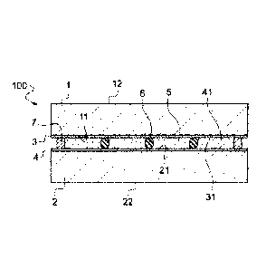
regard to the appended figure, Figure 1, which shows a
schematic cross-sectional view of a glazing unit having
CA 02890846 2015-05-07
- 28 -
liquid-crystal-mediated variable scattering properties with an
electrically conductive support according to the invention.
The example embodiment shown in Figure 1 shows the design
of the switchable liquid-crystal-comprising glazing unit
according to the invention.
Thin-film multilayers 3, 4 having external surfaces 31,
41 and containing electrodes made of indium tin oxide (ITO)
are deposited on the internal faces 11, 21 of two float-glass
(or as a variant on plastic such as PET) sheets 1 and 1'.
More precisely the multilayer comprises at least two thin
films acting as barriers to short-circuits, which films are
deposited on the ITO film, as will be described below.
Preferably, to ensure the colour neutrality of the
switchable glazing unit, the multilayer comprises at least two
thin dielectric underfilms under the ITO film, as will be
detailed below.
A liquid-crystal layer 5 is located between the
multilayers 3 and 4. More precisely, the liquid-crystal layer
is for example a PDLC layer and contains liquid crystals in
the form of microdroplets dispersed in a polymer matrix. The
layer 5 also contains spherical transparent polymer spacers.
The layer 5 is for example 20 pm in thickness and may
typically be 5 to 60 pm in thickness.
Liquid crystals such as the compound 4-((4-ethy1-2,6-
difluoropheny1)-ethiny1)-4'-propylbiphenyl or 2-fluoro-4,4'-
bis(trans-4-propylcyclohexyl)-biphenyl, for example sold by
Merck under the reference MDA-00-3506, may be used.
The edge of the liquid-crystal layer 5 is encircled by an
adhesive seal 7 made of a cured polymer that serves to join
. .
CA 02890846 2015-05-07
- 29 -
the electrode-bearing glass sheets 1, 1' both firmly and
permanently.
In the "OFF" state, i.e. before an electrical voltage has
been applied, this liquid-crystal-comprising glazing unit 100
is translucent, i.e. it transmits light but is not
transparent. Once a sinusoidal voltage has been applied
between the two electrodes, the layer 5 passes to the
transparent state, i.e. the state in which sight is no longer
obstructed.
Naturally, for certain applications, it may alternatively
be desired for the electrically controllable glazing unit to
be tinted in its "ON" state. To do this, one or the substrates
are tinted or a tinted element, for example a tinted plastic
film or a tinted counter pane is laminated with one of the
mineral glass substrates (by PVB, EVA, etc.), or a tinted
interlayer, is added.
EXAMPLES
In example Exl, the following multilayer: ITO (60
nm)/S13N4 (15 nm)/S102 (60 nm) was produced on a 4 mm-thick
sample of soda-lime-silica glass (Planilux glass from SGGF or
alternatively Diamant glass).
In example Ex2, the following multilayer: Si3N4 (15
nm)/S102 (30 nm)/ITO (60 nm)/Si3N4 (35 nm)/Si02 (48 nm) was
produced on a 4 mm-thick sample of soda-lime-silica glass
(Planilux glass from SGGF).
In example Ex3, the following multilayer: Si02 (40 nm)/ITO
(120 nm)/S13N4 (15 nm)/SiO2 (60 nm) was produced on a 4 mm-
thick sample of soda-lime-silica glass (Planilux glass from
SGGF).
CA 02890846 2015-05-07
- 30 -
In example Ex4, the following multilayer: Si3N4 (15
nm)/S102 (40 nm)/ITO (120 nm)/Si3N4 (15 nm)/Si02 (60 nm) was
produced on a 4 mm-thick sample of soda-lime-silica glass
(Planilux glass from SGGF).
In example Ex5, the following multilayer: Si3N4 (25
nm)/S102 (40 nm)/ITO (60 nm)/Si3N4 (35 nm)/Si02 (60 nm) was
produced on a 4 mm-thick sample of soda-lime-silica glass
(Planilux glass from SGGF).
More precisely, the silicon nitride film and the silica
film contained aluminium.
The films were deposited by sputtering (magnetron
sputtering). The deposition conditions for each of the films
were the following:
- films based on Si3N4:A1 were deposited by reactive
sputtering using a silicon and aluminium target in an
argon/nitrogen atmosphere;
- films based on Si02:A1 were deposited by reactive
sputtering using a silicon and aluminium target in an
argon/oxygen atmosphere; and
- films based on ITO were deposited using a ceramic
target, in an argon/oxygen atmosphere as a variant.
The deposition conditions are collated in Table 1 below:
Refractive
Target Deposition
Film Gas index at
employed pressure
550 nm
92:8 wt% 2x10 N2/ (Ari-N2)
Si3N4 :A1 2.0
Si:Al mbar of 40%
92:8 wt% 2x10
02/ (Ar+02)
Si02:Al 1.5
Si:Al mbar of 45%
CA 02890846 2015-05-07
- 31 -
90 wt% In
02 < 4%
oxide and 2.5x10⁻³
ITO and Ar > 2
wt% Sn mbar
96%
oxide
Table 1
The TL and sheet resistance of the electrically conductive
supports Exl to Ex4 are given in Table 2 below:
Examples Re (Q/0) TL(%)
Exl 91 88.0
Ex2 140 88.8
Ex3 117 87.0
Ex4 105 87.3
Ex5 105 88.0
Table 2
The short-circuit yield Rcc, which is the percentage of 1
m2 of liquid-crystal-comprising glazing unit free from short-
circuits after switching at the indicated voltage, was
measured for the glazing units having liquid-crystal-mediated
variable scattering properties of examples Exl to Ex4.
In the series of tests carried out, Rcc was near 100% at
30 V and greater than 70% at 90 V compared to 40% and 0% for a
glass sample coated with an ITO film, and compared to 70% and
0% when a 60 nm-thick Si02 film was applied.
TL and other optical properties were also measured for the
liquid-crystal-comprising glazing units (LC glazing or LCG) in
the ON state, the measured values being collated in Table 3
below:
CA 02890846 2015-05-07
- 32 -
Example TL L*T a*T b*T RL L*R a*R b*R abp
LCG of
73.9 88.9 -1.3 0.5 20.2 52.0 -3.7 6.2 6.0
Exl
LCG of
83.7 93.3 -3.5 6.3 9.5 36.9 2.9 -5.0 6.8
Ex2
LCG of
81.2 92.2 -4.2 15.2 10.4 38.5 3.7 -21.5 8.4
Ex3
LCG of
81.9 92.5 -4.9 12.3 9.7 37.3 6.8 -14.3 9.7
Ex4
Table 3
The LC glazing units of Exl and Ex2 had a neutral colour
in reflection: a* and b* were in the -8, +8 interval.
The LC glazing unit of Ex4 was grey-blue (neutral but
bright colour) and the LC glazing unit of Exl was green.
As a variant, a third 20 nm-thick barrier film made of
zinc tin oxide and produced from a metal zinc/tin target in an
oxidizing atmosphere is placed intermediate between the first
and second barrier films. The deposition conditions are given
in Table 4 below:
Refractive
Target Deposition
Film Gas index at
employed pressure
550 nm
SnZnO 64:36 wt% 3.5x10⁻³ 02/ (Ar+02)
2
Sn:Zn mbar of 39%
Table 4
CA 02890846 2015-05-07
- 33 -
As a (alternative or cumulative) variant, a 5 nm-thick
protective film made of titanium oxide produced from a metal
target in an oxidizing atmosphere is added onto the second
barrier film. This film has the effect of improving mechanical
properties. The deposition conditions are detailed in Table 5
below:
Refractive
Target Deposition
Film Gas index at
employed pressure
550 nm
TiO2 Ti 2.5x10 02/ (Ar+02)
2.5
mbar of 10%
Table 5
Another TCO could be used, preferably deposited by
sputtering, with the same barrier films and preferably
neutralizing films as used above.
For optical reasons, it is preferable for the last
barrier film to be based on silicon oxide and for it to be the
second barrier film.