Note : Les descriptions sont présentées dans la langue officielle dans laquelle elles ont été soumises.
CA 02891017 2015-05-07
273471-2
CALIBRATION METHODS FOR VOLTAGE SENSING DEVICES
BACKGROUND
[0001] Embodiments of the present specification relate to voltage sensing
devices,
and more particularly to calibration methods for the voltage sensing devices.
[0002] Recently, deregulation of the electricity supply market has led to
increased
competition between electricity providers. It is now relatively common for
companies
and households to have a choice of several different electricity providers
when deciding
on an electricity provider to supply their electricity needs. This has led to
competition
between the different providers over matters including pricing and quality of
supply.
Further, sometimes electricity providers need to supply their customers with
less
expensive electricity while still assuring the same or improved quality of
supply to their
customers. In order to achieve these goals the electricity providers have to
improve the
efficiency of electricity networks or electricity distribution system.
Furthermore, due to
deregulation, network losses and interruption to electricity supply are now
being
penalized.
[0003] Typically, it has been found that even in highly developed
countries,
approximately 10% of all electricity generated is lost within the electricity
networks
themselves. For example, a portion of the electricity being transmitted
through a current
carrying cable, also referred to as a "power line" of an electricity network
may be lost as
a result of transmission losses. This figure representing electricity loss
within the
electricity network rises to almost 25% in less developed nations. This loss
of power in
the electricity network may be due to undetected faults. Further, these faults
may go
undetected for long periods of time. Moreover, even when the faults are
detected, it is
usually challenging to locate the faults over an expansive electricity
network. By
providing the information of the electrical properties in the electricity
network (e.g., by
monitoring the electricity networks) in an accurate manner, electricity
providers may be
1
CA 02891017 2015-05-07
273471-2
able to significantly reduce the amount of electricity lost in the electricity
networks and
make considerable savings in the cost of generating the electricity.
Furthermore, by
closely monitoring the electricity networks electricity providers will be in a
better
position to correct faults in the electricity networks swiftly with a minimum
of
inconvenience to their customers, thereby providing an improved quality of
supply to
their customers.
[0004] A variety of sensors have been developed for measuring a current in
a current
carrying cable, such as a current carrying cable in a high voltage electricity
distribution
system. For example, optical current sensors are used to measure the current
in the
current carrying cable. The opticp1 current sensors are generally based on the
Faraday
effect. Some optical current sensors use bulk glass or fiber optic cables that
surround the
current carrying cable. Although the optical current sensors have a very high
dynamic
range, however, the optical current sensors require opening the current
carrying cable at
installation, which may be an expensive procedure.
[0005] Other kind of sensors that are used for measuring voltages in the
electricity
networks may employ metal shells disposed around the current carrying cables.
These
sensors use the metal shells as capacitance dividers between the current
carrying cables
and a ground underneath. Among other factors, the capacitance between the
shells and
the current carrying cables depends on the distance between the shells and the
current
carrying cables. Accordingly, the metal shells may have limited capacitance
between the
current carrying cables and the shells themselves because of a limit on a gap
between the
shells and the current carrying cables. Further, due to the limited
capacitance, the sensor
may be influenced by changes in surrounding conductors, such as measuring
circuits.
Moreover, an increase in an area of the shell to increase a capacitance
between the shells
and the current carrying cables typically results in an increase in a
parasitic capacitance
of the sensor. The increased parasitic capacitance makes the sensor relatively
more prone
to fluctuations in the surrounding conductors.
2
CA 02891017 2015-05-07
273471-2
[0006] Further, in case of sensors configured to measure voltage values in
the power
line, the voltage measurement entails physically connecting the voltage
measuring device
to the voltage line and to the ground. This physical connection between the
voltage
measuring device and the ground is required to prevent monitored values being
undesirably affected by the presence of any object that may exist between the
ground and
the voltage measuring device. By way of example, a passing vehicle, a tree, an
animal, or
a bird, or any other object intentionally or unintentionally disposed in close
vicinity of the
ground and/or the voltage measuring device may result in undesirable changes
in the
measurement values of the voltage measurement device in absence of the
physical
connection between the voltage measuring device and the ground. It may be
noted that
providing this physical connection between the voltage measuring devices and
the ground
requires complex installation procedures. For example, such installation
procedures are
both time consuming and labor intensive resulting in an increase in the cost
of installing
the voltage measuring device. Further, the physical connection to the ground
may need
to be maintained and periodically checked.
BRIEF DESCRIPTION
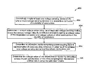
[0007] In accordance with aspects of the present specification, a
calibration method
for enhancing a measurement accuracy of one or more voltage sensing devices in
presence of a plurality of conductors is provided. The method includes
operatively
coupling at least one voltage sensing device of the one or more voltage
sensing devices to
a respective conductor of the plurality of conductors and determining a sensed
voltage
value of the respective conductor using the at least one voltage sensing
device The
method further includes determining a calibration matrix having cross-coupling
factors
representative of cross-coupling between an antenna of the at least one
voltage sensing
device and other conductors of the plurality of conductors and determining a
corrected
voltage value of the respective conductor by deducting at least in part
contributions of the
cross-coupling from the sensed voltage value of the respective conductor using
the
calibration matrix.
3
CA 02891017 2015-05-07
273471-2
[0008] In accordance with another aspect of the present specification, a
method for
determining individual voltage values of one or more power lines of multi-
phase power
lines is provided. The method includes operatively coupling respective
contactless
voltage sensing devices to one or more power lines of the multi-phase power
lines.
Further, each of the respective contactless voltage sensing devices includes a
first
impedance element having a first impedance, where the first impedance element
is
configured to be operatively coupled to a respective power line of the one or
more power
lines, an antenna operatively coupled to the first impedance element, a second
impedance
element having a second impedance, and measurement and communication circuitry
operatively coupled to the first impedance element. Moreover, the second
impedance
element is formed in part by the antenna and a parasitic impedance element,
and where
the parasitic impedance element includes a parasitic impedance. The method
further
includes determining sensed voltage values for the one or more power lines of
the multi-
phase power lines using the respective contactless voltage sensing devices.
Additionally,
the method includes determining a calibration matrix comprising cross-coupling
factors,
where the cross-coupling factors are representative of cross-coupling between
the
respective contactless voltage sensing devices and other power lines of the
multi-phase
power lines. Also, the method includes determining the individual voltage
values of the
respective power lines by deducting at least in part contributions of the
cross-coupling
from the sensed voltage values using the calibration matrix.
[0009] In accordance with yet another aspect of the present specification,
a
monitoring system having a plurality of conductors, a plurality of contactless
voltage
sensing devices, and a monitoring unit is provided. The monitoring unit is
operatively
coupled to one or more contactless voltage sensing devices of the plurality of
contactless
voltage sensing devices and configured to determine voltage values of the
respective
conductor of the plurality of conductors.
4
CA 02891017 2015-05-07
273471-2
DRAWINGS
[0010] These and other features, aspects, and advantages of the present
specification
will become better understood when the following detailed description is read
with
reference to the accompanying drawings in which like characters represent like
parts
throughout the drawings, wherein:
[0011] FIG. 1 is a schematic representation of an exemplary contactless
voltage
sensing device having an electrically conductive housing, in accordance with
aspects of
the present specification;
[0012] FIG. 2 is a schematic representation of an exemplary contactless
voltage
sensing device having an electrically conductive shield, in accordance with
aspects of the
present specification;
[0013] FIG. 3 is a schematic representation of an exemplary contactless
voltage
sensing device having an antenna, where at least a portion of the antenna is
electrically
insulated, in accordance with aspects of the present specification;
[0014] FIG. 4 is a schematic representation of an exemplary monitoring
system
employing a contactless voltage sensing device, in accordance with aspects of
the present
specification;
[0015] FIG. 5 is a schematic representation of cross-coupling between
respective
antennae of contactless voltage sensing devices and neighboring conductors of
the
contactless voltage sensing devices, in accordance with aspects of the present
specification; and
[0016] FIG. 6 is a flow chart for an exemplary method for installing and
calibrating a
contactless voltage sensing device, in accordance with aspects of the present
specification.
CA 02891017 2015-05-07
273471-2
DETAILED DESCRIPTION
[0017] Embodiments of the present specification provide calibration methods
for
enhancing a sensing capability of one or more voltage sensing devices in
presence of a
plurality of conductors. Usually, when an electrical current flows through a
conductor or
the conductor is electrically charged, the conductor produces an
electromagnetic field.
This electromagnetic field of the conductor is typically proportional to
electrical
parameters (e.g., a voltage and/or current) of the conductor. Further,
electromagnetic
fields from one or more conductors present in a neighborhood of the conductor
may
undesirably influence sensed voltage values of the voltage sensing devices.
Accordingly,
the sensed voltage value of a given conductor may be contributed at least in
part by a
voltage value of the given conductor as well as voltage values of other
conductors of the
plurality of conductors.
[0018] This phenomenon of the voltage sensing devices being influenced by
the
electromagnetic fields of the conductors present in the neighborhood in
addition to being
effected by the electromagnetic fields of a conductor on which the voltage
sensing device
is mounted may be referred to as "cross-coupling." Further, it may be
desirable to deduct
at least in part or nullify the effect of the cross-coupling from the sensed
voltage values to
obtain a corrected voltage value of the conductor.
[0019] In certain embodiments, the cross-coupling may occur between a
voltage
sensing device and another conductor of a plurality of conductors. In
particular, the
cross-coupling may occur between the voltage sensing device and the other
conductor
when an electromagnetic field of the other conductor interferes or interacts
with the
voltage sensing device of the conductor. In certain embodiments, where the
voltage
sensing devices are contactless voltage sensing devices, one or more
conductors of the
plurality of conductors may employ respective one or more contactless voltage
sensing
devices. Further, in some of these embodiments the cross-coupling may exist
between a
given contactless voltage sensing device of a respective conductor of the
plurality of
conductors and other conductors of the plurality of conductors. These other
conductors
6
CA 02891017 2015-05-07
273471-2
may be referred to as neighboring conductors. This cross-coupling between the
contactless voltage sensing device and the neighboring conductors may
undesirably affect
a sensed voltage value of the given contactless voltage sensing device.
Accordingly, it is
desirable to at least partly remove the effect of the cross-coupling from the
sensed voltage
value of the given contactless voltage sensing device to obtain a voltage
value of the
respective conductor. Advantageously, the voltage value of the conductor thus
obtained
is a relatively more accurate representation of the voltage value of the
conductor.
[0020] As used throughout the present specification, the term "conductor"
refers to an
electrical conductor. As used herein, the term "contactless" refers to absence
of direct
physical contact between the contactless voltage sensing device and a
reference surface,
and other conductors (e.g., other transmission lines in multi-phase
transmission). In a
particular example, the contactless voltage sensing device of the present
specification
may not be directly physically coupled to the ground to provide the reference
potential. It
may be noted that in some embodiments the reference surface may be a ground or
a
neutral conductor. However, in some other embodiments, the reference surface
may be
any other surface other than the ground, where the reference surface has a
known
potential, referred to as a "reference potential."
[0021] In certain embodiments, the calibration methods may be used to
reduce effects
of cross-coupling between corresponding antenna of the one or more contactless
voltage
sensing devices and neighboring conductors of the plurality of conductors.
Further, the
calibration methods may be used to reduce effects of parasitic impedances to
further
enhance the sensing capability of on an accuracy of the one or more
contactless voltage
sensing devices. In one example, each conductor of the plurality of conductors
may be
coupled to a respective contactless voltage sensing device. However, in
another example,
one or more conductors of the plurality of conductors may not be coupled to a
contactless
voltage sensing device.
[0022] In one example, the calibration methods may be used to at least
partly reduce
or nullify the effects of the cross-coupling between the contactless voltage
sensing
7
CA 02891017 2015-05-07
273471-2
devices and multi-phase power lines. In a particular example, the multi-phase
power
lines may be three-phase distribution lines. Further, the multi-phase power
lines may be
a part of distribution network for electricity supply. As used herein, the
terms
"distribution line," "transmission line" and "power line" may be used
interchangeably
throughout the present specification.
[0023] In operation, the electromagnetic field that exists around a power
line when
the current flows through the power line may undesirably influence electronic
components disposed in a surrounding environment of the power line.
Accordingly, in
case of multi-phase power lines, when each power line of the multi-phase power
lines
employs one or more contactless voltage sensing devices, each contactless
voltage
sensing device may be influenced by the electromagnetic field of the other
power lines of
the multi-phase power lines. By way of example, in case of three-phase power
lines,
where each of the three-phase power lines have a respective contactless
voltage sensing
device, the voltage value measured by each of the contactless voltage sensing
devices
may reflect a contribution from the three power lines, and not just from the
respective
power line to which the contactless voltage sensing device is coupled to
measure the
voltage value. Accordingly, it is desirable to measure an effect of the
electric field
generated by each power line on a voltage sensing device that is operatively
coupled to a
neighboring power line to facilitate calculation of a corrected voltage value
of the power
line. The methods of the present specification may be used for existing as
well as future
voltage sensing devices.
[0024] In certain embodiments, the contactless voltage sensing devices may
be
preferred due to ease of installation. By way of example, in case of the
contactless
voltage sensing devices it is not required to provide a physical contact
between the
sensing device and the ground. Accordingly, mounting the contactless voltage
sensing
device primarily entails physically coupling the contactless voltage sensing
device on the
body configured to carry current. For example, in case of the conductor being
a power
line, the contactless voltage sensing device may be clamped on to the power
line.
8
CA 02891017 2015-05-07
273471-2
Further, advantageously, the contactless voltage sensing device is not
influenced by
presence or absence of physical objects between the ground and the sensor.
Hence, it
may be desirable to use the contactless voltage sensing devices. Further,
since the
contactless voltage sensing device is operatively coupled to a single power
line of multi-
phase power lines, hence, the contactless voltage sensing device does not
interfere with
the structure or the or layout of the power lines.
[0025] In certain embodiments, the contactless voltage sensing device may
include a
first impedance element having a first impedance and a second impedance
element
having a second impedance. The first and second impedances may be used to
measure
the voltage of the conductor. Non-limiting examples of the first impedance
element may
include one or more resistors, one or more capacitors, one or more inductors,
or
combinations thereof. In one example, the contactless voltage sensing device
may
include a capacitor as the first impedance element. In operation, the first
impedance
element is configured to sense an electrical parameter, such as the voltage of
the
conductor.
[0026] Further, the contactless voltage sensing device includes an antenna
that is
operatively coupled to the first impedance element. The antenna is configured
to form
the second impedance element in conjunction with the parasitic impedance
element. In
particular, the second impedance element is formed by the antenna and a
parasitic
impedance element, where the parasitic impedance element is formed between the
antenna and the reference surface. An impedance of the second impedance
element, also
referred to as "second impedance," is a combination of an impedance of the
parasitic
impedance element, also referred to as "parasitic impedance," and an impedance
of the
antenna. Further, due to design of the contactless voltage sensing device, in
some
embodiments, the impedance of the antenna may be negligible compared to the
parasitic
impedance. In these embodiments, a value of the second impedance may be
substantially
similar to a value of the parasitic impedance. Accordingly, the second
impedance may be
substantially a parasitic impedance that appears between the antenna and the
reference
9
CA 02891017 2015-05-07
273471-2
surface. In a non-limiting example, the parasitic impedance may primarily
include a
parasitic capacitance.
[0027] Further, in
certain embodiments, the contactless voltage sensing device
includes measurement and communication circuitry, where the measurement and
communication circuitry is configured to measure a voltage of the conductor
based on the
voltage value sensed across the first impedance element. Further, in
certain
embodiments, the first impedance element may be disposed between a first node
and a
second node. Similarly, the antenna may be disposed between another first node
and
another second node. Moreover, the second node of the first impedance element
may be
operatively coupled to the first node of the antenna. In a particular example,
the second
node of the first impedance element and the first node of the antenna may be a
common
node between the first impedance element and the antenna. In operation, the
first node of
the first impedance element may be maintained at the same potential as that of
the
conductor. Maintaining the first node of the first impedance element at the
same
potential as that of the conductor enables the contactless voltage sensing
device to
measure the voltage of the conductor by enabling a voltage corresponding to
the
conductor to appear across the first impedance element. Further, the second
node of the
antenna may be configured to develop a voltage that is different from the
voltage of the
conductor. The voltage appearing on the second node of the antenna may be
caused due
to a current flowing through the parasitic impedance element. Consequently,
the
structure of the contactless voltage sensing device enables the combination of
the first
and second impedance elements to act as a voltage divider between the
conductor and the
reference surface. Due to this voltage division between the first and second
impedance
elements a voltage difference may be created across the first impedance
element.
Further, the measurement and communication circuitry may be configured to
measure
this voltage difference appearing across the first impedance element. In
some
embodiments, the measurement and communication circuitry may be configured to
measure the voltage of the conductor based on the values of the first
impedance, second
impedance and voltage difference appearing across the first impedance element.
CA 02891017 2015-05-07
273471-2
[0028] In certain embodiments, the contactless voltage sensing device
includes an
electrically conductive element configured to shield the first impedance
element from
electromagnetic radiation emanating from the conductor, such as a current
carrying
power line. Further, in some embodiments, the electrically conductive element
may be
maintained at the same voltage as that of the conductor.
[0029] Moreover, it may be noted that the antenna may be an electrically
conductive
body that has a first portion and a second portion. Further, an electrical
insulator may be
disposed on the first portion of the antenna to prevent electrical shorting of
the
electrically conductive body of the antenna with the electrically conductive
element.
Additionally, the second portion of the antenna may be disposed outside the
electrical
insulator as well as the electrically conductive element. The second portion
of the
antenna that is disposed outside the electrical insulator as well as the
electrically
conductive element may be exposed to the reference surface. Further, the
second portion
of the antenna in conjunction with the reference surface may contribute to
formation of
the second impedance and/or parasitic impedance. In certain embodiments,
dimensions
of the second portion of the antenna may be selected to facilitate relatively
smaller values
of antenna impedance as compared to parasitic impedance. The second portion of
the
antenna acts as the second node of the antenna.
[0030] In certain embodiments, the contactless voltage sensing device may
be
configured to communicate the measured voltage value to a determined location,
such as,
but not limited to, a control unit, a monitoring unit, a display unit, or
combinations
thereof. Further, the contactless voltage sensing device may be configured
to
communicate the measured voltage value using the measurement and communication
circuitry. Advantageously, the contactless voltage sensing device may be
configured to
enable real-time monitoring of the voltage values of the conductor, such as,
but not
limited to, a power line.
[0031] Advantageously, measurement values of the contactless voltage
sensing
device are not undesirably or adversely affected by presence or absence of
electrically
11
CA 02891017 2015-05-07
273471-2
conductive or electrically non-conductive objects that may be intentionally or
unintentionally disposed between the contactless voltage sensing device and
the reference
surface while the contactless voltage sensing device is sensing and measuring
the voltage
values of the power line on which it is disposed. By way of example, the
measured
voltage value of a power line measured by the contactless voltage sensing
device may not
be adversely affected due to presence of an electrically conducting body, such
as, but not
limited to, a stationary or moving vehicle in the vicinity of the power line.
Further, the
contactless voltage sensing device is relatively easy to install as compared
to
conventional measurement devices that require a direct physical connection
between the
measurement device and the ground. In particular, the contactless voltage
sensing device
is configured to be mounted on the power line without any further need of the
contactless
voltage sensing device being physically coupled to the ground.
[0032] Additionally, one or more contactless voltage sensing devices may be
configured to be employed in a monitoring system, where the monitoring system
may
include the control unit and/or the monitoring unit. The one or more
contactless voltage
sensing devices may be configured to communicate the measured voltage values
of the
conductor to the control unit and/or the monitoring unit. In some embodiments,
the one
or more contactless voltage sensing devices may include a plurality of data
acquisition
communicators (DACs). In some embodiments, the DACs may form part of the
measurement and communication circuitry. In certain embodiments, data
representative
of the voltage of the power line is communicated by a DAC to the control unit,
such as
the control center computer, over a global system for mobile communication
(GSM) link.
This is an inexpensive and secure way of sending the data to the control unit,
the
monitoring unit, or any other control center computer or device.
[0033] Moreover, in some embodiments, the monitoring system may form part
of an
electricity network. Further, the electrical network may employ one or more
monitoring
systems. In some of these embodiments, the electricity network may employ a
plurality
of power lines, a plurality of contactless voltage sensing devices, and one or
more
12
CA 02891017 2015-05-07
273471-2
monitoring systems. Further, one or more contactless sensing devices of the
plurality of
contactless voltage sensing devices may be operatively coupled to one or more
monitoring systems. In one example, the monitoring system may be configured to
communicate the measured voltage values to a control unit in the electricity
network. In
certain embodiments, the contactless voltage sensing devices may be configured
to
provide signals representative of the voltage value of a corresponding power
line of the
electricity network over a wide geographical area in a cost effective way. In
one
embodiment, each DAC of the plurality of DACs may have one or more contactless
voltage sensing devices associated therewith so that the signals
representative of the
voltage values of the power lines may be transmitted from a contactless
voltage sensing
device to another contactless voltage sensing device or the control unit of
the same or the
other monitoring systems. In one example, the electrical properties
transmitted from one
DAC to the control unit may be transmitted to another DAC before being
transferred to
the control unit. By having a plurality of DACs, processing may be carried out
either at
the DACs or in the control unit. In one example, the signals may be amplified
in the
DAC and temporary storage of the data may be carried out in each DAC.
[0034] Further, the contactless voltage sensing device of the present
specification
may be easily adaptable to different dynamic ranges, bandwidths and
sensitivity values.
In one embodiment, the first impedance element may be modified to adapt the
contactless
voltage sensor for the different dynamic ranges, bandwidths and sensitivity
values. By
way of example, in instances where the first impedance element is a capacitor,
a capacitor
with higher capacitance may be used to obtain lower bandwidth, and vice versa.
In one
embodiment, a value of the first capacitance of the first impedance element
may be equal
to or more than about 1 nF. In the same or different embodiment, a value of
the parasitic
capacitance from the second impedance element may be less than or equal to
about
0.01pF.
[0035] FIG. 1 illustrates an exemplary contactless voltage sensing device
100. The
contactless voltage sensing device 100 may be configured to measure a voltage
value of a
13
CA 02891017 2015-05-07
273471-2
conductor, such as, but not limited to, a power line 102 with respect to a
reference surface
120. The power line 102 may be a high voltage line, a medium voltage line, or
any other
power line or any other electrical conductor that is configured to carry
electrical current.
In certain embodiments, the contactless voltage sensing device 100 includes an
electrically conductive element in the form of an electrically conductive
housing 104.
The electrically conductive housing 104 may be configured to shield one or
more
components of the contactless voltage sensing device 100 from electromagnetic
radiation
of the power line 102. Further, the electrically conductive housing 104 may
provide
shielding to one or more sides of the contactless voltage sensing device 100.
In some
embodiments, the electrically conductive housing 104 may be maintained at the
same
voltage as the power line 102. In one embodiment, the electrically conductive
housing
104 may be shunted to the power line 102 using an electrically conductive
connector 106.
Maintaining the electrically conductive housing 104 at the same potential as
the power
line 102 may facilitate reduction in interference otherwise caused due to
presence of the
electrical field around the electronic components of the contactless voltage
sensing device
100. Further, maintaining the electrically conductive housing 104 at the same
potential as
that of the power line 102 enhances accuracy of measurement of the contactless
voltage
sensing device 100.
[0036] In the
illustrated embodiment, the contactless voltage sensing device 100
further includes a first impedance element 108 disposed between a first node
107 and a
second node 109. In some embodiments, the first impedance element 108 may
include a
capacitor, a resistor, an inductor, or combinations thereof. Further, the
first impedance
element 108 may have an impedance that is referred to as a "first impedance,"
hereinafter. The first impedance element 108 is configured to sense at least
one electrical
parameter of the power line 102. By way of example, a voltage appearing across
the first
impedance element 108 is representative of the sensed electrical parameter of
the power
line 102. The first impedance element 108 is connected to the power line 102
at the first
node 107.
14
CA 02891017 2015-05-07
273471-2
[0037] Further, the first impedance element 108 is operatively coupled to
an antenna
110 at the second node 109. The second node 109 is a common node shared
between the
first impedance element 108 and the antenna 110. Further, the voltage
appearing across
the first impedance element 108 is representative of the voltage difference
that exists
between the power line 102 and the second node 109. In embodiments where the
electrically conductive housing 104 is maintained at the same voltage as that
of the power
line 102, the voltage difference between the power line 102 and the second
node 109 is
the same as the voltage difference between the electrically conductive housing
104 and
the second node 109. Accordingly, the voltage difference across the first
impedance
element 108 may be measured by disposing a voltage sensing device, such as a
voltmeter
112, between nodes 114 and 116.
[0038] Further, the antenna 110 includes a first portion 130 and a second
portion 131.
It may be noted that the first and second portions 130 and 131 of the antenna
110 may not
be physically different entities. The first portion 130 of the antenna 110 may
be the
portion of the antenna 110 that is insulated from the electrically conductive
housing 104
using an electrical insulator 128. Further, the second portion 131 of the
antenna 110 may
be the portion that is disposed outside the electrical insulator 128. Further,
the second
portion 131 of the antenna 110 may be disposed outside the electrically
conductive
housing 104. Further, the second portion 131 of the antenna 110 may be exposed
to the
reference surface 120, generally represented by a node 124. In certain
embodiments, the
node 122 of the antenna 110 is formed on the second portion 131 of the antenna
110. In
particular, the antenna 110 is disposed between the node 109, which is the
first node of
the antenna 110 and a node 122, which is the second node of the antenna 110.
Further,
the second portion 131 of the antenna 110 is exposed outside the electrical
insulator 128.
[0039] In the illustrated embodiment, the contactless voltage sensing
device 100
includes a second impedance element 133 that is formed by at least a portion
of the
antenna 110 and a parasitic impedance element 118. In particular, the second
impedance
element 133 is formed by the second portion 131 of the antenna 110 and the
parasitic
CA 02891017 2015-05-07
273471-2
impedance element 118. Further, the parasitic impedance element 118 is
disposed
between the antenna 110 and the reference surface 120. In particular, the
parasitic
impedance element 118 exists between the node 122 of the antenna 110 and the
node 124
representative of the reference surface 120. An impedance value of the second
impedance element 133 may be referred to as a second impedance. It may be
noted that
the second impedance is a combination of a parasitic impedance and an
impedance of the
antenna. Further, it may be noted that the second impedance may be
substantially similar
to the parasitic impedance as a value of the impedance of the antenna may be
substantially lower compared to a value of the parasitic impedance.
[0040] Further, in embodiments where the reference surface is a ground, the
parasitic
impedance may be defined as the parasitic capacitance between the antenna 110
and the
ground. However, in other embodiments where the reference surface 120 is a
surface
different from the ground, the parasitic capacitance may be defined as an
impedance
between the antenna 110 and a reference potential, where the reference
potential is a
potential of the reference surface 120.
[0041] Additionally, in embodiments where at least a portion of the antenna
110 is
disposed in the electrical insulator 128, the overall size of the antenna 110
may not
matter, however, only the second portion 131 of the antenna that is disposed
outside the
electrical insulator 128 may contribute to the parasitic impedance. In some
embodiments,
a length of the second portion 131 may be up to about 10 cm. Accordingly, it
may be
desirable to provide the antenna 110 having relatively small dimensions of the
second
portion 131 to provide relatively high parasitic impedance for the parasitic
impedance
element. It may be noted that high parasitic impedance or low parasitic
capacitance
enables the contactless voltage sensing device to be not undesirably
influenced by
changes in surrounding conductors. Consequently, the increased parasitic
impedance
renders the contactless voltage sensing device 100 relatively less prone to
fluctuations in
the surrounding conductors while still maintaining physical separation between
the
contactless voltage sensing device 100 and the reference surface 120. Further,
in some
16
CA 02891017 2015-05-07
273471-2
embodiments, the antenna 110 may be a cable, a wire, a plate, a patterned
elongated
structure, an impedance element, or combinations thereof. In one embodiment,
the
antenna 110 may include a lumped impedance element. By way of example, the
antenna
110 may be a lumped capacitor, where a first terminal of the capacitor is
disposed in the
electrical insulator 128 and a second terminal of the lumped capacitor is
exposed to the
reference surface 120.
[0042] Further, it may be noted, that the voltage difference (Vi) between
the nodes
107 and 109 of the first impedance element 108 may appear primarily because of
the
impedance divider action caused due to the presence of the antenna 110 between
the first
impedance element 108 and the reference surface 120. In particular, presence
of the
antenna 110 results in the formation of the second impedance element 133,
thereby
providing the divided impedance. In one example where the antenna impedance is
assumed to be negligible compared to the parasitic impedance, and where the
first
impedance element 108 is a capacitor, the antenna 110 may result in the
formation of the
parasitic capacitor. Further, in this example, the first impedance element 108
or the
capacitor may act as a voltage divider between the power line 102 and the
reference
surface 120.
[0043] In one embodiment, the second impedance may be at least about 50
times
higher than the value of the first impedance. In another embodiment, the
second
impedance may be at least about 100 times higher than the value of the first
impedance.
In yet another embodiment, the second impedance is about 100 to 10,000 times
higher
than the value of the first impedance. In some embodiments, the second
impedance may
have a relatively high value by virtue of having a high parasitic impedance, a
high
antenna impedance, or both. In some other embodiments, the second impedance
may
have a relatively high value by virtue of having a high parasitic impedance.
While the
value of the first impedance is primarily governed by the type of device that
is used as the
first impedance element, the parasitic impedance is primarily governed by the
size of the
antenna 110. Further, the value of the antenna impedance may be governed by
the
17
CA 02891017 2015-05-07
273471-2
impedance element used to form the antenna 110. In order to have a relatively
low value
for the first impedance, in some embodiments, a lumped capacitor may be used
as the
first impedance element 108.
[0044] In some
embodiments, the voltage in the power line 102 may be calculated
using the value of the first impedance, second impedance, and the voltage
difference
across the first impedance element 108. The voltage of the power line may be
represented by Equation (1)
Equation (1)
L= __ *vo
where VL represents voltage of the power line 102 with respect to reference
surface 120,
Vo represents voltage difference across the first impedance element, Z1
represents the first
impedance value, and Z2 represents the second impedance value. The voltage
value
across the first impedance element 108 may be governed by the voltage of the
power line
102, however, the value of the second impedance may be governed by the antenna
impedance, size of the antenna 110 disposed outside the electrical insulator
128, and the
distance between the antenna 110 and the reference surface 120. It is
desirable to have
minimum variation in the value of the parasitic impedance. Due to the small
size of the
antenna 110, the value of the parasitic impedance is relatively high.
Hence,
advantageously, the variation in the estimated value of the voltage (VL) of
the power line
102 is minimized. Accordingly, presence of conductors or other objects between
the
contactless voltage sensing device 100 and the ground 120 does not adversely
affect the
measurement of the voltage values in the power line 102.
[0045] In certain
embodiments, the output of the voltmeter 112 may be operatively
coupled to measurement and communication circuitry 132. In some embodiments,
the
measurement and communication circuitry 132 may include a processor 134, a
monitor
136 and a DAC 138. The measurement and communication circuitry 132 is
configured to
measure the voltage difference across the first impedance element 108.
Further, the
processor 134 of the measurement and communication circuitry 132 is configured
to
determine a voltage value of the power line 102 based on the value of the
first impedance,
18
CA 02891017 2015-05-07
273471-2
a value of the voltage appearing across the first impedance element 108 and
the value of
the second impedance. Further, the determined value of the corrected voltage
of the
power line 102 may be wirelessly communicated to other contactless voltage
sensing
devices (not shown) or a control unit using the DAC 138
[0046] Also, the functions of the processor 134 may be implemented in a
variety of
programming languages, including but not limited to Ruby, Hypertext Pre-
processor
(PHP), Per!, Delphi, Python, C, C++, or Java. Such code may be stored or
adapted for
storage on one or more tangible, machine-readable media, such as on data
repository
chips, local or remote hard disks, optical disks (that is, CDs or DVDs), solid-
state drives,
or other media, which may be accessed by the processor-based system to execute
the
stored code.
[0047] In one embodiment, the measurement and communication circuitry 132
may
be a high input impedance circuitry. The measurement and communication
circuitry 132
may be configured to use the values of the first impedance and the parasitic
impedance to
determine the corrected voltage value of the power line 102. In the
illustrated
embodiment, the measurement and communication circuitry 132 may be disposed in
the
electrically conductive housing 104. However, in an alternate embodiment not
illustrated
here, the measurement and communication circuitry 132 may be disposed outside
the
electrically conductive housing 104.
[0048] The measurement and communication circuitry 132 is communicatively
coupled to other devices, such as a control unit (not shown), or other
contactless voltage
sensing devices using the DAC 138. In one embodiment, the control unit may be
configured to receive data representative of the voltage value of the power
line 102 from
the one or more contactless sensing devices 100.
[0049] In some embodiments, the measurement and communication circuitry 132
may be configured to provide a determined voltage value of the power line 102
to the
control unit. In one embodiment, the measurement and communication circuitry
132 may
19
CA 02891017 2015-05-07
273471-2
be configured to communicate with the control unit using a DAC 138 or a radio
transmitter/receiver. In certain embodiments, the contactless voltage sensing
device 100
may be a remote sensing device. The term "remote sensing device" may be used
to refer
to a sensing device that is communicatively coupled to a monitoring unit
and/or a control
unit while being located in a remote location with respect to the monitoring
unit and/or
the control unit. In one embodiment, the remote sensing device may be
wirelessly
coupled to the monitoring unit and/or the control unit.
[0050] Moreover, although not illustrated, the contactless voltage sensing
device 100
may include a protective cover or casing that is disposed around at least a
portion of the
electrically conductive housing 104. The protective cover may be made of
electrically
non-conductive materials, such as but not limited to, electrically non-
conductive
polymers or electrically non-conductive ceramics. Further, in one embodiment,
the
protective cover may be configured to provide mechanical strength and/or
environmental
protection to the contactless voltage sensing device 100.
[0051] FIG. 2 illustrates an alternate embodiment of the contactless
voltage sensing
device 100 of FIG. 1. In the illustrated embodiment, the contactless voltage
sensing
device 200 is operatively coupled to a power line 208 and configured to
measure a
voltage of the power line 208. The contactless voltage sensing device 200
includes a first
impedance element 202, an antenna 204 and measurement and communication
circuitry
206. The contactless voltage sensing device 200 may be configured to be
mounted on the
power line 208. Further, the contactless voltage sensing device 200 may
include an
electrically conductive element in the form of an electrically conductive
shield 210. The
electrically conductive shield 210 includes a first portion, namely a first
electrically
conductive shield 212, and a second portion, namely a second electrically
shield 214.
The first electrically conductive shield 212 of the electrically conductive
shield 210 is
disposed between the first impedance element 202 and the power line 208.
Accordingly,
the first electrically conductive shield 212 is configured to shield the
contactless voltage
sensing device 200 from the electromagnetic radiation from the power line 208.
Further,
CA 02891017 2015-05-07
273471-2
the second electrically conductive shield 214 of the electrically conductive
shield 210 is
disposed between the antenna 204 and a reference surface 216. The second
electrically
conductive shield 214 is configured to prevent any electrical interference
between the
reference surface 216 and the first impedance element 202. Further, the second
electrically conductive shield 214 may be configured to enable the formation
of a second
impedance element 225. In particular, the second impedance element 225 may be
formed
in part by the antenna 204 and a parasitic impedance element 218. Further, the
parasitic
impedance element 218 may be disposed between the antenna 204 and the
reference
surface 216.
[0052] Further, the antenna 204 includes a first portion 220, a second
portion 224 and
an electrical insulator 222. The first portion 220 of the antenna 204 may be
disposed in
the electrical insulator 222, whereas the second portion of the antenna second
204 may be
disposed outside the electrical insulator 222. The second portion 224 of the
antenna 204
may be disposed on the same side of the second electrically conductive shield
214 as the
reference surface 216. The second portion 224 of the antenna 204 in
conjunction with the
reference surface 216 may form the parasitic impedance element 218.
[0053] Further, the first and second electrically conductive shields 212
and 214 may
both be maintained at the same electrical potential as that of the power line
208.
Although not illustrated in certain embodiments, the electrically conductive
shield 210
may include only one of the first or second electrically conductive shields
212 and 214.
In one example, the electrically conductive shield 210 may include only the
first
electrically conductive shield 212.
[0054] FIG. 3 illustrates a contactless voltage sensing device 300
configured to
measure a voltage value of a conductor 302 with respect to a reference surface
312. The
contactless voltage sensing device 300 includes a first impedance element,
such as a
capacitor 304, an antenna 306 and measurement and communication circuitry 308.
The
measurement and communication circuitry 308 is configured to measure a voltage
value
based on one or more electrical parameters sensed by the capacitor 304 and a
second
21
CA 02891017 2015-05-07
273471-2
impedance element 320. In the illustrated embodiment, it is assumed that an
antenna
impedance is substantially low than a parasitic capacitance. Accordingly, the
parasitic
capacitance is substantially similar to the second impedance. Further, the
parasitic
capacitance may be sensed across a parasitic capacitor 310 formed between the
antenna
306 and the reference surface 312. In the illustrated embodiment, the
capacitor 304 is
shown as a single or lumped capacitor, however, in an alternative embodiment;
a plurality
of capacitors may be used to replace the capacitor 304. In some of these
embodiments,
the plurality of capacitors may be electrically coupled to effectively form a
lumped
capacitor. Further, the antenna 306 may include a portion 314 that is disposed
within an
electrical insulator 316, and a portion 318 that is disposed outside the
electrical insulator
316. The portion 318 disposed outside the electrical insulator 316 forms a
parasitic
capacitor 310 in conjunction with the reference surface 312.
[0055] FIG. 4
illustrates an exemplary embodiment of a monitoring system 400
employed in an electricity network in accordance with aspects of the present
specification. In the illustrated embodiment, power lines 408, 410 and 412 may
be
operatively coupled to a common electric pole to form part of a larger
electricity network.
The monitoring system 400 includes 3 contactless voltage sensing devices 402,
404 and
406 disposed on their respective power lines 408, 410 and 412, respectively.
The
contactless voltage sensing devices 402, 404 and 406 may individually measure
the
voltages on their respective power lines 408, 410 and 412. Once the voltage
values have
been measured the contactless voltage sensing devices 402, 404 and 406 may
communicate the measured voltage values to a monitoring unit 414, such as a
central
computer. In instances where the contactless voltage sensing devices 402, 404
and 406
communicate with the monitoring unit 414, the monitoring unit 414 may be
configured to
transmit the data to a control unit 416 to perform required steps, when
required. By way
of example, in case a fluctuation or drop or rise is monitored in the voltage
values of one
or more power lines 408, 410 and 412, the corresponding contactless voltage
sensing
devices 402, 404 and 406 may communicate with the monitoring unit 414 to
transmit the
data to a control unit 416 to perform corrective measures.
22
CA 02891017 2015-05-07
273471-2
[0056] In certain embodiments, each contactless sensing device 402, 404 and
406
may include a corresponding processor (not shown in FIG. 4). In some of these
embodiments, the corresponding processors may be configured to communicate
with
each other. In this way, the processing of the measured voltage may be carried
out at
each of the contactless voltage sensing devices 402, 404 and 406 which reduces
the
computational overhead requirement of the control unit 416 and may further
enhance the
efficiency of the monitoring system 400. Further, in addition to individual
processors of
the contactless voltage sensing devices 402, 404 and 406, the monitoring
system 400 may
include a processor unit (not shown in FIG. 4) disposed between one or more of
the
contactless voltage sensing devices 402, 404 and 406 and the monitoring unit
414 or the
control unit 416. The processor unit may be configured to process the data
received from
the contactless voltage sensing devices 402, 404 and 406 before transmitting
the data to
the monitoring unit 414 or the control unit 416. Alternatively, in some other
embodiments, the monitoring system 400 may include a common processor unit
between
the contactless sensing devices 402, 404 and 406 for processing the measured
electrical
signals from the one or more contactless voltage sensing devices 402, 404 and
406 and
transmitting the processed data to the control unit 416.
[0057] In some embodiments, the monitoring unit 414, the control unit 416,
or both
may be configured to store the requested information in a storage repository
(not shown).
In one embodiment, the storage repository may include devices such as a hard
disk drive,
a floppy disk drive, a compact disk-read/write (CD-R/W) drive, a Digital
Versatile Disc
(DVD) drive, a flash drive, and/or a solid-state storage device.
[0058] Further, in certain embodiments, the monitoring system 400 may
include a
display unit 418. In some embodiments, the display unit 418 may form part of
the
monitoring unit 414 or the control unit 416. In certain embodiments, two or
more
contactless voltage sensing devices 402, 404 and 406 may be disposed along a
length of
the power lines 408, 410 and 412.
23
CA 02891017 2015-05-07
273471-2
[0059] In a non-limiting example, a distance between any two adjacent
contactless
voltage sensing devices disposed on the same power line may be about 1
kilometer.
Further, distances between any two adjacently disposed contactless voltage
sensing
devices 402, 404 and 406 may be same or different for the same power line.
Data
representative of the voltage of the power line from one or more contactless
voltage
sensing devices 402, 404 and 406 may be measured and/or processed by one or
more
monitoring units 418 before being sending the data to the control unit 416. In
one
embodiment, the data may be transmitted from the contactless voltage sensing
device to
one or more monitoring units 418 via a DAC (not shown), where the DAC may form
part
of the contactless voltage sensing devices 402, 404 and 406. In some
embodiments, the
monitoring system 400 may include an additional DAC unit in addition to the
individual
DAC units corresponding to the contactless voltage sensing devices 402, 404
and 406. In
these embodiments, the DAC unit may be configured to execute calculations on
the data
received from one or more contactless voltage sensing devices 402, 404 and 406
to
estimate the overall state of the power lines 408, 410 and along the length of
the power
lines 408, 410 and 412. In some of these embodiments, the DAC unit may form
part of
the individual processors or the common processor unit to process the data
representative
of the electrical properties of the power line, prior to transmitting the data
onwards to the
control unit 416. In this way, the computation may be carried out in each of
the DACs
which may help in simplifying the construction of the individual measurement
sensors.
Depending on the line conditions of the power lines 408, 410 and 412 and the
distribution
of branches and loads on the line, various combinations of contactless voltage
sensing
devices 402, 404 and 406 may be employed on the power lines 408, 410 and 412.
[0060] In certain embodiments, the one or more contactless voltage sensing
devices
402, 404 and 406 may be configured to be powered directly from the power line
upon
which it is mounted. Further, in one embodiment, the one or more contactless
voltage
sensing devices 402, 404 and 406 may be configured to draw operating power
directly
from a magnetic field of the power line.
24
CA 02891017 2015-05-07
273471-2
[0061] Further, it may be noted that the DACs of the individual contactless
voltage
sensing devices 402, 404 and 406 may or may not be in direct communication
link with
the control unit 416 or the monitoring unit 414. Moreover, any number of
repeater units
or other monitoring units may be used to repeat the signal from the
contactless voltage
sensing devices 402, 404 and 406 en route to the control unit 416.
[0062] Further, the position of each of the contactless voltage sensing
devices 402,
404 and 406 may be obtained using standard global positioning systems (GPS),
for
example, during installation of the contactless voltage sensing devices 402,
404 and 406.
This may then in turn be used in whole or in part as the address of that
particular
contactless voltage sensing device. The position of the contactless voltage
sensing
devices 402, 404 and 406 may be used to direct engineers to the particular
contactless
voltage sensing device to further facilitate the ability of the service
personnel to
determine the location of a fault. Moreover, the measurements obtained from
the
different power lines may be time-synchronized. In some embodiments, the GPS
signals
may be used for time synchronizing the measurements across the contactless
voltage
sensing devices 402, 404 and 406.
[0063] In case of three phase lines, the contactless voltage sensing
devices may be
disposed on one or more of the three phase lines. In an example embodiment,
voltage
values from the three phase lines as sensed by the contactless voltage sensing
devices
may be summed using complex arithmetic. In certain embodiments, if a fault
condition
exists on a power line, current and voltage values of the power line may be
used to
determine a location of the fault on the power line. In some embodiments, the
voltage
sensor of the present specification may be integrated with a current sensor.
In these
embodiments, the integrated sensor may be used to provide both the current and
voltage
values to determine the location of the fault on the power line.
[0064] Once the fault location or the fault condition is identified, in
some
embodiments, repair personnel may be alerted using a mobile communication
device,
CA 02891017 2015-05-07
273471-2
such as, but not limited to, a cell phone, a pager, and it will be understood
that various
other methods of altering the repair personnel such as by GSM network may be
used.
[0065]
Furthermore, it may be noted that in some embodiments, each contactless
voltage sensing device may be electrically isolated from the reference surface
(e.g., a
ground) and therefore may be relatively simple to install on a power line.
Various
different measurements may be taken from the overhead power lines by the
addition of
further measurement equipment.
[0066]
Additionally, in certain embodiments, one or more contactless voltage sensing
devices may be configured to be powered directly from the power line upon
which it is
mounted. By way of example, the one or more contactless voltage sensing
devices may
be configured to draw operating power directly from the magnetic field of the
power line.
[0067] In certain
embodiments, the plurality of conductors may be disposed in a
determined geometry. In a particular embodiment, the neighboring conductors
may be
disposed in a determined geometry with respect to a conductor of the plurality
of
conductors having the contactless voltage sensing device. Non-limiting
examples of the
determined geometry may include a distance between two or more conductors of
the
plurality of conductors, a relative orientation of the conductors, a layout of
the
conductors, cross-section of the conductors, or combinations thereof. In
one
embodiment, the plurality of conductors may be disposed parallel to one
another. In
another embodiment, the layout of three power lines of the three-phase power
lines may
be triangular (see FIG. 5). Further, in this embodiment, the distance between
any two
conductors may be similar to distance between any other two conductors.
[0068] Moreover,
the cross-coupling between the contactless voltage sensing device
and the neighboring conductors may be at least partly dependent on relative
locations or
geometries of the contactless voltage sensing device with respect to the
neighboring
conductors. Additionally, the cross-coupling between the contactless voltage
sensing
device and the neighboring conductors may be at least partly dependent on
relative
26
CA 02891017 2015-05-07
273471-2
locations or geometries of the contactless voltage sensing device with respect
to the
electrically conductive shields of contactless voltage sensing devices of the
neighboring
conductors. Further, the cross-coupling may also be dependent on physical
dimensions
of the antenna. By way of example, an antenna having relatively large size of
the antenna
may exhibit a relatively high cross-coupling with neighboring conductors. In
particular,
the antenna having a relatively large second portion, that is, the portion
disposed outside
the electrical conductor, may exhibit a relatively high cross-coupling with
the
neighboring conductors. Accordingly, the antenna with the larger second
portion may
have undesirably lower parasitic impedance or undesirably higher parasitic
capacitance.
[0069] Additionally, as discussed hereinabove, in operation, as a result of
cross-
coupling voltage values sensed by a particular contactless voltage sensing
device for a
given conductor may not be an accurate representation of the corrected voltage
value of
the respective conductor. Moreover, in some embodiments, a relationship
between
corrected voltage values of the conductors and the sensed voltage values of
the
conductors may be expressed in a matrix relation.
[0070] Moreover, advantageously, due to the design of the contactless
voltage
sensing device the first impedance may be substantially lower and the second
impedance
or the parasitic impedance may be relatively larger. This relatively large
parasitic
impedance to the reference surface may remain relatively unperturbed by small
impedance changes in the surrounding. Accordingly, the calibration methods may
not be
undesirably influenced by changes in the surrounding. Non-limiting examples of
such
changes may include presence of a conductor, other than the plurality of
conductors.
Further, it may be noted that in certain embodiments, a cross-coupling factor
in sensed
voltage values of the contactless voltage sensing device is substantially
constant
irrespective of the surrounding conditions which would be varying from place
to place.
Thus, as the cross-coupling factors do not vary with environmental and ambient
conditions, these cross-coupling factors may be determined for a particular
setting, such
as, but not limited to, a lab setting. Further, the contribution of the cross-
coupling may be
27
CA 02891017 2015-05-07
273471-2
at least partly deducted from the sensed voltage values using the cross-phase
coupling
factors. In one embodiment, the cross-coupling factors may be determined using
a matrix
relation between the sensed voltage values from the contactless voltage
sensing device
and corrected voltages of the conductors.
[0071] FIG. 5 illustrates a schematic representation 500 of cross-coupling
between
antennae 502, 504 and 506 of contactless voltage sensing devices 508, 510 and
512 and
neighboring conductors of the contactless voltage sensing devices 508, 510 and
512. In
particular, the cross-coupling may take place between the second portions
(i.e., the
portions disposed outside the electrical insulators) of the antennae 502, 504
and 506 of
the contactless voltage sensing devices 508, 510 and 512 and the neighboring
conductors
of the contactless voltage sensing devices 508, 510 and 512. In the
illustrated
embodiment, reference numerals 508, 510 and 512 are representations of the
contactless
voltage sensing devices. Moreover, the contactless voltage sensing device 508
is
operatively coupled to a conductor 532, the contactless voltage sensing device
510 is
coupled to a conductor 534, and the contactless voltage sensing device 512 is
operatively
coupled to a conductor 536. The iliustrated embodiment represents a multi-
phase power
lines arrangement, where the conductors 532, 534 and 536 may be three power
lines of a
three-phase power lines arrangement. In certain embodiments, the calibration
methods of
the present specification may be employed to determine individual voltage
values of the
conductors 532, 534 and 536.
[0072] Further, the contactless voltage sensing device 508 includes a first
impedance
element 514, a second impedance element (not shown in FIG. 5) having a second
impedance, and the antenna 502. Moreover, the first impedance element 514 has
a first
impedance (Z11). Further, the second impedance element is formed in part by
the antenna
502 and a parasitic impedance element 516 having a parasitic impedance. As
discussed
hereinabove, the second impedance is substantially similar to the parasitic
impedance
(41). Similarly, the contactless voltage sensing device 510 includes a first
impedance
element 520, a second impedance element (not shown) having a parasitic
impedance
28
CA 02891017 2015-05-07
273471-2
element 522, and the antenna 504. Further, the first impedance element 520 has
a first
impedance (Z22), and the parasitic impedance element 522 has a parasitic
impedance
(42). Likewise, the contactless voltage sensing device 512 includes a first
impedance
element 524, a second impedance element having a parasitic impedance element
526, and
the antenna 506. Further, the first impedance element 524 has a first
impedance (Z33),
and the parasitic impedance element 526 has a parasitic impedance (43).
Additionally,
as discussed hereinabove, the second impedances of the contactless voltage
sensing
devices 508, 510 and 512 are substantially similar to respective parasitic
impedances.
[0073] Additionally, although not illustrated in the embodiment of FIG. 5,
each of the
contactless voltage sensing devices 508, 510 and 512 may further include
respective
measurement and communication circuitry configured to measure voltage values
of the
respective conductors 532, 534 and 536. In one embodiment, the voltage value
of a
respective conductor may be measured based on the value of the first
impedance, the
value of the second impedance, and the value of the voltage appearing across
the first
impedance element. Further, a reference surface is represented by reference
numeral 530.
The reference surface 530 may be same or different for the different
contactless voltage
sensing devices 508, 510 and 512. In one embodiment, the reference surface 530
may be
a ground. It may be noted that in the illustrated embodiment the conductors
532, 534 and
536 are disposed parallel to each other in a triangular layout. Further, the
conductors
532, 534 and 536 are disposed at similar distance from one another. Moreover,
it may be
noted that in other embodiments, the conductors may be disposed in other
geometrical
layouts other than the triangular layout.
[0074] In the illustrated embodiment, a dashed line 540 represents cross-
coupling
between the antenna 502 of the contactless voltage sensing device 508 and the
neighboring conductor 534 of the contactless voltage sensing device 508.
Further, the
reference numeral 542 represents a parasitic impedance (Z12) due to the cross-
coupling
540. Similarly, a dashed line 544 represents cross-coupling between the
antenna 502 of
the contactless voltage sensing device 508 and the neighboring conductor 536
of the
29
CA 02891017 2015-05-07
273471-2
contactless voltage sensing device 508. Further, the reference numeral 546
represents a
parasitic impedance (113) due to the cross-coupling 544.
[0075] Similarly, a dashed line 548 represents cross-coupling between the
antenna
504 of the contactless voltage sensing device 510 and the neighboring
conductor 532 of
the contactless voltage sensing device 510. Further, the reference numeral 550
represents
a parasitic impedance (Z21) due to the cross-coupling 548. Similarly, a dashed
line 552
represents cross-coupling between the antenna 504 of the contactless voltage
sensing
device 510 and the conductor 536. Further, the reference numeral 554
represents a
parasitic impedance (Z23) due to the cross-coupling 552.
[0076] Further, a dashed line 556 represents cross-coupling between the
antenna 506
of the contactless voltage sensing device 512 and the neighboring conductor
532 of the
contactless voltage sensing device 512. Further, the reference numeral 558
represents a
parasitic impedance (Z31) due to the cross-coupling 556. Similarly, a dashed
line 560
represents cross-coupling between the antenna 506 of the contactless voltage
sensing
device 512 and the conductor 534. Further, the reference numeral 562
represents a
parasitic impedance (Z32) due to the cross-coupling 560.
[0077] In certain embodiments, a voltage of the conductor 532 may be
represented as
Vu. Similarly, the voltage of the conductor 534 may be represented as VL2, and
the
voltage of the conductor 536 may be represented as V.L3. Further, voltage
across the first
impedance element 514 of the contactless voltage sensing device 508 is the
sensed
voltage value of the conductor 532 and may be represented as Vzi. Moreover,
the
voltage across the first impedance element 520 of the contactless voltage
sensing device
510 is the sensed voltage value of the conductor 534 and may be represented as
VZ2.
Similarly, the voltage across the first impedance element 524 of the
contactless voltage
sensing device 512 is the sensed voltage value of the conductor 536 and may be
represented as VZ3.
CA 02891017 2015-05-07
273471-2
[0078] In certain
embodiments, if Vix is a voltage of a distribution line X, and Vzx is
a measured or sensed value of the voltage for the distribution line X, and 1,
2 and 3
represent three phases, and [M] is a calibration matrix, a relationship
between corrected
power line voltages (VLx) and sensed voltage values (Vzx) may be represented
in a
matrix relation (Vi.x=[M] Vzx or Vzx).
Equation (2) shows a matrix relation
(i.e., L VLx= Vzx ) for three-phase power lines. Further, calibration matrix
[M] is an
inverse of matrix [L].
ri,Li2L1r] F,11
L21L22L23 VL2 = VZ2 Equation (2)
L3iL32L33 VL3 Vz3
[0079] Further, as
represented by Equation (3), calibration matrix [M] is an inverse of
matrix [L].
[11410412M131 [L111'121'13
M21M22M23 = 1-1
L21L22L23 Equation (3)
M31M32M33 L31L32L33
[0080] Further, it
may be noted that the individual matrix elements are contributed by
parasitic impedance and cross-coupling phenomenon between an antenna of a
given
contactless voltage sensing device and (1) the neighboring conductors, and/or
(2)
electrically conductive shields of the contactless voltage sensing devices of
the
neighboring conductors. As mentioned hereinabove, due to the cross-coupling,
the
voltage appearing across the first impedance elements 514, 520 and 524 of the
contactless
voltage sensing devices 508, 510 and 512 are influenced by the voltages of the
neighboring conductors. Accordingly, by way of example, the voltage, Vzi,
appearing
across the first impedance element 514 of the voltage sensing device 508 may
be
represented by Equation (4) which is a modified form of equation Vzi=Lii VL1+
L12 VL2
+ L13 Vu.
[0081] It may be
noted that primarily the term 1/Zi1, represents the inverse of first
impedance and has a relatively large value as compared to 1/Z12, 1/Z13 or
1/ZPi.
31
CA 02891017 2015-05-07
273471-2
Accordingly, in one embodiment, the denominator in the coefficients of VU, VL2
and VU
may be approximated to be equal to about 1/Z1 1.
[0082] Moreover, sensed voltage value (Vzi) for the first conductor 532 as
sensed by
the contactless voltage sensing device 508 may be represented by Equation (4).
11 = ______
z12 213 Zp/
Z12 Z13
Z1 + + + V Ll + + + + VL2 + __ + + + 1 V L3
Z11 Z12 Z13 Zp1 Z11 Z12 Z13 Zp1 Z11 Z12 Z13 Zp1
Equation (4)
where, the coefficient of VLi may be represented as Lii, the coefficient of V
Li may be
represented as L12, and the coefficient of VIA may be represented as L13. It
may be noted
that the denominator of the coefficient Lii may be dominated by =1/Zi as Zii
is relatively
small than Z,1, Z12 and Z13.
[0083] In Equation (4), coefficients of VL2 and VU represent cross-coupling
factors
L12 and L13 respectively. Theoretically, it is desirable to have the cross-
coupling factors
L12 and L13 as zero. However, due to the cross-coupling phenomenon, the cross-
coupling
factors are non-zero. To determine the voltage, Vzi, across the first
impedance element
514 of the contactless voltage sensing device 508, in known setting, currents
may be
provided in the conductors in a sequential manner. Accordingly, when
determining the
voltage, Vzi, across the first impedance element 514, the current flow in the
neighboring
conductors 534 and 536 may be maintained at about zero. Accordingly, the
values of
terms VL2 and VU in the Equation (2) may be maintained at 0.
[0084] Further, typically, Z12 and Zi3 are relatively small than Zpi,
accordingly, the
numerators are dominated by the parasitic impedances due to the conductors
532, 534
and 536. Consequently, the calibration matrix becomes relatively less
dependent on the
reference surface, such as, ground as the contribution of Zpi does not figure
in the sensed
voltage values. Hence, advantageously, presence or absence of objects
including
conductors near the reference surface do not interfere with the sensed values
of the
contactless voltage sensing devices 508, 510 and 512.
32
CA 02891017 2015-05-07
273471-2
[0085] Similarly, the sensed voltage value, Vz2, appearing across the first
impedance
element 520, of the contactless voltage sensing device 510 and the sensed
voltage value,
VZ3, appearing across the first impedance element 524, of the contactless
voltage sensing
device 512 may be determined using corresponding equations similar to Equation
(4).
Further, the values of Vz2 and Vz3 may be calculated and the calibration
matrix may be
determined as represented by Equations (2) and (3).
[0086] In certain embodiments, the terms of the calibration matrix [M] may
also
depend on relative spatial locations and geometries of the antennae of the
contactless
voltage sensing devices 508, 510 and 512 and the neighboring conductors 532,
534
and/or 536, as well as electrically conductive shields of contactless voltage
sensing
devices of the neighboring conductors. By way of example, an antenna having
relatively
large size may have a relatively higher cross-coupling with neighboring
conductors.
Accordingly, the antenna having larger size may have lower parasitic
impedance.
Further, due to the dependence of the matrix terms on relative geometry of the
contactless
voltage sensing devices and the neighboring conductors, one or more of the
matrix terms
may be same in the lab as well as in the field, if the geometry and spatial
relations in the
field and the lab are relatively similar. Accordingly, one or more when the
contactless
voltage sensing device is employed in the field, the calibration matrix may be
measured
beforehand in the lab.
[0087] In certain embodiments, the calibration matrix may be modified from
time to
time. By way of example, the calibration matrix may be modified after a
maintenance
period by performing similar procedure of measuring a conductor voltage once
on the
field again. Thus, the contactless voltage sensing device may provide accurate
and cross-
coupling measurement of the voltages of the conductors along with their
phases.
[0088] In some embodiments, the values of VL1, V1,2 and Vu may be measured
in a
known setting, such as that of a lab, where known values of VIA, V1,2 and VD
may be
employed. Further, in some embodiments, conductors may be powered sequentially
at
different times to deduce values of various cross-coupling factors in the
calibration
33
CA 02891017 2015-05-07
273471-2
matrix. Additionally, in some of these embodiments, when a given conductor is
powered
on, the other conductors may be maintained at the reference potential.
Moreover, the
values of Vu, VL2 and Vi 3 may be reliably reconstructed in both phase and
amplitude
outside the lab settings.
[0089] In certain embodiments, the calibration methods of the present
specification
may be used in other fields, such as, but not limited to, other parameters of
electric field,
or other effects of electric field, such as, but not limited to, mechanical
stress generated in
a piezo element. Additionally, similar methods may be used for sensed leakage
current
values, sensed with respect to ground.
[0090] FIG. 6 is a flow chart 600 for an exemplary method for determining
individual
voltage values of one or more conductors of a plurality of conductors. At step
602, the
method includes operatively coupling at least one voltage sensing device of
the one or
more voltage sensing devices to a respective conductor of a plurality of
conductors. At
step 604, the method includes determine a sensed voltage value using the at
least one
voltage sensing device, where the sensed voltage value is contributed at least
in part by a
voltage value of the respective conductor and voltage values of other
conductors of the
plurality of conductors. Further, at step 606, the method includes determining
a
calibration matrix comprising cross-coupling factors representative of cross-
coupling
between an antenna of the at least one voltage sensing device and the others
conductors.
In one example, the contactless voltage sensing device may be operatively
coupled to a
conductor in a lab setting and a calibration matrix, such as the calibration
matrix
represented in Equation (2) may be determined for the contactless voltage
sensing device
in the lab setting. In one example, the calibration matrix may be provided by
sequentially
powering on conductors to determine effect of cross-coupling from each
neighboring
sensor on the voltage sensing device. In one embodiment, an individual voltage
sensing
device with a known accuracy may be used to calculate the calibration matrix.
In one
example, the known accuracy may be higher than a desirable accuracy of the
contactless
voltage sensing device.
34
CA 02891017 2015-05-07
273471-2
[0091] In one embodiment, 3 or more independent sets of voltages may be
provided
on the three power lines at three or more different instances in time, and
respective
matrices [M] may be calculated using equations (2), (3) and (4). Moreover, at
step 608,
the method includes determining the voltage value of the respective conductor
by
deducting at least in part contributions of the cross-coupling from the sensed
voltage
value using the calibration matrix.
[0092] Optionally, the method may also include time synchronizing the
sensed
voltage values of the respective conductors. In some embodiments, the GPS
signals may
be used for time synchronizing the sensed voltage values across the
contactless voltage
sensing devices. Additionally, in certain embodiments, the calibration matrix
may be
refined further for enhanced accuracy of measurements. By way of example, a
correction
factor for the calibration matrix may be determined using the corrected values
and the
sensed values obtained after first calibration.
[0093] Advantageously, the systems and methods of the present specification
are
configured to provide voltage values that are relatively more accurate,
thereby, enhancing
the sensing capability at the providers end to facilitate monitoring of the
distribution
networks.
[0094] While there have been described herein what are considered to be
preferred
and exemplary embodiments of the present invention, other modifications of
these
embodiments falling within the scope of the invention described herein shall
be apparent
to those skilled in the art.