Note : Les descriptions sont présentées dans la langue officielle dans laquelle elles ont été soumises.
CA 02892330 2015-05-20
1
DC-DC HIGH VOLTAGE CONVERTER
DESCRIPTION
TECHNICAL FIELD
The present invention relates to a DC-DC voltage converter for being
supplied with a DC voltage source having a large dynamic range in voltage.
STATE OF PRIOR ART
In aeronautic applications in particular, the DC voltage source is a
HVDC bus and the voltage can assume values between 650 V and 750 V in a steady
state,
for example. But the start is made under a low voltage in the order of a few
volts to
about ten volts. Safety requirements impose that the device using the DC
voltage does
not have a dysfunction upon powering ON, powering OFF or even during transient
voltage periods.
The user device connected to the voltage source can be an inverter.
For high voltages and for operations at a high temperature in the order of 200
C, one
has been led to use, in this inverter, silicon carbide switch components as
JFET
transistors which are normally ON components, that is conducting in the
absence of a
bias voltage.
Quite often, the JFET switch of the inverter is connected to a starting
circuit connected in series between the supply voltage and its gate as
described in
patent application FR 2 937 811, the starting circuit has two stages and
includes a linear
buck regulator and a voltage inverter, this connection being used for the
purpose of
protecting the normally ON JFET switch during the loss of the control voltages
of the
switch.
One drawback of this solution is that it is dissipative which can
generate thermal problems by power dissipation at the buck regulator. This
becomes
critical for high temperatures.
In another single stage starting circuit comprising a converter which
transforms a DC voltage into another negative DC voltage, with a Zener diode
in series
CA 02892330 2015-05-20
2
with a resistor, the power dissipation is lower if the resistor has a very
high resistance
value. For example, for a bus voltage of 750 V and a dissipated power in the
Zener diode
of 50 mW at 200 C, the series resistance is 76 ka
For operations with a bus voltage being reduced with respect to the
rated value, for example in the order of about a hundred volts, the high
resistance does
not enable the Zener diode to be biased any longer. In this case, the minimum
starting
voltage is higher than that obtained with the buck regulator and the voltage
inverter.
Furthermore, the response time of the starting circuit is increased,
since the time constant formed by the series resistor and an unavoidable
decoupling
capacitor is large, in the order of about ten milliseconds. In practice, it
would be
desirable that this response time should be very low, for example lower than
about one
hundred microseconds.
DISCLOSURE OF THE INVENTION
The purpose of the present invention is to provide a DC-DC voltage
converter which can be used for controlling JFET transistors, in particular in
inverters,
which do not have the above restrictions and difficulties.
One purpose of the invention is to provide a DC-DC voltage converter
which bears being supplied with a voltage source having a very large dynamic
range in
voltage. The very large dynamic range in voltage means that the ratio of the
minimum
voltage applied to its input to deliver a desired output voltage to the
maximum input
voltage it can bear without deterioration is higher than two, for example 100.
Moreover, the DC-DC voltage converter does not dissipate much heat,
which avoids the above discussed thermal problems.
Another purpose of the invention is to provide a DC-DC voltage
converter which is capable of delivering an output voltage to a user circuit
from a DC
voltage likely to vary between a few volts and several hundreds volts or even
one or
several kilovolts, for example during power ON transients, start up...
Another purpose of the invention is to provide a DC-DC voltage
converter which is capable of operating at a high temperature in the order of
at least
200 C.
CA 02892330 2015-05-20
3
Yet another purpose of the invention is to provide a DC-DC voltage
converter which enables normally ON switch semi-conductor components to be
protected, in particular in power invertors directly connected to a voltage
source or a
redistribution bus.
To achieve this purpose, the present invention consists in using a main
switch formed by a normally ON switch element and a normally OFF switch
element
which are connected in series and a main peak detector circuit.
More precisely, the present invention relates to a DC-DC voltage
converter including a main switch formed by a normally ON switch element
connected in
series with a normally OFF switch element equipped with a control circuit. A
first node is
common to both switch elements. A load is connected in series with the main
switch,
the main switch and the load being intended to be connected at the terminals
of a DC
voltage source. A main peak detector circuit is connected at the input to the
main switch
and at the output to the control circuit of the normally OFF switch element.
The main peak detector circuit advantageously includes a current
unidirectional switch in series with an electrical energy reservoir, the
current
unidirectional switch being connected between the first node and the
electrical energy
reservoir. It is intended, when closed, to charge the electrical energy
reservoir, the
electrical energy reservoir delivering a main useful voltage when the current
unidirectional switch is open, the main useful voltage being taken in at a
second node
between the electrical energy reservoir and the current unidirectional switch,
this
second node being connected to the control circuit of the normally OFF switch
element.
The current unidirectional switch can be a diode or a transistor or an
arrangement of several transistors in series or in parallel. The current
unidirectional
switch is connected to the first common node between the normally ON switch
element
and the normally OFF switch element forming the main switch.
The electrical energy reservoir can be a capacitor or a battery or a
su percapacitor.
The normally ON switch element is intended to be connected to one of
the terminals of the voltage source via the load, the normally OFF switch
element being
CA 02892330 2015-05-20
4
intended to be connected to the other terminal of the voltage source, both
switch
elements having a common node.
In one embodiment, the main peak detector circuit can be connected
in parallel with the normally OFF switch element.
The normally ON switch element can be an enhancement mode
transistor such as a silicon carbide JFET, a normally OFF transistor
controlled so as to
operate as a normally ON transistor, a current limiter having an inhibition
input driven
by an auxiliary voltage such as the output voltage or the voltage at the
terminals of the
normally OFF switch element.
The normally OFF switch element can be a MOSFET, an IGBT, a bipolar
junction transistor, for example of silicon carbide or any other switch type
with or
without a semi-conductor.
The load can be resistive or inductive.
The main useful voltage can be the output voltage of the DC-DC
voltage converter.
In one embodiment enabling an output voltage isolated from the DC
voltage source to be obtained, the load is a transformer with a primary
winding and at
least one secondary winding.
In this embodiment, the main peak detector circuit can further include
a further current unidirectional switch connected on the one hand to the node
between
the electrical energy reservoir and the current unidirectional switch and on
the other
hand to the secondary winding of the transformer.
The transformer can include at least one secondary winding at the
terminals of which a rectifier circuit is connected, an output voltage being
taken in at the
terminals of the rectifier circuit.
It is possible to provide that the normally ON switch element is
equipped with a control circuit connected at the output of the main peak
detector
circuit, or at one end of the main switch to be connected to the DC voltage
source, or
when the load is a transformer which includes at least one secondary winding
at the
terminals of which a rectifier circuit is connected and this rectifier circuit
includes an
CA 02892330 2015-05-20
electrical energy reservoir, to a node between the secondary winding and the
electrical
energy reservoir of the rectifier circuit.
In another embodiment, the normally ON switch element can have a
control terminal connected to the second end of the main switch.
5 BRIEF DESCRIPTION OF THE DRAWINGS
The present invention will be better understood upon reading the
description of exemplary embodiments given by way of purely indicating and in
no way
limiting purposes, with reference to the appended drawings wherein:
figure 1 is a diagram of an exemplary first embodiment of the DC-DC
voltage converter object of the invention;
figures 2A to 2E illustrate respectively the evolution over time, of the
voltage of the voltage source as soon as it is started, of the control voltage
of the
normally OFF switch element, of the switching voltage of the normally OFF
switch
element, of the switching voltage of the normally ON switch element and of the
control
voltage of the normally ON switch element;
figure 3 represents another exemplary embodiment of the DC-DC
voltage converter object of the invention;
figure 4 illustrates another exemplary embodiment of the DC-DC
voltage converter object of the invention;
figure 5 illustrates yet another exemplary embodiment of the DC-DC
voltage converter object of the invention.
Different embodiments of the DC voltage converter should be
understood as not being necessarily exclusive of each other.
DETAILED DISCLOSURE OF PARTICULAR EMBODIMENTS
Figure 1 illustrates a first exemplary DC-DC voltage converter object of
the invention. This DC-DC voltage converter is a buck converter.
This converter includes a main switch K having two end terminals C and
D intended to be connected to a DC voltage source E, the link to the first
terminal C
being made via a load Z1 through which flows an electric current from the DC
voltage
CA 02892330 2015-05-20
6
source E. The DC voltage source E includes a positive terminal + to be
connected to the
load Z1 and a negative terminal ¨ to be connected to the second terminal D of
the main
switch K. The positive terminal is put to the voltage Vin and the negative
terminal is put
to a reference voltage Vref.
The main switch K includes two switch elements J1, M1 of different
nature connected in series. They are connected to each other at a node A.
The switch element J1 is a normally ON switch whereas the switch
element M1 is a normally OFF switch. The normally ON switch element J1 is
intended to
be connected to the positive terminal of the voltage source E via the load 21,
the
normally OFF switch element M1 is intended to be connected to the negative
terminal
of the voltage source E.
The normally OFF switch element M1 has a control circuit G2 to control
its ON or OFF state. The normally OFF switch element J1 can also be provided
with its
own control circuit G1.
The normally ON switch element J1 is a high voltage switch. The
normally OFF switch element M1 can be a low voltage switch.
By high voltage switch element and low voltage switch element, it is
meant that the high voltage switch element bears higher voltages than the low
voltage
switch element.
2 0 In
the application where the DC voltage source is a HVDC bus, the high
voltage switch element J1 nearly bears the voltage of the HVDC bus whereas the
low
voltage switch element M1 only bears a few tens volts.
The normally ON switch element J1 can be made of an enhancement
mode transistor, for example a silicon carbide JFET having conventionally a
drain d, a
source s and a gate g. Such a transistor has its switching voltage between its
drain and its
source, Vds_J1, substantially null when its control voltage between its gate
and its
source, Vgs_.11, is substantially null. Such a JFET type switch element has
the advantage
of switching very quickly, generating fewer conduction losses in the ON state
than other
voltage controlled power electronic switches, having a better temperature and
voltage
withstand strength, and a lower specific resistance than these voltage
controlled power
electronic switches. The source s is connected to the positive terminal of the
electrical
CA 02892330 2015-05-20
7
supply E via the load Z1, the drain d is connected to the normally OFF switch
element M1 and its gate g is connected in this first example to the second
terminal D of
the main switch K. It is worth considering that the normally ON switch element
J1 is
equipped with its own control circuit G1 as will be seen subsequently.
Alternatively, the normally ON switch element J1 could be made of a
controlled normally OFF transistor so as to operate as a normally ON switch.
The
normally ON switch element J1 could also be made of a current limiter as
described in
figure 5.
The normally OFF switch element M1 can be made of a MOSFET
transistor, for example of silicon or silicon on insulator SOI. It
conventionally has a
drain d connected to the normally ON switch element ii, a source s connected
to the
negative terminal of the DC voltage source E and a gate g connected to its
control
circuit G2. Alternatively, it could be made of a bipolar junction transistor
BJT, for
example of silicon carbide, as illustrated in figure 3, of an IGBT or any
other
appropriately controlled switch type with or without a semi-conductor.
The DC-DC voltage converter further includes a main peak detector
circuit DC formed by a current unidirectional switch D1 and an electrical
energy
reservoir Cl both connected in series.
The main peak detector circuit DC is connected in parallel with the
normally OFF switch element Ml.
The main peak detector circuit DC is thus connected to the second
terminal D of the main switch l< and to the common node A being common to both
switches 11, Ml of the main switch K.
The current unidirectional switch Dl is connected between the node A
and the electrical energy reservoir Cl. The current unidirectional switch D1
can be made
of a diode or by one or several transistors, these transistors being arranged
in series or
in parallel when there is a plurality of them. In figure 3, this is a JFET
transistor. The drain
of the JFET transistor is connected to the node A, its gate to the second
terminal D of the
main switch K and its source to the energy reservoir Cl. Alternatively, the
current
unidirectional switch D1 of the peak detector circuit could be made by a
bipolar junction
CA 02892330 2015-05-20
8
transistor BJT, a MOSFET transistor or several MOSFET transistors connected in
series or
in parallel or any other type of transistors.
In the example of figure 1, the electrical energy reservoir Cl is
connected between the current unidirectional switch D1 and the second terminal
D of
the main switch K. The common node between the current unidirectional switch
D1 and
the electrical energy reservoir Cl, called B, is connected at the input of the
control
circuit G2 of the normally OFF switch element Ml. In this example, the output
of the DC-
DC voltage converter is made at this common node B. The DC voltage delivered
by the
main peak detector circuit DC has been called main useful voltage Vp, it is
provided at
the common node B.
The electrical energy reservoir Cl is intended to store electrical energy
when the current unidirectional switch D1 is closed and to provide this energy
in the
form of the main useful voltage Vp, when the current unidirectional switch D1
is open.
The electrical energy reservoir Cl can be made of a capacitor, a battery or a
supercapacitor.
Figures 2A to 2E set out the aspects of the wave forms at different
levels of the DC-DC voltage converter object of the invention, this converter
being in
accordance with that of figure 1 with, as a normally ON switch element J1, a
JFET
transistor and as a normally OFF switch element Ml, a MOSFET transistor.
Figure 2A represents the evolution over time of the input voltage Vin
of the DC-DC voltage converter object of the invention. This is the voltage
delivered by
the DC voltage source E. In aeronautic applications, this will be the voltage
provided by a
high voltage direct current bus HVDC. Upon powering ON the voltage source, the
voltage
increases during a starting phase until it reaches, in a steady state, a
constant value.
Figure 2B represents the aspect, over time, of the gate-source control
voltage Vgs_Ml of the normally OFF switch element Ml.
Figure 2C represents the aspect, over time, of the voltage switched
between the drain and the source Vds_M1 of the normally OFF switch element Ml.
Figure 2D represents the aspect, over time, of the voltage switched
between the drain and the source Vds_.11 of the normally ON switch element J1.
CA 02892330 2015-05-20
9
Figure 2E represents the aspect, over time, of the gate-source control
voltage Vgs_11 of the normally OFF switch element .11.
Upon starting the voltage source E, at the instant to, the voltage Vin
linearly increases until it reaches a maximum value, in the steady state, at
the instant t3.
The normally ON switch element 11 is ON, the voltage switched
between its drain and its source Vds_J1 is constant and null.
The normally OFF switch element M1 is OFF, the voltage switched
between its drain and its source Vds_M1 increases in the same way as the
voltage Vin
and the current unidirectional switch D1 is conducting, which results in the
electrical
energy reservoir Cl being filled with the voltage Vds_M1. The main useful
voltage Vp,
delivered by the main peak detector circuit, supplying the control circuit G2
of the
normally OFF switch element M1 increases. Since the source of the normally ON
switch
element 11 is connected to the drain of the normally OFF transistor M1 at the
node A,
the gate-source control voltage Vgs_J1 of the normally ON switch element .11
negatively
increases, which results, at an instant t1 following the instant to, in
turning OFF the
normally ON switch element J1. This instant ti is prior to instant t3 when the
voltage
source E switches to the steady state. The voltage switched between its drain
and its
source Vds_J1 begins to increase in the same way as the voltage Vin but with a
delay
with respect to the powering ON of the voltage source E.
A sufficient application of the main useful voltage Vp to the control
circuit G2, for example in the order of a few volts, for example 2 to 4 V,
results in the
normally OFF switch element M1 switching to the ON state thanks to the
intervention of
the control circuit G2 at an instant t2 following the instant t1 but prior to
the instant t3.
At this instant t2, the voltage switched between the drain and the
source Vds_M1 of the normally OFF switch element M1 gets cancelled, the
current
unidirectional switch Dl opens and the normally ON switch element 11 goes back
ON.
The main peak detector circuit DC provides to the control circuit G2 of the
normally OFF
switch element M1 a main useful voltage Vp necessary for holding it ON.
The electrical energy reservoir Cl empties, but not completely, the
voltage variation at the terminals thereof depends on the load to be provided
to the
control circuit G2. The gate-source control voltage Vgs_Ml of the normally OFF
switch
CA 02892330 2015-05-20
element M1 gets cancelled and the normally OFF switch element M1 goes back OFF
at
an instant t4 which follows the instant t3. In the same time, the normally ON
switch
element J1 is turned OFF. The drain-source switching voltage Vds_Ml of the
normally
OFF switch element M1 starts to increase again. The same is true for the drain-
source
5 switching voltage Vds_J1 of the normally ON switch element J1.
At this instant t4, the current unidirectional switch D1 closes and the
electrical energy reservoir Cl charges at the drain-source switch voltage
Vds_M1.
The normally OFF switch element M1 is thus ON between the
instants t2 and t4 and then OFF between the instants t4 and t5. This cyclic
phenomenon
10 is repeated at each cutting period T of the DC-DC voltage converter.
The main useful voltage Vp produced by the DC-DC voltage converter
at the terminals of the electrical energy reservoir Cl is equal to the pinch-
off voltage of
the normally ON switch element J1.
The mean value of the voltage at the terminals of the load Z1 is equal
to the voltage Vin multiplied by the duty factor a of the converter, that is
the ratio
between the powering ON duration of the normally OFF switch element M1 and the
cutting period T of the DC-DC voltage converter. The voltage at the terminals
of the
load Z1 is a square wave voltage ranging from Vref to the value of the voltage
Vin in the
steady state.
The DC-DC voltage converter object of the invention thus starts for a
very low voltage of the voltage source E, in the order of a few volts, whereas
the voltage
source E has a dynamic range in voltage in the order of a few hundreds volts
or even
more.
This starting voltage of the DC-DC voltage converter corresponds to the
powering ON threshold of the normally OFF switch element M1 and to the wake up
threshold of the control circuit G2 of the normally OFF switch element Ml.
However,
one of the important aspects of the invention is to be capable of obtaining a
voltage at
the terminals of the electrical energy reservoir Cl as soon as the input
voltage Vin is no
longer null, that is from the instant when, upon powering ON, the DC bus
voltage, E,
starts to increase from zero. If the current unidirectional switch D1 is a
rectifier device
without a threshold, having a normally ON transistor as for example in figure
3, the
CA 02892330 2015-05-20
11
electrical energy reservoir Cl charges exactly as soon as the voltage E is
different from
zero.
The DC-DC voltage converter object of the invention can be used for
example to supply the control circuits of normally ON electronic components of
an
inverter, but it is not compulsory. More generally, it can supply control
circuits,
protection circuits or any circuit supplied by a DC supply network.
This converter is suitable for high temperature applications because
both switch elements .11, M1 it includes have a high temperature version, as
so has the
current unidirectional switch D1, as regards the electrical energy reservoir
Cl, this can
be a ceramic capacitor NPO.
In the example illustrated in figure 1, the load Z1 can represent
parasitic elements. It may be an inductor as illustrated in figure 3. The DC-
DC voltage
converter being represented is then referred to as a boost converter or even a
parallel
chopper and no longer a buck converter. In this case, the load Z1 is a storage
inductor
connected to the main switch K at its first terminal C. A rectifier circuit
DC' is connected
in parallel with the main switch K. It includes a current unidirectional
switch Di
connected in series with an electrical energy reservoir Cboost. The rectifier
circuit DC' is
connected, on the side of the current unidirectional switch Di, to the first
terminal C of
the main switch K and, on the side of the electrical energy reservoir Cboost,
to the
second terminal D of the main switch K. The current unidirectional switch Di
and the
electrical energy reservoir Cboost have a common node called B' and an output
voltage
Vout higher than Vin is available at the node B'.
The inductor could be a leak inductor of a cutting power transformer
for example. The normally ON switch element 11 will dissipate the energy
stored in the
inductor Z1 if this is a 1FET transistor and its gate is put to the reference
voltage Vref as
shown in figure 1. The normally ON switch element J1 could operate in
avalanche
because the branch with the inductor Z1 and the main switch K is opened by the
switch
elements 11 and Ml.
However, this is not the configuration illustrated in figure 3. The
normally ON switch element 11 is connected to its own control circuit G1 and
the latter
is supplied with the main useful voltage Vp delivered by the main peak
detector
CA 02892330 2015-05-20
12
circuit DC. Thus, the gate-source control voltage of the normally ON switch
element J1 is
higher than its threshold voltage.
The electrical energy reservoir Cl will be charged then from the energy
stored by the inductor Z1, when the normally ON switch element .11 is ON and
the
normally OFF switch element M1 is OFF.
The current unidirectional switch D1 could be made by at least one
MOSFET transistor, used for example in synchronous rectification. The control
circuit G2
of the normally OFF switch element M1 could then integrate a variable pulse
width
signal generator. The control circuit G1 of the normally ON switch element .11
could
integrate a voltage inverter if it is desired to turn OFF the normally ON
switch
element J1.
Figure 4 illustrates another example of a DC-DC voltage converter
object of the invention. Now, the load Z1 is a transformer and the latter
conventionally
includes a primary winding ep connected between the positive terminal of the
DC
voltage source E and the node C. It also includes at least one secondary
winding es1. The
main peak detector circuit DC includes the current unidirectional switch
element D1 in
series with the electrical energy reservoir Cl, it is connected as in both
previous
examples illustrated in figures 1 and 3. But the main peak detector circuit DC
further
includes a further current unidirectional switch Dj connected on the one hand
to the
node B between the electrical energy reservoir Cl and the current
unidirectional
switch D1 and on the other hand to a first end of a secondary winding es1 of
the
transformer Z1. The other end of the secondary winding es1 is connected to the
second
terminal D of the main switch K. The further current unidirectional switch Dj
can be of
the same type as the current unidirectional switch D1. The current
unidirectional
switch Dl. ensures the start of the control circuit G2 of the normally OFF
switch
element Ml, the voltage Vin being still low and increasing. Then, the current
unidirectional switch D1 is turned OFF and the secondary winding es1, the
further
current unidirectional switch Dj then ensure the supply of the control circuit
G2 of the
normally OFF switch element Ml.
CA 02892330 2015-05-20
13
The control circuit G1 of the normally ON switch element .11 is
connected to the voltage Vref, that is to the second terminal D of the main
switch K to
be connected to the DC voltage source E.
This connection enables the efficiency to be increased by using a
cutting system and the start is made for lower voltages than in the previous
examples. It
allows a start of the converter for a very low input voltage.
If the switch element ii is a JFET transistor, it will never operate in a
linear zone and the power dissipation will be reduced.
In the example of figure 4, the transformer Z1 further includes a
further secondary winding es2. A rectifier circuit DC2 is connected to the
terminals of
the further secondary winding es2. This rectifier circuit DC2 delivers an
output DC
voltage Vout which is galvanically isolated from the voltage source E.
The rectifier circuit DC2 can be of the same type as the main peak
detector circuit DC of the examples described in figures 1 and 3. The
rectifier circuit DC2
is formed by a current unidirectional switch D2, an electrical energy
reservoir C2 which
are connected in series. Other further secondary windings and several other
rectifier
circuits could have been provided in order to take advantage of several other
output DC
voltages galvanically isolated from the voltage source E.
For the sake of simplification, the potential Vp and the main useful
voltage Vp have been called the same, which suggests that Vref is null. Of
course, Vref
can be not null, but this does not raise any problem of understanding to those
skilled in
the art.
The circuit represented in figure 4 results in starting the DC-DC voltage
converter under a lower voltage Vin.
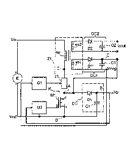
Figure 5 illustrates yet another example of a DC-DC converter object of
the invention. In this figure 5, the load is still a transformer with two
secondary
elements es1, es2. Each of them is connected to a rectifier circuit DC1, DC2.
In this
example, these rectifier circuits DC1, DC2 are similar to that referred to as
DC2 in
figure 4. The current unidirectional switch of the rectifier circuit DC1 is
referred to as D1'
and the electrical energy reservoir is referred to as Cr.
CA 02892330 2015-05-20
14
The common node between the current unidirectional switch D1' and
the electrical energy reservoir Cl' of the rectifier circuit DC1 is referred
to as E, it is
connected to the common node A between the normally ON switch element .11 and
the
normally OFF switch element M1 of the main switch K. The electrical energy
reservoir Cl' has one of its terminals connected to the node E and the other
connected
at the input of the control circuit G1 of the normally ON switch element J1.
This other
terminal is put to a potential Vneg which is negative with respect to the
potential
present at the common node A between the normally ON switch element .1i and
the
normally OFF switch element M1.
In this example, the main peak detector circuit DC is similar to that
illustrated in figures 1 and 3. The output of the main peak detector circuit
DC supplies
the control circuit G2 of the normally OFF switch element Ml. The voltage Vp
is positive
with respect to Vref.
Moreover, the normally ON switch element J1 is a current limiter
having an inhibition input driven by Vneg.
As described in figure 4, the rectifier circuit DC2 delivers an output DC
voltage Vout which is galvanically isolated from the voltage source E. This
voltage Vout
can supply an external circuit (not represented), for example a circuit for
controlling the
gate of a power transistor JFET.
The main advantage of the DC-DC voltage converter of the invention is
to have a linear operation for very low voltages of the voltage source and an
operation
through cutting for high voltages. This leads to a reduced power consumption
and thus
to a reduced thermal dissipation.
Another advantage of the DC-DC voltage converter is that it includes
fewer high voltage passive components than the starting circuit described in
the above
mentioned patent application.
Of course, some characteristics represented in these examples of
embodiments of the DC-DC voltage converter can be combined with each other
without
departing from the scope of the invention.