Note : Les descriptions sont présentées dans la langue officielle dans laquelle elles ont été soumises.
CA 02892775 2015-05-28
WO 2014/096771 PCT/GB2013/053142
1
LED DRIVER CIRCUIT USING FLYBACK CONVERTER TO REDUCE OBSERVABLE OPTICAL
FLICKER BY REDUCING
RECTIFIED AC MAINS RIPPLE
The present invention relates to a driver circuit for supplying
a drive current to an LED lighting scheme. In particular, the
present invention relates to an AC input driver circuit operable
in conjunction with a current regulator device as described in
United Kingdom Patent Application No. 1210561.5.
Whilst continued improvements in the cost and reliability of
Light Emitting Diodes (LEDs) have led to the wider adoption of
LED technology in the areas of indoor and outdoor lighting,
challenges exist in the provision of driver electronic circuitry
suitable for supplying a regulated current to LED lighting
systems. It is well known that variations in the drive current
supplied to an LED load can adversely affect performance. In
particular, LEDs which receive current from a power supply unit
(PSU) which takes a single-phase Alternating Current (AC) input
from a mains or similar supply, are sensitive to the presence of
residual "voltage ripple" resulting from incomplete suppression
of the AC component of the waveform emanating from a rectifier
circuit that sits at or near the input of the PSU, and which AC
component takes the form of a sinusoidal voltage at twice the
frequency of the AC voltage from the said mains or similar
supply.
LEDs, being diodes, exhibit in their operating region, low
differential impedance - defined as the rate of change of
voltage with current. This low differential impedance leads to
the generation of significant levels of ripple current in the
LEDs in the presence of voltage ripple. It can easily be shown
that, for small amounts of voltage ripple, the corresponding LED
current ripple can be expressed as:
Allot"A, Vde Vdc
õ., equation (1)
Vdc nod Z d
CA 02892775 2015-05-28
WO 2014/096771 PCT/GB2013/053142
2
Wherein, AVdc/Vdc is the peak-to-peak voltage ripple from the
PSU, expressed as a fraction of the operating DC voltage
provided by the PSU, Ailed/lied is the peak-to-peak LED current
ripple, expressed as a fraction of the operating LED current,
and Zd is the differential impedance of the LED chain at the
ripple frequency. The most important source of voltage ripple,
in the context of an LED lighting application, is the full-wave
rectification that occurs at the input to the PSU. This ripple
occurs at twice the mains AC frequency - so, between 100 and 120
Hz. Within this frequency range, research has shown that a high
proportion of healthy adults are sensitive to stroboscopic
effects arising from the presence of LED light flicker. Such
flicker is generated by the presence of current ripple within an
LED lighting fixture.
The sensitivity of LED current ripple to PSU voltage ripple can
easily be illustrated by reference to an example, relating to a
typical requirement for an LED-based street-lighting assembly,
in which an LED driver is used to provide a constant DC current
to a string of 40 series-connected white LEDs. Each LED has,
under normal operating temperatures, a voltage drop across it of
around 3.5V, leading to a total voltage across the LED string
(Vdc) of 140V. Furthermore, a typical white LED, operating at
3.5V, has a differential impedance of the order of 0.5 Ohm.
Therefore, in this illustrative example, Zd is around 20 Ohms.
Typical LED drive currents used in such an application are 350mA
or 700m.
If, in this illustrative example, the voltage ripple emanating
from the LED driver is as low as 1% of Vdc - a very low value,
typical of a very high quality LED driver - then, for 350mA
operation, the resulting LED current ripple would be around 20%
of lied, and for 700mA operation, it would be around 10% of
lied.
In view of the fact that in an LED, light output (luminous flux)
is directly related to current, this current ripple can in turn
lead to light flicker, which limits the acceptability of LED
CA 02892775 2015-05-28
WO 2014/096771 PCT/GB2013/053142
3
technology in applications such as office lighting, street
lighting and industrial lighting. Indeed, recent research has
shown sensitivity to stroboscopic effects arising from flicker
amongst healthy adults, even at very low flicker levels. In
fact, the research has indicated that at 10% flicker (resulting
from approximately 20% current ripple at 100Hz) around 75% of
healthy adults can detect stroboscopic effects arising from the
flicker. Such sensitivity to stroboscopic effects of flicker
represents a challenge to the widespread adoption of LED
lighting in applications where both comfort and accurate
perception of movement are important - particularly where the
scene being illuminated includes moving, oscillating, or
rotating objects.
There is therefore a need to reduce the voltage ripple emanating
from an AC input drive circuit used for supplying a drive
current an LED lighting scheme, in order to alleviate current
ripple and optical flicker.
This problem has been previously considered and attempts have
been made to provide LED driver circuits which seek to address
the problem of optical flicker arising as a consequence of the
periodic variation of an AC power supply. Specifically, the
provision of a capacitance at or near the output of the PSU
serves to smooth the voltage ripple arising from the PSU,
preferably down to levels of a few percent, as discussed above.
However, for various reasons relating to e.g. cost and
reliability, it is often advantageous for LED lighting schemes,
particularly those employed within street, office or industrial
lighting fixtures, to be constructed from long strings of series
connected LEDs, with each string being provided with a constant
DC current by a single driver. Thus, in order to ensure that
each driver produces sufficient light output from the string of
LEDs it is driving, it is necessary to ensure that its DC output
voltage is sufficiently high to drive a large number (typically,
several tens) of LEDs. In view of this, it is necessary for the
CA 02892775 2015-05-28
WO 2014/096771 PCT/GB2013/053142
4
electrical capacitors used for smoothing voltage ripple
emanating from the PSU to be capable of withstanding relatively
high DC voltages e.g. in the region of up to 200V or more. This
leads to the use of Electrolytic Capacitors, which in comparison
with other types of capacitor, are capable of withstanding such
voltages whilst providing high capacitance values, in the order
of hundreds of micro Farads . Furthermore, the need to reduce
voltage ripple to a minimum requires the use of high
capacitance. This can be achieved by using either a small number
of high value electrolytic capacitors, or a large number of
lower value electrolytic capacitors. The number of such
capacitors used to realize the required total capacitance is
determined at least in part, by the maximum rated ripple current
for each individual capacitor. However, the use of high value
Electrolytic capacitors or several low value electrolytic
capacitors increases the expected rate of capacitor failures
which, in turn, increases the statistical failure rate of the
PSU. The statistical failure rate of a PSU, or indeed any
electrical assembly, is normally expressed by use of its
reciprocal. This reciprocal (1/Statistical failure rate) is
referred to as the Mean Time Between Failures, or MTBF, of the
assembly.
It can therefore be appreciated that, in addition to minimizing
LED current ripple and flicker, as previously discussed, it is
also desirable to seek to reduce the number and capacitance of
Electrolytic Capacitors required at the output of the PSU
section of an LED driver with a view to improving the MTBF of
the LED driver. Preferably, the high MTBF performance should be
achieved without significantly compromising the current ripple
generated within a string of LEDs driven by the LED driver.
Indeed, it is desirable within the market, to ensure that the
peak-to-peak value of the current ripple within the LED chain
does not exceed around 196 of the DC current provided to the LED
chain, thereby significantly reducing and possibly eliminating
both directly and stroboscopically detectable flicker.
CA 02892775 2016-11-01
Thus, PSUs designed for use within LED drivers are often required -
particularly when aimed at the street, office and industrial lighting markets
- to address two opposing objectives. On the one hand, it is desirable for
the PSU to give low voltage ripple - thereby minimising LED current ripple
5 and optical flicker. On the other hand, it is desirable for the PSU to
exhibit
high reliability, corresponding to a low expected statistical failure rate.
The
first of these requirements often dictates the use of high capacitance at
the output of the PSU, which in turn dictates the use of either several
Electrolytic Capacitors, or high value Electrolytic Capacitors, or both.
Using high value Electrolytic Capacitors, or several low value ones
increases the expected rate of capacitor failures within a statistically
meaningful sample of such PSUs, thereby increasing the statistical failure
rate of the PSU.
In United Kingdom Patent Application No. 1210561.5, there is described a
current regulator for providing a regulated current from an input voltage.
The current regulator described in United Kingdom Patent Application No.
1210561.5 comprises a voltage regulation means comprising a plurality of
Zener diodes connected in parallel.
Application No. 1210561.5 describes a novel circuit topology whereby the
current through the regulator is, to within voltage limits defined by the
breakdown voltages of bipolar transistors, substantially constant with
applied DC voltage, as well as being substantially constant with
manufacturing variations in the properties of its component parts. It is
recognised by the present inventor that this high differential impedance
could be advantageously harnessed in order to mitigate the presence of
voltage ripple arising from an AC input PSU. Such a PSU should
advantageously be constructed in such a way that it can be integrated with
the regulator, whilst preferably allowing the regulator to operate at or near
its maximum efficiency.
CA 02892775 2015-05-28
WO 2014/096771 PCT/GB2013/053142
6
According to a first aspect of the present invention there is
provided a driver circuit for providing a regulated DC current
to a load from an AC supply, which load comprises an LED
lighting assembly, the driver circuit comprising: a rectifier
and a flyback converter, wherein the rectifier is operable in
use to convert an AC input voltage to a rectified voltage, which
rectified voltage is supplied to the flyback converter, and
wherein the flyback converter is operable in use to provide a
variable DC voltage to the load; a current regulator which forms
part of the load, the current regulator being series connected,
in use, to an LED lighting assembly; and feedback means operable
to maintain a constant DC voltage across the current regulator,
wherein the current regulator comprises voltage regulation means
comprising a plurality of Zener diodes connected in parallel.
Preferably the rectifier is a full-wave rectifier operable to
convert an AC input voltage to a full-wave rectified voltage
containing a DC voltage, which full-wave rectified voltage,
including its DC voltage component, is supplied to the flyback
converter.
Since embodiments of the present invention seek to minimise the
value of the output capacitance of the PSU, it is advantageous
to allow the PSU to produce an output voltage ripple, in the
order of a few Volts, peak-to-peak and to rely on the high
differential impedance of the regulator to provide the means by
which the current ripple in the LED string, arising as a result
of this PSU voltage ripple, is beneficially reduced. Thus,
embodiments of the present invention are advantageous in that
the PSU is preferably architected in such a way as to maintain a
substantially constant voltage across the current regulator so
that the high differential impedance of the current regulator
serves to quench the LED current ripple that would otherwise
arise from the voltage ripple.
A key feature of the current regulator described in United
Kingdom Patent Application No. 1210561.5 is that the Zener
CA 02892775 2015-05-28
WO 2014/096771 PCT/GB2013/053142
7
diodes exhibit the same nominal Zener voltage. A current
regulator constructed according to the teaching of United
Kingdom Patent Application No. 1210561.5 takes advantage of the
fact that, within a standard Zener diode fabrication process,
the standard variation in Zener voltages around the nominal
value is sufficiently small to allow current sharing between the
Zener diodes within the parallel combination. It can be defined
that a variation of between 0.1V and 0.3V may preferably exists
between the Zener voltages of the Zener diodes comprised in the
plurality of Zener diodes of the voltage regulation means.
According to a preferred embodiment of the present invention
each Zener diode has the same nominal Zener voltage. Whilst
having the same nominal Zener voltage, a variation of between
0.1V and 0.3V preferably exists between the Zener voltages of
the Zener diodes comprised in the plurality of Zener diodes of
the voltage regulation means.
A preferred embodiment of the current regulator taught in United
Kingdom Patent Application No. 1210561.5 is shown in Figure 1
and comprises a first current regulator circuit Cl cross-coupled
to a second current regulator circuit C2. The first current
regulator circuit Cl comprises a transistor circuit having a
resistor R1 and a bipolar transistor Tl. The first current
regulator circuit also comprises a voltage regulator circuit
VRC1 comprising a plurality of Zener diodes Z11, Z12... Z1n
connected in parallel. The second current regulator circuit C2
comprises a driver circuit having a resistor R2 and a bipolar
transistor T2. The second current regulator circuit also
comprises a voltage regulator circuit VRC2 comprising a
plurality of Zener diodes Z21, Z22... Z2n connected in parallel.
The transistor comprises a silicon bipolar transistor of the NPN
or PNP type. The transistors may form a complimentary pair -
e.g. the transistor of the first or second current regulator
circuit is of the PNP type whilst the transistor of other
current regulator circuit is of the NPN type. The resistor of
CA 02892775 2015-05-28
WO 2014/096771 PCT/GB2013/053142
8
the first and/or second transistor circuit is typically operable
to vary in order to serve as a current programming resistor.
The previously proposed current regulator operates from a DC
voltage rail and provides a substantially constant current,
suitable for driving an LED, or string of LEDs. Such a DC input
current regulator can beneficially provide a constant current
with a high setting accuracy and low thermal coefficient of
current. Advantageously, such a current regulator can be
programmed to provide a current over a range applicable to LED
lighting drivers. It is also possible for two such regulators to
be connected together in parallel, to provide higher currents,
e.g. in the order of 350mA to 700mA, whilst also providing a low
failure rate, of preferably less than 0.6 failures per million
hours. This advantageously corresponds to an MTBF for the
current regulator, in excess of 1.7 million hours.
According to a particularly preferred embodiment of the present
invention, the current regulator comprises a first current
regulator circuit and a second current regulator circuit,
wherein the output of the first current regulator circuit is
cross-coupled to said second current regulator circuit, each of
the first and second current regulator circuits comprising:
a transistor circuit comprising a resistor and a transistor; and
a voltage regulator circuit, forming said voltage regulation
means, the voltage regulator circuit operable to provide a
regulated voltage to the respective driver circuit, wherein said
voltage regulator circuit comprises a plurality of Zener diodes
connected in parallel.
Preferably, the operating voltage across the regulator is given
by:
Vreg an-Ft/rip/2 equation (2)
Wherein Vk is the knee voltage of the regulator and wherein Vrip
is the peak-to-peak ripple voltage provided by the PSU.
CA 02892775 2015-05-28
WO 2014/096771 PCT/GB2013/053142
9
Preferably, Vrip is no greater than Vk/2.
Preferably, therefore, the minimum DC voltage (Vreg(min))
provided in use to the current regulator is given by:
Vreg(Min)= 51,144
where Vk is the knee voltage of the current regulator.
Preferably, the current regulator comprises a two-terminal
circuit. Preferably, the Zener diodes of the/each voltage
regulator circuit comprise silicon Zener diodes. The Zener
diodes of the/each voltage regulator circuit may exhibit a Zener
voltage of less than 5.5V. Preferably the Zener diodes of
the/each voltage regulator circuit exhibit a Zener voltage of
between 2.0V and 3.0V.
Preferably, the Zener voltages of the Zener diodes comprised in
the voltage regulator circuit of the/each current regulator
circuit are selected such that:
Iz,opt = Tepee/2.N equation (3)
where Iz,opt is the current at which the rate of change of the
Zener voltage with temperature substantially equals the rate of
change of the base-emitter voltage vbe of the transistor of the
current regulator circuit, N is an integer number of Zener
diodes per voltage regulator circuit and 'spec is a current
regulator current at which the temperature coefficient is
substantially zero.
It will be appreciated that embodiments of the present invention
may be provided in conjunction with an LED lighting assembly,
typically comprising a string of LEDs connected in series, or
that the driver circuit may be provided separately for
connection to or integration with an LED lighting assembly.
CA 02892775 2015-05-28
WO 2014/096771 PCT/GB2013/053142
According to a second aspect of the present invention there is
provided an illumination apparatus comprising an LED lighting
assembly and a driver circuit according to the first aspect of
5 the present invention, wherein the LED lighting assembly is
connected in series with the current regulator to form part of
the load.
For a better understanding of the present invention, and to show
how the same may be carried into effect, reference will now be
10 made, by way of example, to the accompanying drawings in which:
Figure 1 shows a preferred embodiment of the current regulator
described in United Kingdom Patent Application No. 1210561.5;
Figure 2 shows a schematic an AC input LED driver according to
an embodiment of the present invention;
Figure 3 shows the current versus voltage characteristics of the
current regulator described in United Kingdom Patent Application
No. 1210561.5;
Figure 4 shows a schematic of a previously considered flyback
converter based power supply unit; and
Figure 5 shows a driver according to an embodiment of the
present invention comprising a flyback converter based power
supply unit.
Figure 2 shows a schematic an AC input LED driver according to
an embodiment of the present invention incorporating the current
regulator, connected to, or integrated with a PSU. The
capacitance, C,, placed at the output of the PSU provides a
means for reducing the voltage ripple from the PSU.
As discussed previously, in order to minimise the statistical
failure rate of the overall driver, this capacitance should be
minimised, and should be provided by a minimum number of
CA 02892775 2015-05-28
WO 2014/096771 PCT/GB2013/053142
11
electrolytic capacitors. It is a primary requirement within the
LED lighting and general illumination markets, that an AC input
LED driver should operate at a high level of efficiency -
defined as the ratio of output power, to input power, expressed
as a percentage. A preferred minimum level of efficiency for a
driver within these markets is around 85%, with a particularly
preferred level of 90%. The overall efficiency of a driver
according to the architecture shown in figure 2 is given by:
pe(D) = it(PSL)x it(Reg) equation (4)
Wherein, (PSU) is the efficiency of the PSU and (Reg) is the
efficiency of the regulator. The efficiency of the regulator,
when used in the manner shown in figure 2 is given by:
p(Reg) = (Vdc ¨ Vreg)fVdc equation (5)
Wherein, Vdc is the DC voltage provided by the PSU, and Vreg is
the voltage drop across the regulator. Therefore, (Reg) is
maximised by minimising Vreg as a fraction of Vdc. This places
two requirements on the PSU. Firstly, Vdc should preferably be
as high as possible, and secondly Vreg should be as low as
possible, whilst keeping the regulator operating in a manner
necessitated by the properties of the PSU.
Figure 3 shows the current versus voltage characteristic of the
current regulator disclosed in United Kingdom Patent Application
No. 1210561.5. Above a certain value of Vreg, the current drawn
by the regulator and, therefore, the current flowing through the
LED string is constant and is set to a value, Ic, which is
determined by the specific design of the regulator. This minimum
operating value of Vreg is known as the knee voltage (Vk) of the
regulator. Since preferred embodiments of the present invention
seek to minimise the value of Cc, the PSU may be allowed to
produce an appreciable voltage ripple, and to rely on the high
differential impedance of the regulator to provide the means by
CA 02892775 2015-05-28
WO 2014/096771 PCT/GB2013/053142
12
which the current ripple in the LED string, arising as a result
of this PSU voltage ripple, is reduced or minimised. For this to
occur, the operating voltage across the regulator, Vreg, should
preferably be:
Vreg Vk Vrip/2 equation (6)
Wherein, Vrip is the peak-to-peak ripple voltage provided by the
PSU. It is therefore preferable for the PSU to be operable so as
to maintain a substantially constant voltage across the
regulator, so that the high differential impedance of the
regulator is used to quench the LED current ripple that would
otherwise arise from the voltage ripple. This said constant
voltage should preferably be sufficiently higher than the
regulator's knee voltage to ensure that the ripple voltage is
subject to the said high differential impedance. At the same
time, however, in order to minimise Vreg, thereby maximising the
operating efficiency of the regulator, the value of Vrip should
not be allowed to exceed an appreciable fraction of Vk.
As a guide, Vrip is preferably no greater than Vk/2. This
ensures that the operating voltage of the regulator, Vreg, is
close to Vk, whilst accommodating an appreciable voltage ripple.
In this case, the minimum value of Vreg therefore becomes:
Vreg(frUit) = 517104 equation (7)
And the corresponding maximum value of overall efficiency of the
LED driver becomes:
svk
pi(D, Max) = 105'0x equation (8)
4Vex
The knee voltage, Vk, for a current regulator based on the
architecture disclosed in reference 1 is around 6V.
The power delivered to the LED chain is given by:
CA 02892775 2015-05-28
WO 2014/096771
PCT/GB2013/053142
13
P(LED) = fled z (Vdc --wk) equation ( 9 )
4
Therefore, by way of example, assuming an LED current of 700mA
(achievable using a regulator comprising two of the regulators
disclosed in United Kingdom Patent Application No.
1210561.5reference 1, connected in parallel) achieving an output
power, delivered to the LED chain, of 120 Watts requires a DC
rail voltage from the PSU, of 179V. Furthermore, for this
particular example, achieving an overall efficiency of 85% or
greater, for the LED driver would require the PSU to have an
efficiency of 89% or greater.
For the driver architecture shown in figure 2, the differential
impedance, Zd, that impedes ripple current in the LED chain is
that of the current regulator.
A 350mA current regulator, employing the topology disclosed in
United Kingdom Patent Application No. 1210561.5, is capable of
delivering a differential impedance (dV/dI) greater than 2 KS-2 at
frequencies up to around 200 Hz. Therefore, such a current
regulator, when integrated with an ac input dc output PSU that
provides the ability to maintain a substantially constant DC
voltage across the regulator, together with a maximum DC rail
voltage of at least 179 V, with a peak-to-peak voltage ripple of
3V, would provide an LED driver capable of delivering a constant
current of 350mA, to an LED string, with a peak-to-peak LED
current ripple as low as 0.4%. A 700mA version of the same LED
driver, realised by changing the current programming resistors
in the current regulator, would deliver an LED drive current of
700mA, with a peak-to-peak LED current ripple as low as 0.2%.
A further advantageous property of the DC current regulator
disclosed in United Kingdom Patent Application No. 1210561.5 is
its high MTBF, afforded by the absence of capacitors, the small
number of transistors (4 for a 350mA or 700mA regulator,
CA 02892775 2015-05-28
WO 2014/096771 PCT/GB2013/053142
14
comprising two of the circuits disclosed in the reference) and
the fact that these transistors are of a bipolar type. In order
to take fullest advantage of this property when integrated into
an LED driver, it is beneficial to combine a regulator according
to this architecture, with a PSU that, as well as possessing the
properties outlined above, also has a high MTBF. Achieving this
is partly enabled by using only a small number of Electrolytic
Capacitors at the output of the PSU, as facilitated by the high
differential impedance of the regulator. It would be further
enabled, for a generalised switch-mode power supply, by the use
of a high maximum DC output voltage, which is known in the art
to result in high efficiency operation for switch-mode
circuitry. Such high efficiency leads to low power dissipation
within the PSU, for a given output power, thereby contributing
to a high MTBF for the same given output power.
A third contributing factor to achieving high PSU MTBF for a
given power level and efficiency, is the minimisation of the
component count within the PSU. It is known that for medium
power levels (100s of Watts) a generalised switch-mode PSU that
achieves these power levels with a low component count is one
based on a Flyback Converter.
Figure 4 shows the schematic of a previously considered Flyback
Converter based PSU, configured to accommodate a range of load
voltages. As will be appreciated by those skilled in the art the
circuit operates by successively charging and discharging the
primary inductive coil of a transformer, T, through the
switching action of a Mosfet, S, which is controlled by a
controller, C, through the application by C, of a rectangular
voltage waveform, with a duty cycle, D, defined as the
proportion of time that the said waveform spends in its ON-
state, during which time the voltage provided by C is at a
positive value, sufficient to turn the Mosfet on. The PSU
provides a means of transferring electrical power from a time
varying input voltage, Vin, provided by a bridge rectifier, B,
connected to a smoothing capacitor, Cs, to a time varying output
CA 02892775 2015-05-28
WO 2014/096771 PCT/GB2013/053142
voltage, Vout. The voltage transfer ratio of the PSU (Vout/Vin)
is determined mainly by the duty cycle, D, of the switching
Mosfet and the turns-ratio, N, of the transformer, where N is
here the ratio between the number of turns in the secondary coil
5 of the transformer, to the number of turns in the primary coil
of the transformer, according to the following relationship:
Vout=111-nxMcDif(1¨D) equation (10)
10 It will be appreciated by a reader skilled in the art, that
power supplies using a flyback converter topology are normally
operated in such a manner that the duty cycle, D, of the
switching Mosfet is varied, typically together with the
frequency of switching, across the time period of each half
15 cycle of the rectified output of the rectifier, in order to
ensure that the current drawn from the rectifier is
substantially in phase with the voltage supplied by the
rectifier. The value of D in equation 10 varies, together with
the frequency of the switching action of the Mosfet, S, as Vin
varies, across each half cycle of its time domain waveform. In
cases where the DC component of Vout is low (10s of Volts) the
voltage drop across the output diode shown as Do in figure 3,
being around 1V during the period of the switching waveform
during which it is conducting, becomes an appreciable fraction
of the output voltage, thereby requiring this voltage drop to be
taken into account. However, for a Flyback Converter with an
output voltage of several lOs of volts or more, the effect of
this voltage drop is neglected.
It is clear from equation 9 that, in order to accommodate a
varying output voltage arising as a result of a varying load,
the duty cycle, D, for any instantaneous value of Vin, needs to
change in response to variations in the load. Such variations
would occur, in the case of a load comprising, at least in part,
a series string of LEDs, due to either changes in temperature,
or changes in the number of LEDs in the string, or both.
Altering the duty cycle of the switching Mosfet is actuated by
CA 02892775 2015-05-28
WO 2014/096771 PCT/GB2013/053142
16
feeding a voltage back to the Controller, via a feedback
element, F, which normally takes the form of an Opto-isolator.
The Controller is configured in such a way that, in response to
the input from F, it alters the duty cycle, D, of a Pulse Width
Modulated voltage applied to the gate of the Mosfet, thereby
switching the Mosfet on and off with the same duty cycle as the
Pulse Width Modulated voltage.
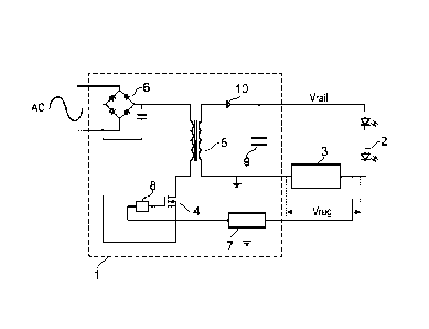
Figure 5 shows an LED driver comprising a an AC input, DC output
power supply unit wherein the output DC voltage is controlled by
a flyback converter and wherein the PSU is connected to, or
integrated with a low-side constant current regulator, where the
said regulator is based on a current regulator as disclosed in
United Kingdom Patent Application No. 1210561.5.
When used in combination with the current regulator, 3, the PSU,
1, needs to provide a DC rail voltage (Vrail) at the top of the
LED string, 2, which varies in response to the size of the load,
as determined by the number of LEDs in the string, and
temperature, whilst maintaining a constant voltage, Vreg, across
the current regulator, 3. Due to the current regulating action
of the regulator, 3, together with the fact that it is connected
in series with the LED string, 2, by using the feedback control
mechanism to control the voltage drop, Vreg, across the
regulator, the rail voltage, Vrail takes a value given by the
sum of the voltage drop across the LED string, 2, and Vreg. If
the voltage drop across the LED string is denoted as Vied, then
Vrail = Vled + Vreg. Furthermore, the value of Vrail is
determined by the duty cycle of the switching Mosfet, 4, the
turns ratio, N, of the transformer, 5, and the DC component of
the rectified mains input voltage supplied to the Flyback
Converter, by the input mains rectifier, 6, as discussed
previously. Therefore:
Vrail = Vtn x x ¨ equation (11)
And Vreg is given by:
CA 02892775 2015-05-28
WO 2014/096771 PCT/GB2013/053142
17
Vreg = Vin x N x¨D ¨Vied equation (12)
-D
Therefore, if, as in figure 5, the feedback mechanism provided
by the Opto-isolator, 7, is used as shown, to adjust the duty
cycle, D, of the output of the Controller, 8, to maintain a
constant value of Vreg, then the feedback mechanism becomes a
means for accommodating a varying value of Vled. The range of
values of Vled that can be accommodated by a single LED driver
according to the topology of figure 5 is determined, for a given
value of turns ratio, N, by a number of factors, including the
range of duty cycles that can be provided by the Controller, 9,
the thermal handling properties of the switching Mosfet, 4, and
the maximum withstand voltage of the output capacitor, 9, which
is charged via diode 10, during each OFF portion of the
switching waveform applied to the gate of the switching Mosfet,
4.
The value of the output capacitor, 9, which may be realised by
either a single capacitor, or by a parallel combination of
capacitors, is chosen by reference to the required output
voltage ripple from the PSU. This voltage ripple can, in
accordance with earlier argumentation, be as high as 3V, when
running a regulator of the type disclosed in United Kingdom
Patent Application No. 1210561.5, near its peak DC efficiency.
The value of the output capacitor, 9, required to give a peak-
to-peak output voltage ripple of Vrip, can be expressed, to a
good approximation, as:
Co ¨ _______________ equation (13)
.4a(PSL1).Vrip
Wherein, co is the mains angular frequency, and is therefore
equal to 2xExf, where f = 50 Hz in the UK. Therefore, if the
efficiency of the PSU is equal to the minimum acceptable value
of 89% ( (D) = 0.89) and Vrip is 3V, the minimum capacitance
CA 02892775 2015-05-28
WO 2014/096771 PCT/GB2013/053142
18
provided by the output capacitor, 11, is 835 F for 700mA
operation. However this capacitance, or one slightly greater, is
realised, each individual capacitor is required to have a rated
voltage that is significantly greater than the maximum value of
Vrail. Therefore, for operation at output voltages up to 179V,
each capacitor should be rated to at least 300V.
The number of parallel capacitors used to realise Co is
determined by ensuring that the ripple current in each capacitor
does not exceed the maximum ripple current for an available,
affordable, high quality Electrolytic Capacitor with a voltage
rating of 300V or greater. A typical, affordable realisation of
Co is a parallel connected pair of 440 F, 300V Aluminium
Electrolytic Capacitors, giving a total output capacitance of
880 F.
The value of Vled is a function of the number of LEDs in the
string, N, the current flowing in the LED string, lied, and the
LED junction temperature, Tj. In any particular embodiment of
the circuit according to the topology shown in figure 5, the LED
current, lied, is determined by the current setting
functionality of the regulator, 3, provided by the appropriate
selection of current setting resistor values, as described in
United Kingdom Patent Application No. 1210561.5. Therefore, in
any particular embodiment of the circuit in figure 5, the value
of Vied is a function of N and Tj. Consequently, embodiments of
the present invention advantageously provide a means by which
the current regulator disclosed in United Kingdom Patent
Application No. 1210561.5 can be integrated into an AC input LED
driver to accommodate a varying LED load, over a range defined
by the voltage and thermal properties of the main electrical
components. Thus, embodiments of the present invention
advantageously provide for the realisation of LED drivers,
leveraging the ripple current suppression, current setting
accuracy and thermal tracking properties of the current
regulator disclosed in United Kingdom Patent Application No.
CA 02892775 2015-05-28
WO 2014/096771 PCT/GB2013/053142
19
1210561.5, whilst beneficially operating the said current
regulator at or near its maximum efficiency.
Illustrative example:
The following example of an embodiment of the invention is
presented for purposes of illustration and it should be apparent
to the reader that numerous other embodiments and illustrative
examples, bounded by output voltage from the PSU section, the
current drawn by the LED string and the mains voltage and
frequency, are achievable.
This, or any other example of the present invention, is
explained in terms of the relevant design parameters of the PSU
section and current regulator section of the LED driver.
The peak output voltage of the PSU section of the driver is
given by:
V op = Vim" x N x Dp1(1¨ Dp) equation (14)
Wherein, Dp is the peak duty cycle of the switching action of
the switching Mosfet, and Vinp is the peak value of a full-wave
rectified single-phase mains voltage, whichis given by:
rap = Vrirts x 11-2. ¨ 2nrci equation (15)
Wherein, Vrms is the root-mean-square mains voltage and vd is
the voltage drop across a single diode within the rectifier,
during the half cycle of the mains input during which the said
diode is conducting current. The typical value of vd for a
Silicon rectifying diode is around 0.8V.
Vop in equation 14 is related to the DC component, Vo, of the
output voltage, by the following equation:
CA 02892775 2015-05-28
WO 2014/096771 PCT/GB2013/053142
Vop = limn/2 equation (16)
Therefore, the values of Dp (peak Mosfet switching Duty Cycle)
that corresponds to the maximum PSU output voltage, Vo,max given
5 by:
El; Max = r/(2 \ !":-Ynsxµri ¨ 4Nrel \1AX)
equation (17)
An illustrative example of the PSU section of an LED driver,
according to embodiments of the present invention can be
defined, in terms of its range its maximum Mosfet duty cycle ,
when employing a transformer with a turns ratio of 2 and when
operating from an RMS mains voltage of 230V, and being required
to give a maximum output voltage of 180V.
Dp, Max = 0.304 = 30.4% equation (18)
The corresponding maximum peak-to-peak ripple current in the
output capacitor is given, by standard flyback converter design
equations, as:
ic, pp = limas x Dp,Max X 101-2 ALpXNXISIV) equation (19)
Wherein, Lp is the inductance of the primary of the transformer
and fsw is the nominal frequency of the switching waveform
applied to the Mosfet, by the controller. Using typical values
of 0.75 mH and 200 KHz, for this example, the peak-to-peak
capacitor ripple current is equal to 326mA.
As previously discussed, in order to produce a peak-to-peak
output voltage ripple of 3V at maximum output voltage, when
connected to a 700mA current regulator the output capacitance
needs to be at least 835 F. Given the need to minimise the
CA 02892775 2015-05-28
WO 2014/096771 PCT/GB2013/053142
21
current ripple through any single capacitor, whilst keeping the
number of capacitors to a minimum, as well as operating well
below the rated voltage of the capacitors used, an output
capacitance around 5 percent greater than this minimum is best
realised by two 440 'IF, 300V electrolytic capacitors, connected
in parallel.
The current regulator, connected to the PSU, as shown in figure
5, may be configured to provide a constant current of 700mA for
the purposes of the present example. Using the disclosure of
United Kingdom Patent Application No. 1210561.5, this particular
regulator would be realised by using two regulator circuits,
connected in parallel, where each such regulator circuit takes
the form shown in Figure 1 and where, by reference to the said
Fig 6, for the single regulator:
IT= 350m4 equation
(20)
By using the relevant design equation given in United Kingdom
Patent Application No. 1210561.5, and putting R1 = R2 = R:
vz-:the
R = 2x equation (21)
IT
Yielding, in accordance with the values given in United Kingdom
Patent Application No. 1210561.5 (vbe 0.7V and Vz = 3 V) R
13 Q.
The other design variable for a regulator of the type disclosed
in United Kingdom Patent Application No. 1210561.5 is the number
of Zener diodes, each with a Zener voltage of 2.4 V at a
reference current of 5 mA, used in each of the regulators. In
United Kingdom Patent Application No. 1210561.5, this is
determined, for a given value of regulator current, by assuming
that the thermal coefficient of regulated current needs to be
substantially zero. Following the procedure outlined in United
Kingdom Patent Application No. 1210561.5, wherein the current
CA 02892775 2015-05-28
WO 2014/096771 PCT/GB2013/053142
22
through each diode is preferable required to be around 14.5mA,
realising a single current regulator with a regulated current of
350mA and with a thermal coefficient of current that is
substantially zero, would require 12 Zener diodes in each 'Zener
stack' as defined in United Kingdom Patent Application No.
1210561.5. However, for the general case of a current regulator
according to the invention of United Kingdom Patent Application
No. 1210561.5, the thermal coefficient of the regulated current
is given by equation 18 of United Kingdom Patent Application No.
1210561.5, as:
ET2 E'vfze
TC = _____________________________________________ equation (22)
vss-vbe
Where the thermal coefficient of the base-emitter voltage of a
Silicon bipolar transistor, 6vbe/oT is, to a good approximation,
-2.0mV/K. From inspection of the thermal characteristic of a
typical 2.4V Silicon Zener diode (where 2.4V is the value of Vz
at a reference current of 5mA) the value of 6V.z/8T at twice the
optimal Zener current (2 x 14.5 mA = 29 mA) is around -2.2 mV/K.
The value of Vz at this current, for the same typical Silicon
diode is 3V. Therefore, the temperature coefficient of current
for the 350mA current regulator, used in this illustrative
example is -87ppm/K. This shows that the number of Zener diodes
per 'Zener stack' in each of the two 350mA current regulators
used within this illustrative example can be reduced from 12 to
6, whilst maintaining a low temperature coefficient of current.
Thus, the illustrative example, defined above, is achievable,
using a PSU according to the modified flyback converter topology
shown in figure 5, in which the current regulator (3) takes the
form of two parallel connected current regulator circuits, as
disclosed in United Kingdom Patent Application No. 1210561.5,
and wherein: For the PSU, driven from a 230V, 50Hz mains supply:
Vout = 60 to 180V, D,Max = 30,5, N =2, Co takes the form of two
CA 02892775 2015-05-28
WO 2014/096771
PCT/GB2013/053142
23
440 F, 300V rated electrolytic capacitors, fsw . 200 KHz, and
the primary inductance of the transformer is 0.75 mH.
For each of the two current regulator circuits contained within
the current regulator (3): Each Zener stack, as shown in Fig 1
comprises 6 Silicon Zener diodes, each with a Zener voltage of
2.4 V at a reference current of 5mA, and each resistor, shown as
R1 and R2 in Fig 1 takes the value 13f1