Note : Les descriptions sont présentées dans la langue officielle dans laquelle elles ont été soumises.
CA 02896486 2015-06-25
WO 2014/130026 PCT/US2013/026894
OPTICAL DESIGN TECHNIQUES FOR PROVIDING
FAVORABLE FABRICATION CHARACTERISTICS
BACKGROUND
[0001] The present invention relates to optical computing devices and,
more particularly, to optical design techniques that provide favorable
fabrication
characteristics for optical elements used in optical computing devices.
[0002] Optical computing devices, also commonly referred to as
"opticoanalytical devices," can be used to analyze and monitor a substance in
real time. Such optical computing devices will often employ a processing
element that optically interacts with the substance to determine quantitative
and/or qualitative values of one or more physical or chemical properties of
the
substance. The processing element may be, for example, an integrated
computational element (ICE), also known as a multivariate optical element
(MOE), which is essentially an optical interference filter that can be
designed to
operate over a continuum of wavelengths in the electromagnetic spectrum from
the UV to mid-infrared (MIR) ranges, or any sub-set of that region.
Electromagnetic radiation that optically interacts with the ICE is changed so
as to
be readable by a detector, such that an output of the detector can be
correlated
to the physical or chemical property of the substance being analyzed.
[0003] One exemplary type of ICE includes a plurality of layers
consisting of various materials whose index of refraction and size (e.g.,
thickness) may vary between each layer. An ICE design refers to the number
and thickness of the respective layers of the ICE component. The layers may be
strategically deposited and sized so as to selectively pass predetermined
fractions of electromagnetic radiation at different wavelengths configured to
substantially mimic a regression vector corresponding to a particular physical
or
chemical property of interest.
Accordingly, an ICE design will exhibit a
transmission function that is weighted with respect to wavelength. After the
electromagnetic radiation from a light source interacts with a sample and ICE,
the output light is conveyed to an optical transducer or detector. The total
intensity measured by the detector is related to the physical or chemical
property of interest for the substance.
[0004] It has been found, however, that the resulting transmission
function for some ICE designs may change or shift based on errors in
fabricating
1
CA 02896486 2015-06-25
WO 2014/130026 PCT/US2013/026894
the individual ICE components. For example, during fabrication of an ICE
component, slight errors may be made while depositing one or more of its
layers. While some errors in a particular layer might cause a large shift in
the
transmission spectra of the ICE component as a whole, such errors may not be
detrimental to the prediction performance of the ICE component. On the other
hand, errors on another layer may cause only a slight spectral shift in the
transmission profile, but this small shift may be significant with respect to
prediction performance. It may be advantageous to determine which ICE
designs may have hypersensitive layers for which extra care should be taken
during the fabrication process to ensure minimal layer error.
SUMMARY OF THE INVENTION
[0005] The present invention relates to optical computing devices and,
more particularly, to optical design techniques that provide favorable
fabrication
characteristics for optical elements used in optical computing devices.
[0006] In some embodiments, a method of evaluating an optical
element for fabrication is disclosed. The method may include randomizing a
design thickness of each layer of a desired integrated computational element
(ICE) design to simulate a fabrication error in each layer, thereby generating
a
plurality of randomized ICE designs, calculating a standard error of
calibration
for each randomized ICE design, correlating the standard error of calibration
between a given layer of the desired ICE design and the fabrication error of
each
corresponding layer of each randomized ICE design, and ranking the plurality
of
layers of the desired ICE design based on the sensitivity to changes in the
standard error of calibration.
[0007] In other embodiments, a method of evaluating and fabricating
an optical element is disclosed. The method may include altering a design
thickness of each layer of a desired integrated computational element (ICE)
design to simulate a fabrication error in each layer, thereby generating a
plurality of randomized ICE designs, calculating a standard error of
calibration
between each randomized ICE design and the desired ICE design, correlating the
standard error of calibration between a given layer of the desired ICE design
and
the fabrication error of each corresponding layer of each randomized ICE
design,
ranking the plurality of layers of the desired ICE design based on the
sensitivity
to changes in the standard error of calibration, and depositing each sensitive
layer with increased accuracy and precision.
2
CA 02896486 2015-06-25
WO 2014/130026 PCT/US2013/026894
[0008] The features and advantages of the present disclosure will be
readily apparent to those skilled in the art upon a reading of the description
of
the preferred embodiments that follows.
BRIEF DESCRIPTION OF THE DRAWINGS
[0009] The following figures are included to illustrate certain aspects of
the present invention, and should not be viewed as exclusive embodiments. The
subject matter disclosed is capable of considerable modifications,
alterations,
combinations, and equivalents in form and function, as will occur to those
skilled
in the art and having the benefit of this disclosure.
[0010] FIG. 1 illustrates an exemplary integrated computation element,
according to one or more embodiments.
[0011] FIG. 2 illustrates a schematic flowchart of a method of
evaluating an ICE design for fabrication, according to one or more
embodiments.
[0012] FIG. 3 illustrates a plot that depicts a transmission spectrum for
an exemplary randomized ICE design.
[0013] FIG. 4 illustrates a sensitivity plot depicting the sensitivity of
each layer of the randomized ICE design of FIG. 3.
[0014] FIG. 5 illustrates a fabrication sensitivity plot corresponding to a
desired ICE design.
DETAILED DESCRIPTION
[0015] The present invention relates to optical computing devices and,
more particularly, to optical design techniques that provide favorable
fabrication
characteristics for optical elements used in optical computing devices.
[0016] The present disclosure facilitates the evaluation of desired
integrated computational element (ICE) designs to determine how layer errors
due to physical fabrication methods affect chemometric predictability. Instead
of
calculating the mean squared error (MSE) from the spectral changes of the ICE
design, the present disclosure uses the standard error of calibration (SEC).
As a
result, the methods disclosed herein may be able to determine which layers of
a
desired ICE design would be more sensitive to fabrication errors and would
therefore detrimentally impact the overall SEC of a batch of the desired ICE
design. Once an operator knows which layers are more sensitive to fabrication
errors than others, additional care and precision may be taken in physically
depositing those sensitive layers.
3
CA 02896486 2015-06-25
WO 2014/130026 PCT/US2013/026894
[0017] The methods disclosed herein may help an operator determine if
a particular desired ICE design contains hypersensitive layers in which small
deposition layer errors may be capable of degrading chemometric predictability
to a point where the desired ICE design would be rendered useless or otherwise
ineffective for its intended purpose. Moreover, using the methods disclosed
herein, an operator may be able to intelligently determine which batch of a
desired ICE design would be more desirable than another due to a lower average
batch SEC. Therefore, the methods disclosed herein may also help an operator
determine which desired ICE design is more preferred over other desired ICE
designs.
[0018] The disclosed systems and methods may be suitable for
designing, evaluating, and fabricating ICE components for use in the oil and
gas
industry which oftentimes deploys optical computing devices in environments
exhibiting extreme conditions. It will be appreciated, however, that the
various
disclosed systems and methods are equally applicable to designing and
fabricating ICE components for use in other technology fields including, but
not
limited to, the food and drug industry, industrial applications, mining
industries,
or any field where it may be advantageous to determine in real-time or near
real-time a characteristic of a specific substance, but where the
environmental
factors, such as temperature, pressure, and humidity, have a critical impact
in
monitoring applications.
[0019] As used herein, the term "characteristic" refers to a chemical,
mechanical, or physical property of a substance. A characteristic of a
substance
may include a quantitative or qualitative value of one or more chemical
constituents or compounds present therein or any physical property associated
therewith. Such chemical constituents and compounds may be referred to
herein as "analytes." Illustrative characteristics of a substance that can be
monitored with the optical computing devices described herein can include, for
example, chemical composition (e.g., identity and concentration in total or of
individual components), phase presence (e.g., gas, oil, water, etc.), impurity
content, pH, alkalinity, viscosity, density, ionic strength, total dissolved
solids,
salt content (e.g., salinity), porosity, opacity, bacteria content, total
hardness,
combinations thereof, state of matter (solid, liquid, gas, emulsion, mixtures,
etc), and the like.
4
CA 02896486 2015-06-25
WO 2014/130026 PCT/US2013/026894
[0020] As used herein, the term "electromagnetic radiation" refers to
radio waves, microwave radiation, infrared and near-infrared radiation,
visible
light, ultraviolet light, X-ray radiation and gamma ray radiation.
[0021] As used herein, the term "optical computing device" refers to an
optical device that is configured to receive an input of electromagnetic
radiation
associated with a substance and produce an output of electromagnetic radiation
from a processing element arranged within the optical computing device. The
processing element may be, for example, an integrated computational element
(ICE), also known as a multivariate optical element (MOE). The electromagnetic
radiation that optically interacts with the processing element is changed so
as to
be readable by a detector, such that an output of the detector can be
correlated
to a particular characteristic of the substance. The output of electromagnetic
radiation from the processing element can be reflected, transmitted, and/or
dispersed electromagnetic radiation. Whether the detector analyzes reflected,
transmitted, or dispersed electromagnetic radiation may be dictated by the
structural parameters of the optical computing device as well as other
considerations known to those skilled in the art. In addition, emission and/or
scattering of the fluid, for example via fluorescence, luminescence, Raman,
Mie,
and/or Raleigh scattering, can also be monitored by optical computing devices.
[0022] As used herein, the term "optically interact" or variations thereof
refers to the reflection, transmission, scattering, diffraction, or absorption
of
electromagnetic radiation either on, through, or from one or more processing
elements (i.e., ICE or MOE components) or a substance being analyzed by the
processing elements.
Accordingly, optically interacted light refers to
electromagnetic radiation that has been reflected, transmitted, scattered,
diffracted, or absorbed by, emitted, or re-radiated, for example, using a
processing element, but may also apply to interaction with a substance.
[0023] As mentioned above, the processing element used in the above-
defined optical computing devices may be an integrated computational element
(ICE). In operation, an ICE is capable of distinguishing electromagnetic
radiation related to a characteristic of interest of a substance from
electromagnetic radiation related to other components of the substance.
Referring to FIG. 1, illustrated is an exemplary ICE 100, according to one or
more embodiments. As illustrated, the ICE 100 may include a plurality of
alternating layers 102 and 104, such as silicon (Si) and Si02 (quartz),
5
CA 02896486 2015-06-25
WO 2014/130026 PCT/US2013/026894
respectively. In general, these layers 102, 104 consist of materials whose
index
of refraction is high and low, respectively. Other examples of materials might
include niobia and niobium, germanium and germania, MgF, SiO, and other high
and low index materials known in the art. The layers 102, 104 may be
strategically deposited on an optical substrate 106. In some embodiments, the
optical substrate 106 is BK-7 optical glass. In other embodiments, the optical
substrate 106 may be another type of optical substrate, such as quartz,
sapphire, silicon, germanium, zinc selenide, zinc sulfide, or various plastics
such
as polycarbonate, polymethylmethacrylate (PMMA), polyvinylchloride (PVC),
diamond, ceramics, combinations thereof, and the like.
[0024] At the opposite end (e.g., opposite the optical substrate 106 in
FIG. 1), the ICE 100 may include a layer 108 that is generally exposed to the
environment of the device or installation, and may be able to detect a sample
substance. The number of layers 102, 104 and the thickness of each layer 102,
104 are determined from the spectral attributes acquired from a spectroscopic
analysis of a characteristic of the substance being analyzed using a
conventional
spectroscopic instrument. The spectrum of interest of a given characteristic
typically includes any number of different wavelengths. It should be
understood
that the exemplary ICE 100 in FIG. 1 does not in fact represent any particular
characteristic of a given substance, but is provided for purposes of
illustration
only.
Consequently, the number of layers 102, 104 and their relative
thicknesses, as shown in FIG. 1, bear no correlation to any particular
characteristic.
Nor are the layers 102, 104 and their relative thicknesses
necessarily drawn to scale, and therefore should not be considered limiting of
the present disclosure. Moreover, those skilled in the art will readily
recognize
that the materials that make up each layer 102, 104 (i.e., Si and 5i02) may
vary, depending on the application, cost of materials, and/or applicability of
the
material to the given substance being analyzed.
[0025] In some embodiments, the material of each layer 102, 104 can
be doped or two or more materials can be combined in a manner to achieve the
desired optical characteristic. In addition to solids, the exemplary ICE 100
may
also contain liquids and/or gases, optionally in combination with solids, in
order
to produce a desired optical characteristic. In the case of gases and liquids,
the
ICE 100 can contain a corresponding vessel (not shown), which houses the
gases or liquids. Exemplary variations of the ICE 100 may also include
6
CA 02896486 2015-06-25
WO 2014/130026 PCT/US2013/026894
holographic optical elements, gratings, piezoelectric, light pipe, and/or
acousto-
optic elements, for example, that can create transmission, reflection, and/or
absorptive properties of interest.
[0026] The multiple layers 102, 104 exhibit different refractive indices.
By properly selecting the materials of the layers 102, 104 and their relative
thickness and spacing, the ICE 100 may be configured to selectively
pass/reflect/refract predetermined fractions of electromagnetic radiation at
different wavelengths. Each wavelength is given a predetermined weighting or
loading factor. The thickness and spacing of the layers 102, 104 may be
determined using a variety of approximation methods from the spectrum of the
characteristic or analyte of interest. These methods may include inverse
Fourier
transform (IFT) of the optical transmission spectrum and structuring the ICE
100
as the physical representation of the IFT. The approximations convert the IFT
into a structure based on known materials with constant refractive indices.
Further information regarding the structures and design of exemplary ICE
elements is provided in Applied Optics, Vol. 35, pp. 5484-5492 (1996) and Vol.
29, pp. 2876-2893 (1990), which are hereby incorporated by reference.
[0027] The weightings that the layers 102, 104 of the ICE 100 apply at
each wavelength are set to the regression weightings described with respect to
a
known equation, or data, or spectral signature. When electromagnetic radiation
interacts with a substance, unique physical and chemical information about the
substance may be encoded in the electromagnetic radiation that is reflected
from, transmitted through, or radiated from the substance. This information is
often referred to as the spectral "fingerprint" of the substance. The ICE 100
may be configured to perform the dot product of the electromagnetic radiation
received by the ICE 100 and the wavelength dependent transmission function of
the ICE 100. The wavelength dependent transmission function of the ICE 100 is
dependent on the layer material refractive index, the number of layers 102,
104
and the layer thicknesses. The ICE 100 transmission function is then analogous
to a desired regression vector derived from the solution to a linear
multivariate
problem targeting a specific component of the sample being analyzed. As a
result, the output light intensity of the ICE 100 is related to the
characteristic or
analyte of interest.
[0028] The optical computing devices employing such an ICE 100 may
be capable of extracting the information of the spectral fingerprint of
multiple
7
CA 02896486 2015-06-25
WO 2014/130026 PCT/US2013/026894
characteristics or analytes within a substance and converting that information
into a detectable output regarding the overall properties of the substance.
That
is, through suitable configurations of the optical computing devices,
electromagnetic radiation associated with characteristics or analytes of
interest
in a substance can be separated from electromagnetic radiation associated with
all other components of the substance in order to estimate the properties of
the
substance in real-time or near real-time. Further details regarding how the
exemplary ICE 100 is able to distinguish and process electromagnetic radiation
related to the characteristic or analyte of interest are described in U.S.
Patent
Nos. 6,198,531; 6,529,276; and 7,920,258, incorporated herein by reference in
their entirety.
[0029] Before an ICE component is physically fabricated for use one or
more theoretical designs of the ICE component are typically generated. Such
theoretical designs may be generated using, for example, a computer-based
software program or design suite that may be stored on a computer-readable
medium containing program instructions configured to be executed by one or
more processors of a computer system. The design suite may be configured to
generate several theoretical ICE designs, each being configured or otherwise
adapted to detect a particular characteristic or analyte of interest.
[0030] In some embodiments, the design suite may commence the
design process by generating a single theoretical ICE design that has a random
number of layers and/or a random layer thickness for each layer. The design
suite may then proceed to optimize the number of layers and/or layer
thicknesses of the ICE design based on several "figures of merit" or
performance
criteria. Such performance criteria may include, but are not limited to,
minimum
prediction error, standard error of calibration (SEC), standard error of
performance (SEP), sensitivity, slope of the calibration curve, signal-to-
noise
ratio, and mean transmission value corresponding to the particular
characteristic
or analyte of interest. During this optimization process, the design suite may
be
configured to vary layer thicknesses and/or remove layers until several
designs
of the ICE component are generated that meet one or more minimum criteria for
predicting the analyte of interest. Several thousands of varying ICE designs
may
be generated from the theoretical ICE component during this stage.
[0031] Once these theoretical ICE component designs are generated,
they may be sorted by the design suite based on, for example, prediction error
8
CA 02896486 2015-06-25
WO 2014/130026 PCT/US2013/026894
and signal. In some cases, the various ICE designs may be sorted based on
their overall SEC (i.e., chemometric predictability) as tested against a known
value for the characteristic or analyte of interest. For example, the SEC for
each
ICE design may be calculated by taking the square root of the sum of squares
between the known value for the analyte of interest and the predicted value as
derived from the transmission spectrum of the particular ICE design. This is
accomplished for each theoretical ICE design by calculating its respective
transmission spectrum and applying that transmission spectrum to the known
data set of the analyte of interest.
[0032] In some embodiments, the design suite may be configured to
iterate and/or optimize layer thicknesses and numbers until reaching a
reasonable SEC for one or more of the theoretical ICE designs. The resulting
SEC for each ICE design is indicative of how good of a predictor the
particular
ICE component will be for the analyte of interest. In some embodiments, ICE
designs exhibiting an SEC of 2.00 or less, for example, may be considered
"predictive" and ICE designs exhibiting an SEC of greater than 2.00 may be
considered "non-predictive." In other embodiments, the resulting SEC value
that determines whether an ICE design will be considered predictive or not may
be greater or less than 2.00, without departing from the scope of the
disclosure.
Those ICE designs that are ultimately considered non-predictive may be
removed from consideration either by an operator or by software instructions
carried out by the design suite.
[0033] Once a predictive or desired ICE design is ultimately selected for
fabrication, the design may then be loaded into a fabrication computer program
configured to instruct a fabrication machine or module to physically create
the
ICE component. Similar to the design suite, the fabrication computer program
software may be stored on a computer-readable medium containing program
instructions configured to be executed by one or more processors of a computer
system. The fabrication computer program may be configured to receive or
otherwise download the specifications for the desired ICE design, as generated
by the design suite, and physically create a corresponding ICE component by
methodically depositing the various layers of the ICE component to the
specified
layer thicknesses.
[0034] During the fabrication process, however, physical errors can
often be made that may have the effect of decreasing the predictability of an
9
_
CA 02896486 2015-06-25
WO 2014/130026
PCT/US2013/026894
otherwise predictive ICE design.
Such errors can include, for example,
inadvertently depositing the material of one or more of the layers to a
thickness
that deviates from the designed thickness specification.
According to
embodiments of the disclosure, predictive or desired ICE designs may be
analyzed or otherwise evaluated prior to fabrication in order to reliably
select an
ICE design that can be fabricated with reproducible predictability and that
will
otherwise provide a reproducible transmission profile.
Such analysis and
evaluation may prove advantageous in the selection of more robust and
predictive ICE designs for fabrication and for fabrication decisions.
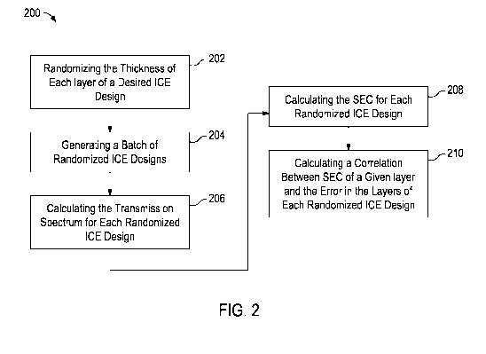
[0035] Referring to FIG. 2, illustrated is a schematic flowchart providing
an exemplary method 200 of evaluating an ICE design for fabrication, according
to one or more embodiments. Portions of the method 200 will be described with
reference to the exemplary desired ICE design shown in Table 1 below. As
indicated in Table 1, the desired ICE design encompasses a total of eight
layers,
and each layer has a different design layer thickness as determined by the
exemplary design process generally described above. It should be noted that
the exemplary desired ICE design in Table 1 is merely used for illustrative
purposes and therefore should not be considered limiting to the scope of this
disclosure.
Exemplary ICE Design
_ ¨
Laa_rit
Thickness (nm)
1 905.09
2 502.63
3 246.69
4 709.09
5 99.46
6 273.71
7 1206.40
8 1004.62
TABLE 1
[0036] In some embodiments, the method 200 may include
randomizing or otherwise altering the thickness of each layer of the desired
ICE
design, as at 202. Randomizing or altering the thickness of each layer may
simulate typical fabrication errors that may occur during the deposition
process
of physically fabricating each layer of the desired ICE design.
In some
embodiments, the randomized error applied to each layer could be entirely
"random," as generated or otherwise configured by the fabrication computer
CA 02896486 2015-06-25
WO 2014/130026 PCT/US2013/026894
program or another computational or physical device designed to generate a
sequence of thickness errors that lack any pattern.
[0037] In other embodiments, however, the randomized error applied
to each layer may follow a predetermined error iteration that changes the
design
thickness of each layer by a known thickness variance or certain percentage of
the design thickness for each layer (e.g., either an increase or decrease in
layer
thickness). For example, the design layer thickness of each layer of the
desired
ICE design may be varied by thickness variances of 1 nanometer (nm), 5 nm, 10
nm, etc., combinations thereof, fractions thereof, and the like. Similarly,
the
design thickness of each layer of the desired ICE design may be varied by 0.1%
of the design layer thickness, 0.5% of the design layer thickness, 1.0% of the
design layer thickness, 5.0% of the design layer thickness, etc., combinations
thereof, fractions thereof, and the like.
[0038] As will be appreciated, this process may result in the generation
of a plurality or "batch" of randomized ICE designs, as at 204, where each
randomized ICE design in the batch may have each layer thereof varied with
either a random or predetermined error variation. The resulting batch of
randomized ICE designs may include any number of randomized ICE designs as
set by an operator or computerized system. In some embodiments, for
example, a batch of randomized ICE designs may include 100 randomized ICE
designs. In other embodiments, a batch of randomized ICE designs may include
500, 1,000, or 10,000 randomized ICE designs, without departing from the
scope of the disclosure.
[0039] The method 200 may then proceed by calculating the
transmission spectrum for each of the randomized ICE designs, as at 206. As
known by those skilled in the art, such transmission spectra may be calculated
or otherwise generated using a computer system, such as a computer system
able to run the fabrication software program described above, or another
suitable computing program. Referring to FIG. 3, illustrated is a plot 300
that
depicts transmission spectra 302 for an exemplary randomized ICE design.
Specifically, the transmission spectra 302 correspond to a randomized ICE
design that has been randomized from the desired ICE design of Table 1 above.
As discussed below, by using the transmission spectra 302 of the randomized
ICE design, it may be possible to evaluate each individual layer thereof in an
11
CA 02896486 2015-06-25
WO 2014/130026 PCT/US2013/026894
effort to determine which layers are more sensitive than others to fabrication
error variations.
[0040] Referring again to FIG. 2, the method 200 may proceed by
calculating the chemometric SEC (or standard error of prediction (SEP)) for
each
randomized ICE design, as at 208. In
at least one embodiment, the
chemometric SEC for each randomized ICE design may be calculated by taking
the square root of the sum of squares between the known value for the analyte
of interest and the predicted value as derived from the transmission spectrum
of
the desired ICE design. This is accomplished for each randomized ICE design by
calculating its respective transmission spectrum and applying that
transmission
spectrum to the known data set of the analyte of interest. Such a calculation
of
an entire randomized ICE design in view of the original (error-free) desired
ICE
design may help determine how well a particular randomized ICE design will
perform with the randomized errors applied to each layer.
[0041] The method 200 may then include correlating the SEC (or SEP)
between a given layer and the error in the layers of each randomized ICE
design, as at 210. More particularly, the SEC may be calculated for each layer
between the error in each layer of each randomized ICE design and the
resulting
SEC degradation as compared with the corresponding layers of the desired
(error-free) ICE design (Table 1). In
some embodiments, a correlation
coefficient may be determined or otherwise obtained therefrom for each layer
of
the desired ICE design, and the correlation coefficient may be directly
proportional to how sensitive that layer may be to fabrication error. The
results
of such calculations may prove advantageous in determining which layers of the
desired ICE design are more sensitive to fabrication errors and would
therefore
result in large shifts in the transmission profile and decreases in overall
predictability.
[0042] Referring to FIG. 4, with continued reference to FIG. 3,
illustrated is a sensitivity plot 400 depicting the sensitivity of each layer
of the
randomized ICE design of FIG. 3. The sensitivity plot 400 may be generated by
comparing the transmission spectra 302 of FIG. 3 with the original
transmission
spectra of the desired (error-free) ICE design of Table 1, and the resulting
peaks
and valleys shown in the sensitivity plot 400 indicate sensitivity magnitude
of
each layer as corresponding to the respective error applied thereto.
12
CA 02896486 2015-06-25
WO 2014/130026 PCT/US2013/026894
[0043] A demarcation line 402 in the sensitivity plot 400 identifies a
series of "steps" corresponding to each contiguous layer of the randomized ICE
design. Specifically, as moving left to right in the sensitivity plot 400,
each step
extends across the respective thickness of each contiguous layer of the
randomized ICE design, as indicated on the x-axis. For example, the first step
(far left) of the demarcation line 402 corresponds to the first layer of the
randomized ICE design and encompasses a thickness of about 900 nm. The
second step (to the right of the first step) of the demarcation line 402
corresponds to the second layer of the randomized ICE design and has a
thickness of about 500 nm. The remaining steps (sequentially connected to the
right of the second step) of the demarcation line 402 correspond to the
remaining layers of the randomized ICE design, respectively, and otherwise
indicate the thickness of each layer, as represented on the x-axis.
Accordingly,
the overall thickness of the randomized ICE design is about 5000 nm.
[0044] As can be seen in the sensitivity plot 400, layers three, five, and
seven of the particular randomized ICE design appear to be more sensitive to
the applied error than the remaining layers. Moreover, layers four and eight
appear to be the least sensitive to the applied errors than the remaining
layers.
Similar sensitivity plots and determinations may be made for each randomized
ICE design of the batch of randomized ICE designs. A statistical analysis of
the
results from each sensitivity plot corresponding to each randomized ICE
design,
may indicate which layers of the desired ICE design (Table 1) may be more
sensitive to fabrication errors, thereby providing the correlation or
corresponding
correlation coefficient between the layer error and the resulting SEC
degradation. Results of such an analysis are depicted in FIG. 5.
[0045] Referring to FIG. 5, with continued reference to FIGS. 3 and 4,
illustrated is a fabrication sensitivity plot 500 corresponding to the desired
ICE
design of Table 1. In particular, the plot 500 provides SEC on the y-axis as a
function of each layer of the desired ICE design, as shown on the x-axis. Each
point in the plot 500 represents an average SEC value for the indicated layer
of
the desired ICE design as derived from the corresponding layers of each
randomized ICE design.
In other words, the sensitivity plots for each
randomized ICE design (i.e., similar to the sensitivity plot 400 of FIG. 4)
were
combined and the sensitivity of each layer in view of the applied error was
averaged in order to determine the average sensitivity of each respective
layer.
13
CA 02896486 2015-06-25
WO 2014/130026 PCT/US2013/026894
From the average sensitivity of each layer of the randomized ICE designs, the
average SEC of the respective layers could be determined and otherwise
depicted in the fabrication sensitivity plot 500.
[0046] As shown in the plot 500, the sixth and eight layers report
having the least effect on SEC as opposed to the remaining layers. In other
words, fabrication errors in the sixth and eight layers will likely have
little or
negligible detrimental impact on the overall SEC of the desired ICE design. On
the other hand, the third and fifth layers report having the most effect on
SEC as
opposed to the remaining layers. As a result, fabrication errors in the third
and
fifth layers will likely have a greater negative impact on the overall SEC of
the
desired ICE design than the remaining layers. Accordingly, the plurality of
layers
of the desired ICE design have been effectively ranked based on the
sensitivity
to changes in the standard error of calibration. In accordance with such
ranking,
the third and fifth layers of the desired ICE design may be characterized or
otherwise treated as sensitive or hypersensitive layers of the desired ICE
design.
[0047] Once an operator knows which of the layers of a desired ICE
design will be more sensitive to fabrication errors than others, the care with
which each layer is deposited may be set depending on the effect that a
particular layer may have on the final chemometric predictability (SEC or
SEP).
In some embodiments, for example, the deposition of more sensitive layers may
be set by slowing the deposition rate and thereby ensuring accurate and
precise
deposition of such layers during the fabrication process. In other
embodiments,
or otherwise in addition thereto, the deposition of more sensitive layers may
be
set by programming or otherwise undertaking various optical measurements
(e.g., analyzing the transmission profile) during the fabrication process of
such
sensitive layers to ensure that the deposition thickness does not overshoot or
otherwise undershoot the original design parameters for the desired ICE
design.
For instance, optical measurements may be taken at predetermined deposited
thicknesses of the sensitive layers, such as by taking optical measurements at
50%, 60%, 70%, 80%, 90%, 95%, etc. of the total layer deposition. Those
skilled in the art will readily recognize that the optical measurements may be
taken at other percentages of the total layer deposition, without departing
from
the scope of the disclosure. In other words, additional precision, accuracy,
or
focus on the part of the operator may be necessary or otherwise recommended
in setting the layers that are more susceptible to causing SEC degradation.
14
CA 02896486 2015-06-25
WO 2014/130026 PCT/US2013/026894
[0048] The methods disclosed herein may also prove advantageous in
helping an operator make fabrication decisions. For instance, the disclosed
methods may help an operator determine if a particular desired ICE design
contains hypersensitive layers in which small deposition layer errors may be
capable of degrading chemometric predictability to a point where the desired
ICE
design would be rendered useless or otherwise ineffective for its intended
purpose. In such cases, the operator may be able to intelligently determine if
a
desired ICE design is a viable design in terms of reproducible predictability
or its
ability to provide a reproducible transmission profile. Desired ICE designs
that
are determined to be non-viable may be discarded entirely prior to expending
the time and resources in fabricating the same.
[0049] The methods disclosed herein may also help an operator
determine which desired ICE design is more preferred over other desired ICE
designs. For example, the final fabricated batch of ICE components following a
manufacturing run will likely contain ICE components that are predictive,
despite
exhibiting spectral shifts attributable to fabrication layer errors.
Using the
presently disclosed methods, however, the operator may be able to
intelligently
determine which batch of a desired ICE design would be more desirable than
another due to a lower average batch SEC. As a result, the batch of the chosen
desired ICE design will result in a higher yield of predictive ICE components.
[0050] Those skilled in the art will readily appreciate that the methods
described herein, or large portions thereof, may be automated at some point
such that a computerized system may be programmed to design, predict, and
fabricate ICE components that are more robust for fluctuating extreme
environments. Computer hardware used to implement the various methods and
algorithms described herein can include a processor configured to execute one
or
more sequences of instructions, programming stances, or code stored on a non-
transitory, computer-readable medium. The processor can be, for example, a
general purpose microprocessor, a microcontroller, a digital signal processor,
an
application specific integrated circuit, a field programmable gate array, a
programmable logic device, a controller, a state machine, a gated logic,
discrete
hardware components, an artificial neural network, or any like suitable entity
that can perform calculations or other manipulations of data.
In some
embodiments, computer hardware can further include elements such as, for
example, a memory (e.g., random access memory (RAM), flash memory, read
CA 02896486 2015-06-25
-
WO 2014/130026
PCT/US2013/026894
only memory (ROM), programmable read only memory (PROM), electrically
erasable programmable read only memory (EEPROM)), registers, hard disks,
removable disks, CD-ROMS, DVDs, or any other like suitable storage device or
medium.
[0051] Executable sequences described herein can be implemented with
one or more sequences of code contained in a memory. In some embodiments,
such code can be read into the memory from another machine-readable
medium. Execution of the sequences of instructions contained in the memory
can cause a processor to perform the process steps described herein. One or
more processors in a multi-processing arrangement can also be employed to
execute instruction sequences in the memory. In addition, hard-wired circuitry
can be used in place of or in combination with software instructions to
implement various embodiments described herein.
Thus, the present
embodiments are not limited to any specific combination of hardware and/or
software.
[0052] As used herein, a machine-readable medium will refer to any
medium that directly or indirectly provides instructions to a processor for
execution. A machine-readable medium can take on many forms including, for
example, non-volatile media, volatile media, and transmission media. Non-
volatile media can include, for example, optical and magnetic disks. Volatile
media can include, for example, dynamic memory. Transmission media can
include, for example, coaxial cables, wire, fiber optics, and wires that form
a
bus. Common forms of machine-readable media can include, for example,
floppy disks, flexible disks, hard disks, magnetic tapes, other like magnetic
media, CD-ROMs, DVDs, other like optical media, punch cards, paper tapes and
like physical media with patterned holes, RAM, ROM, PROM, EPROM and flash
EPROM.
[0053] Therefore, the present invention is well adapted to attain the
ends and advantages mentioned as well as those that are inherent therein. The
particular embodiments disclosed above are illustrative only, as the present
invention may be modified and practiced in different but equivalent manners
apparent to those skilled in the art having the benefit of the teachings
herein.
Furthermore, no limitations are intended to the details of construction or
design
herein shown, other than as described in the claims below. It is therefore
evident that the particular illustrative embodiments disclosed above may be
16
CA 02896486 2015-06-25
WO 2014/130026 PCT/US2013/026894
altered, combined, or modified and all such variations are considered within
the
scope and spirit of the present invention. The invention illustratively
disclosed
herein suitably may be practiced in the absence of any element that is not
specifically disclosed herein and/or any optional element disclosed herein.
While
compositions and methods are described in terms of "comprising," "containing,"
or "including" various components or steps, the compositions and methods can
also "consist essentially of" or "consist of" the various components and
steps.
All numbers and ranges disclosed above may vary by some amount. Whenever
a numerical range with a lower limit and an upper limit is disclosed, any
number
and any included range falling within the range is specifically disclosed. In
particular, every range of values (of the form, "from about a to about b," or,
equivalently, "from approximately a to b," or, equivalently, "from
approximately
a-b") disclosed herein is to be understood to set forth every number and range
encompassed within the broader range of values. Also, the terms in the claims
have their plain, ordinary meaning unless otherwise explicitly and clearly
defined
by the patentee. Moreover, the indefinite articles "a" or "an," as used in the
claims, are defined herein to mean one or more than one of the element that it
introduces. If there is any conflict in the usages of a word or term in this
specification and one or more patent or other documents that may be
incorporated herein by reference, the definitions that are consistent with
this
specification should be adopted.
17