Note : Les descriptions sont présentées dans la langue officielle dans laquelle elles ont été soumises.
CA 02896654 2015-06-25
WO 2014/120850
PCT/US2014/013707
APPARATUS AND METHODS FOR FEEDBACK
SENSING IN MULTI-CELL POWER SUPPLIES
BACKGROUND
This invention relates to multi-cell power
supplies. More particularly, this invention relates to
apparatus and methods for feedback sensing in multi-cell
power supplies.
SUMMARY
In a first aspect of the invention, a multi-cell
power supply is provided for receiving power from a source
and delivering power at an output terminal to a load. The
multi-cell power supply includes a first power cell
coupled to the source, and a first current sensor circuit.
The first power cell provides a first output current, and
includes a first output terminal coupled to a reference
node of the multi-cell power supply, and a second output
terminal coupled to the output terminal. The first
current sensor circuit includes a first current sensor and
a power supply. The first current sensor is coupled to
the first output terminal of the first power cell, and
measures the first output current. The power supply is
coupled to either the reference node or a floating ground
node of the first power cell, and provides power to the
first current sensor.
In a second aspect of the invention, a multi-cell
power supply is provided for receiving power from a source
and delivering power at an output terminal to a load. The
multi-cell power supply includes a first power cell
coupled to the source. The first power cell includes a
first output terminal coupled to a reference node of the
multi-cell power supply, a second output terminal coupled
1
CA 02896654 2015-06-25
WO 2014/120850 PCT/US2014/013707
to the output terminal, and a first resistor network, a
second resistor network, and a floating ground node. The
first resistor network is coupled between the first output
terminal of the first power cell and the floating ground
node of the first power cell. The second resistor network
is coupled between the second output terminal of the first
power cell and the floating ground node of the first power
cell. The first resistor network provides a first
feedback voltage of the first power cell, and the second
resistor network provides a second feedback voltage of the
first power cell.
In a third aspect of the invention, a method is
provided for use with a multi-cell power supply that
receives power from a source and delivers power at an
output terminal to a load. The method includes:
(a) coupling a first power cell to the source, the first
power cell providing a first output current; (b) coupling
a first output terminal of the first power cell to a
reference node of the multi-cell power supply;
(c) coupling a second output terminal of the first power
cell to the output terminal; (d) coupling a first current
sensor circuit to the first power cell, the first current
sensor circuit including a first current sensor and a
power supply; (e) coupling the first current sensor to the
first output terminal of the first power cell;
(f) coupling the power supply of the first current sensor
circuit to either the reference node or a floating ground
node of the first power cell, wherein the power supply of
the first current sensor circuit provides power to the
first current sensor; and (g) using the first current
sensor to measure the first output current.
Other features and aspects of the present invention
will become more fully apparent from the following
2
CA 02896654 2015-06-25
WO 2014/120850 PCT/US2014/013707
detailed description, the appended claims and the
accompanying drawings.
BRIEF DESCRIPTION OF THE DRAWINGS
Features of the present invention can be more
clearly understood from the following detailed description
considered in conjunction with the following drawings, in
which the same reference numerals denote the same elements
throughout, and in which:
FIG. 1A is a block diagram of a previously known
multi-cell power supply;
FIG. 1B is a more detailed block diagram of the
previously known multi-cell power supply of FIG. 1A;
FIG. 2 is a block diagram of an example multi-cell
power supply in accordance with this invention;
FIG. 3A is a block diagram of an example power
circuit of the multi-cell power supply of FIG. 2;
FIG. 3B is a block diagram of an alternative
example power circuit of the multi-cell power supply of
FIG. 2;
FIG. 3C is a block diagram of another alternative
example power circuit of the multi-cell power supply of
FIG. 2;
FIG. 4A is a block diagram of an example current
sensor circuit and power cell of the multi-cell power
supply of FIG. 2;
FIG. 4B is a block diagram of an alternative
example current sensor circuit and power cell of the
multi-cell power supply of FIG. 2;
FIG. 5 is a block diagram of an alternative example
multi-cell power supply in accordance with this invention;
FIG. 6 is a block diagram of an example power
circuit of the multi-cell power supply of FIG. 5; and
3
CA 02896654 2016-08-11
54106-1875
FIG. 7 is a block diagram of an example power cell
of the multi-cell power supply of FIG. 5.
DETAILED DESCRIPTION
Previously known multi-cell power supplies, such as
described in Hammond U.S. Patent No. 5,625,545, Aiello et
al. U.S. Patent No. 6,014,323, Hammond U.S. Patent
No. 6,166,513, Rastogi et al. U.S. Patent No. 7,508,147,
and Hammond et al. U.S. Patent No. 8,169,107, use modular
power cells to deliver medium-voltage power to a load,
such as a three-phase AC motor.
As used herein, a "medium voltage" is a voltage of
greater than about 690V and less than about 69kV, and a
"low voltage" is a voltage less than about 690V. Persons
of ordinary skill in the art will understand that other
voltage levels may be specified as "medium voltage" and
"low voltage." For example, in some embodiments, a
"medium voltage" may be a voltage between about lkV and
about 69kV, and a "low voltage" may be a voltage less than
about lkV.
For example, FIGS. 1A-1B illustrate a previously
known multi-cell power supply 10 that receives three-phase
power from an AC source, and delivers power to a load 12
(e.g., a three-phase AC motor). As shown in FIG. 1A,
multi-cell power supply 10 includes a transformer 14, a
power circuit 16, a controller 18, a current sensor 20 and
a resistor network that includes resistors R1 and R2.
As shown in FIG. IB, transformer 14 includes a
primary winding 14p that excites nine secondary
windings 14s1-14s9, and power circuit 16 includes power
cells 16al, 16b1, . . 16c3 that are coupled to
4
CA 02896654 2015-06-25
WO 2014/120850
PCT/US2014/013707
secondary windings 14s1-14s9, respectively, of
transformer 14. Power cells 16a1, 16b1, . . ., 16c3 are
configured to provide medium voltage output power to
load 12.
In particular, each output phase of power
circuit 16 is fed by a group of series-connected power
cells 16a1, 16b1, . . ., 16c3. Power cells 16a1, 16a2
and 16a3 are coupled in series in a first phase group,
power cells 16b1, 16b2 and 16b3 are coupled in series in a
second phase group, and power cells 16c1, 16c2 and 16c3
are coupled in series in a third phase group. Each phase
output voltage is the sum of the output voltages of the
power cells in the phase group. For example, if each of
power cells 16a1, 16b1, . . ., 16c3 has a maximum output
voltage magnitude of about 600V, each phase of power
circuit 16 can produce a maximum output voltage magnitude
of about 1800V above neutral. In this regard, power
circuit 16 delivers medium voltage power to load 12 using
power cells 16a1, 16b1, . . ., 16c3 that include
components rated for voltages substantially lower than the
rated output voltage.
Each of power cells 16a1, 16b1, . . ., 16c3 is
coupled (e.g., via an optical fiber communication link) to
controller 18, which uses current feedback and voltage
feedback to control the operation of power cells 16a1,
16b1, . . ., 16c3. In particular, current sensors 20b
and 20c sense the output current of power circuit 16, and
provide output signals corresponding to the sensed
currents to controller 18. The current corresponding to
phase A is determined by the equation:
iA = - iB - iC
Current sensors 20b and 20c each may include a
Hall-effect transducer that is coupled to a low voltage
5
CA 02896654 2015-06-25
WO 2014/120850 PCT/US2014/013707
supply (e.g., 15V), and provides a low voltage output
signal proportional to the measured current. The low
voltage supplies and output signals of current sensors 20b
and 20c are directly connected to controller 18. Thus,
current sensors 20b and 20c require isolation for rated
output line-to-ground voltage (e.g., 2400V) for normal
operation, and isolation for rated line-to-line voltage
(e.g., 4160V) for operation under ground fault.
Commercially available current sensors, however,
typically do not have such high isolation ratings. As a
result, previously known multi-cell power supplies
typically use special techniques to provide medium voltage
isolation for current sensors 20b and 20c, such as using
shielded cables through the current sensors. Such
techniques require current sensors with large apertures to
accommodate the larger conductor size of shielded cables,
which increases the cost and complexity of current sensor
implementation.
In addition, resistors R1 and R2 are coupled to the
output bus of power circuit 16, and provide voltage
feedback to controller 18. Typically, R2 >> R1, such that
the attenuated feedback voltage signal is much smaller
than the rated output voltage of power circuit 16. For
example, R1 may be about 4.8 kO, and R2 may be between
about 1.7 MO to about 21 MO depending on the required
output voltage of multi-cell power supply 10. To avoid
obscuring the drawing, a single set of resistors R1 and R2
are shown coupled to a single phase output of power
circuit 16 in FIG. 1B. Typically, separate sets of
resistors R1 and R2 are coupled to each output phase of
power circuit 16.
Resistor R2 typically is implemented using high
voltage resistors, including multiple series-coupled
resistors to mitigate the potential effect of failures.
6
CA 02896654 2015-06-25
WO 2014/120850
PCT/US2014/013707
High voltage resistors are bulky, and the resistor network
including R1 and R2 requires special testing to qualify
for high voltage operation, and requires a dedicated space
in the high voltage section of multi-cell power supply 10.
In addition, because multi-cell power supply 10 may be
used to provide a range of output voltages, different R2
values must be used depending on the required output
voltage.
Further, the high voltage connections to
resistor R2, and the low voltage feedback connections to
resistor R1 and controller 18 require careful routing
through cabinets where high voltages are present. Such
routing of low voltage wiring can introduce noise into the
feedback signals. All of these factors increase the cost
and complexity of implementing voltage sensing using
attenuator resistors.
Apparatus and methods in accordance with this
invention provide current feedback for multi-cell power
supplies using current sensor circuits that are powered by
and coupled to the power cell whose current is being
measured. In accordance with this invention, such current
sensor circuits require isolation for the rated voltage of
the power cell, and do not require isolation for the rated
output line-to-ground voltage or rated line-to-line
voltage of the power supply.
In addition, apparatus and methods in accordance
with this invention provide voltage feedback for multi-
cell power supplies using power cells that each include
resistor networks coupled between the output terminals of
the power cell, and a floating ground terminal of the
power cell. The resistor network in each power cell
provides voltage feedback signals for the power cell. The
voltage feedback signals for each power cell in a phase
group may be added to determine a voltage feedback signal
7
CA 02896654 2015-06-25
WO 2014/120850 PCT/US2014/013707
for the phase group. As a result, the resistor networks
in each power cell may use conventional resistors rather
than the high voltage resistors required in previously
known multi-cell power supplies.
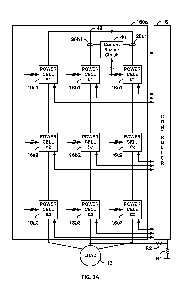
Referring now to FIG. 2, an example multi-cell
power supply 100a in accordance with this invention is
described. Multi-cell power supply 100a includes
transformer 14, a power circuit 160, controller 18 and
feedback resistors R1 and R2. As described in more detail
below, unlike previously known multi-cell power supply 10
of FIG. 1A, multi-cell power supply 100a does not include
current sensor 20 coupled to the output bus of power
circuit 160.
Referring now to FIG. 3A, an example embodiment of
power circuit 160 is described. Power circuit 160a
includes nine power cells 16a1, 16b1, . . ., 16c3 that are
coupled to transformer 14 (to avoid obscuring the drawing,
transformer 14 is not shown) and are coupled via
communication links to controller 18. Persons of ordinary
skill in the art will understand that more or less than
nine power cells 16a1, 16b1, . . ., 16c3 may be used. In
addition, persons of ordinary skill in the art will
understand that transformer 14 may include different
configurations of primary winding 14p and secondary
windings 14s1-14s9, and may include more or less than nine
secondary windings 14s1-14s9 than those depicted in
FIG. 1B.
Each output phase of power circuit 160a is fed by a
group of series-connected power cells 16a1, 16b1, . . .,
16c3. Power cells 16a1, 16a2 and 16a3 are coupled in a
first phase group, power cells 16b1, 16b2 and 16b3 are
coupled in a second phase group, and power cells 16c1,
16c2 and 16c3 are coupled in a third phase group, with the
three phase groups joined in a WYE connection at reference
8
CA 02896654 2015-06-25
WO 2014/120850 PCT/US2014/013707
node 42. Persons of ordinary skill in the art will
understand that more or less than three output phases may
be used.
Power circuit 160a also includes a current sensing
circuit 40 that is coupled to current sensors 20b1
and 20c1, power cell 16c1, controller 18 and reference
node 42. Current sensors 20b1 and 20c1 may be any
conventional current sensors, such as LT 2005-S current
transducers by LEM Holding SA, Geneva, Switzerland.
Persons of ordinary skill in the art will understand that
other current sensors may be used. Current sensors 20b1
and 20c1 are adjacent reference node 42, and each have
power terminals p and provide a measurement output signal
at output terminal m.
Referring now to FIG. 4A, an example current sensor
circuit 40 is described. Current sensor circuit 40
includes a power supply 44, a processor 46 and a fiber
optic interface 48. Power supply 44 includes a first
input signal coupled to one or more phases of the three-
phase input to power cell 16c1, and a second input signal
coupled to reference node 42, and provides power
(e.g., 15VDC) to power terminals p of current
sensors 20b1 and 20c1. Power supply 44 may be any
conventional AC-DC converter or other similar power
supply.
Processor 46 has input terminals coupled to output
terminals m of current sensors 20b1 and 20c1, and has an
output terminal coupled to fiber optic interface 48.
Processor 46 provides the measured output signals from
current sensors 20b1 and 20c1 to controller 18 via fiber
optic interface 48. Processor 46 may be a microprocessor,
such as a 1M5320F2801 processor by Texas Instruments,
Dallas, TX, a Programmable Gate Array device (such as FPGA
from Altera or Xilinx) that can be configured to perform
9
CA 02896654 2015-06-25
WO 2014/120850
PCT/US2014/013707
the functions of a processor, an op-amp based circuit with
a V/f converter to transmit the sensed feedback over
fiber-optics, or other similar processor or circuit.
Fiber optic interface 48 is coupled between processor 46
and controller 18, and provides electrical isolation
between current sensor circuit 40 and controller 18.
Fiber optic interface 48 may be an AFBR 2624Z/AFBR 1624Z
fiber optic receiver/transmitter pair by Avago
Technologies, San Jose, CA, or may be any other similar
fiber optic interface.
Power cell 16c1 may be a conventional power cell
that includes a rectifier 50, DC bus capacitor(s) 52, an
inverter 54, a processor 56, and a fiber optic
interface 58. Rectifier 50 converts the three-phase input
AC signal to a substantially constant DC voltage coupled
to DC bus capacitor(s) 52. Inverter 54 converts the DC
voltage across DC bus capacitor(s) 52 to an AC output.
Rectifier 50, DC bus capacitor(s) 52, and inverter 54 have
a common floating ground node. A first output terminal of
power cell 16c1 is coupled to reference node (WYE
connection) 42, and a second output terminal of power
cell 16c1 is coupled to power cell 16c2 (not shown in
FIG. 4A).
Processor 56 may be coupled to controller 18 via
fiber optic interface 58. Processor may be a TM5320F2801
processor, or may be any other similar processor. Fiber
optic interface 58 may be an AFBR 2624Z/AFBR 1624Z fiber
optic receiver/transmitter pair, or may be any other
similar fiber optic interface. Processor 56 may
communicate status information regarding power cell 16c1
to controller 18, and controller 18 may communicate
control signals to processor 56 to control operation of
power cell 16c1.
CA 02896654 2015-06-25
WO 2014/120850
PCT/US2014/013707
Current sensor 20b1 is coupled between the first
output terminal of power cell 16b1 and reference node 42,
current sensor 20c1 is coupled between the first output
terminal of power cell 16c1 and reference node 42, and
power supply 44 is coupled to reference node 42. This
equalizes the isolation voltage stress on current
sensors 20b1 and 20c1.
In addition, the isolation requirement for each of
current sensors 20b1 and 20c1 equals the rated output
voltage of power cell 16c1 (e.g., 480V). In contrast,
current sensors 20b and 20c of previously known multi-cell
power supply 10 of FIGS. 1A-1B, require isolation for the
rated output-to-ground voltage (e.g., 2400V) during normal
operation or require isolation for the rated line-line
voltage of multi-cell power supply 10 (e.g., 4160V) during
abnormal operation such as under an output ground fault
condition. Thus, the isolation requirement for current
sensors 20b1 and 20c1 is much lower than that required for
current sensors 20b and 20c of previously known multi-cell
power supply 10. In addition, the isolation requirement
for current sensors 20b1 and 20c1 is not affected by the
rated output voltage of multi-cell power supply 100a, or
by the size of the shielded conductor used on the output
bus of multi-cell power supply 100a.
In accordance with this invention, current
sensor 20b1 measures an output current of power cell 16b1,
and current sensor 20c1 measures an output current of
power cell 16c1. The measured output current of power
cell 16b1 substantially equals the "b" phase output
current of power circuit 160a, and the measured output
current of power cell 16c1 substantially equals the "c"
phase output current of power circuit 160a. Thus, power
circuit 160a provides current feedback to controller 18
11
CA 02896654 2015-06-25
WO 2014/120850 PCT/US2014/013707
without requiring high voltage isolation of current
sensors 20b1 and 20c1.
Referring now to FIG. 3B, an alternative example
embodiment of power circuit 160 is described. In
particular, power circuit 160b includes a first current
sensor circuit 40b1 coupled to current sensor 20b1 and
power cell 16b1, and a second current sensor circuit 40c1
coupled to current sensor 20c1 and power cell 16c1. In
this regard, each of current sensors 20b1 and 20c1 is
powered by the source supplying the corresponding power
cell, and measures an output current of power cells 16b1
and 16c1, respectively.
Referring now to FIG. 4B, an example current sensor
circuit 40c1 is described. Current sensor circuit 40c1
includes power supply 44, which has a first input signal
coupled to one or more phases of the three-phase input to
power cell 16c1, a second input signal coupled to the
floating ground of power cell 16c1, and provides power
(e.g., 15VDC) to power terminals p of current
sensor 20c1. Output terminal m of current sensor 20c1 is
coupled to an input terminal of processor 56 of power
cell 16c1.
Processor 56 provides the measured output signal
from current sensor 20c1 to controller 18 via fiber optic
interface 58. In this regard, second current sensor
circuit 40c1 does not require its own dedicated processor
and fiber optic link, but instead uses the existing
processor 56 and fiber optic link 58 of power cell 16c1 to
communicate the measured output signal of current
sensor 20c1 to controller 18. Although not shown in
FIG. 4B, first current sensor circuit 40b1 may be the same
as second current sensor circuit 40c1, and may use the
processor and fiber optic link of power cell 16b1 to
communicate the measured output signal of current
12
CA 02896654 2015-06-25
WO 2014/120850
PCT/US2014/013707
sensor 20b1 to controller 18. The isolation requirement
for each of current sensors 20b1 and 20c1 in FIG. 3B
equals the rated output voltage of power cells 16b1
and 16c1, respectively (e.g., 480V).
In accordance with this invention, current
sensor 20b1 measures an output current of power cell 16b1,
and current sensor 20c1 measures an output current of
power cell 16c1. The measured output current of power
cell 16b1 substantially equals the "b" phase output
current of power circuit 160b, and the measured output
current of power cell 16c1 substantially equals the "c"
phase output current of power circuit 160a. Thus, power
cells 16b1 and 16c1 provide current feedback to
controller 18 without requiring high voltage isolation
corresponding to the rated voltage of the power circuit
(e.g., 2400V).
Power cells in accordance with this invention may
include more than two current sensors. For example,
referring now to FIG. 3C, another alternative example
embodiment of power circuit 160 is described. In
particular, power circuit 160c includes current sensor
circuits 40a1, 40b1, . . ., 40b3, 40c3 coupled to
corresponding power cells 16a1, 16b1, . . ., 16b3, 16c3,
respectively, and corresponding current sensors 20a1,
20b1, . . ., 20b3, 20c3, respectively.
In this regard, each current sensor 20a1, 20b1, . .
., 20b3, 20c3 is powered by and measures an output current
of corresponding power cells 16a1, 16b1, . . ., 16b3,
16c3, respectively. In addition, power cells 16a1, 16b1,
. . ., 16b3, 16c3 are used to communicate the measured
output signals of corresponding current sensors 20a1,
20b1, . . ., 20b3, 20c3, respectively, to controller 18.
Such a configuration may be used to provide redundancy for
current sensing. As in the embodiments of FIGS. 3A
13
CA 02896654 2015-06-25
WO 2014/120850
PCT/US2014/013707
and 3B, the isolation requirement for each of current
sensors 20a1, 20b1, . . ., 20b3, 20c3 in FIG. 3C equals
the rated output voltage of corresponding power
cells 16a1, 16b1, . . ., 16b3, 16c3, respectively
(e.g., 480V).
Persons of ordinary skill in the art will
understand that separate current sensors 20a1,
20b1, . . ., 20b3, 20c3 and current sensor circuits 40a1,
40b1, . . ., 40b3, 40c3 may be used with all or fewer than
all of power cells power cells 16a1, 16b1, . . ., 16b3,
16c3 depending on the amount of redundancy desired.
Referring now to FIG. 5, an alternative example
multi-cell power supply 100b in accordance with this
invention is described. Multi-cell power supply 100b
includes transformer 14, a power circuit 260 and
controller 18. As described in more detail below, unlike
previously known multi-cell power supply 10 of FIG. 1A,
and example multi-cell power supply 100a of FIG. 2, multi-
cell power supply 100b does not include resistors R1
and R2 coupled to the output bus of power circuit 260.
Referring now to FIG. 6, an example embodiment of
power circuit 260 is described. Power circuit 260
includes nine power cells 16a1', 16b1', . . ., 16c3' that
are coupled to transformer 14 (to avoid obscuring the
drawing, transformer 14 is not shown) and also are coupled
via communication links to controller 18. Persons of
ordinary skill in the art will understand that more or
less than nine power cells 16a1', 16b1', . . ., 16c3' may
be used. Persons of ordinary skill in the art will
understand that transformer 14 may include different
configurations of primary winding 14p and secondary
windings 14s1-14s9, and may include more or less than nine
secondary windings 14s1-14s9 than those depicted in
FIG. 1B.
14
CA 02896654 2015-06-25
WO 2014/120850 PCT/US2014/013707
Each output phase of power circuit 260 is fed by a
group of series-connected power cells 16a1', 16b1', . . .,
16c3'. Power cells 16a1', 16a2' and 16a3' are coupled in
a first phase group, power cells 16b1', 16b2' and 16b3'
are coupled in a second phase group, and power
cells 16c1', 16c2' and 16c3' are coupled in a third phase
group, with the three phase groups joined in a WYE
connection with a reference node 42. Persons of ordinary
skill in the art will understand that more or less than
three output phases may be used.
In addition, a first current sensor circuit 40b1 is
coupled to current sensor 20b1 and power cell 16b1', and a
second current sensor circuit 40c1 is coupled to current
sensor 20c1 and power cell 16c1'. In this regard, each of
current sensors 20b1 and 20c1 is powered by the input
source supplying the power cells, and measures an output
current of power cells 16b1' and 16c1', respectively.
Persons of ordinary skill in that art will understand that
current sensors 20b1 and 20c1 alternatively may be coupled
to a single power cell 16b1' (such as in the embodiment of
FIG. 3A). Likewise, separate current sensor 20a1,
20b1, . . ., 20b3 and 20c3 alternatively may be powered by
corresponding power cells 16a1', 16b1', . . ., 16b3'
and 16c3', respectively, (such as in the embodiment of
FIG. 3C).
Referring now to FIG. 7, an example power
cell 16c1' is described. Power cell 16c1' is similar to
power cell 16c1 of FIG. 4A, but also includes a first
resistor network R1a' and R2a' coupled between a first
output terminal of inverter 54 and the floating ground
node of power cell 16c1', and a second resistor
network Rib' and R2b' coupled between a second output
terminal of inverter 54 and the floating ground node of
power cell 16c1'.
CA 02896654 2015-06-25
WO 2014/120850
PCT/US2014/013707
First resistor network R1a' and R2a' provides a
first voltage feedback signal Vc1a to processor 56, and
second resistor network Rib' and R2b' provides a second
voltage feedback signal Vc1b to processor 56.
Processor 56 communicates the voltage feedback
signals Vc1a and Vc1b to controller 18 via fiber optic
interface 58. For power cells that have a uni-polar
output with one of the two terminals as a reference node,
a single resistor network of R1a' and R2a' is sufficient
to provide voltage feedback.
Referring again to FIG. 6, each of power
cells 16a1', 16b1', . . ., 16b3', 16c3' similarly
communicates corresponding voltage feedback signals to
controller 18, which reconstructs the total voltage
feedback signal of power circuit 260 by summing the
individual voltage feedback signals from power
cells 16a1', 16b1', . . ., 16b3' and 16c3'. For example,
the voltage feedback signals for each phase may be
determined as:
VFBA = (Va1a ¨ Va1b) + (Va2a ¨ Va2b) + (Va3a ¨ Va3b) (1)
VFBB = (Vb1a ¨ Vb1b) + (Vb2a ¨Vb2b) + (Vb3a ¨ Vb3b) (2)
VFBC = (Vc1a ¨ Vc1b) + (Vc2a ¨Vc2b) + (Vc3a ¨ Vc3b) (3)
where Va1a and Va1b are the voltage feedback signals of
power cell 16a1', Va2a and Va2b are the voltage feedback
signals of power cell 16a2', Va3a and Va3b are the voltage
feedback signals of power cell 16a3', Vb1a and Vb1b are
the voltage feedback signals of power cell 16b1', Vb2a
and Vb2b are the voltage feedback signals of power
cell 16b2', Vb3a and Vb3b are the voltage feedback signals
of power cell 16b3', Vc1a and Vc1b are the voltage
feedback signals of power cell 16c1', Vc2a and Vc2b are
the voltage feedback signals of power cell 16c2', and Vc3a
16
CA 02896654 2015-06-25
WO 2014/120850
PCT/US2014/013707
and Vc3b are the voltage feedback signals of power
cell 16c3'.
Referring again to FIG. 7, because first resistor
network R1a' and R2a', and second resistor network Rib'
and R2b' are each coupled between an output terminal of
inverter 54 and the floating ground node of power
cell 16c1', resistors R1a', R2a', Rib' and R2b' may be
sized based on the fixed rated output voltage of power
cell 16c1' (e.g., 480V). For example, R1a' and Rib' each
may be about 4.8 kO, and R2a' and R2b' each may be between
about 300 kO to about 1 MO, depending on the rated voltage
of power cell 16c1'.
As a result, R2a' and R2b' may be more easily
obtainable, and at lower cost than resistor R2 used in
previously known multi-cell power supply 10. Further,
whereas multiple values of resistor R2 are required
depending on the rated output voltage of previously known
multi-cell power supply 10, in example multi-cell power
supply 100b of FIG. 5, a single value of resistors R2a'
and R2b' is required based on the fixed rated voltage of
the power cells 16a1', 16b1', . . ., 16b3' and 16c3'.
Moreover, isolation between the controller 18 and the
output voltage of multi-cell power supply 100b is achieved
through the existing fiber optic communication links
within each of power cells 16a1', 16b1', . . ., 16b3'
and 16c3' without the need for additional circuitry or
components.
The foregoing merely illustrates the principles of
this invention, and various modifications can be made by
persons of ordinary skill in the art without departing
from the scope and spirit of this invention.
For example, modular medium voltage power supplies
in accordance with this invention utilize H-bridge
inverters as a modular component in the power cell that is
17
CA 02896654 2015-06-25
WO 2014/120850
PCT/US2014/013707
connected in series to form the medium voltage output.
Other power supply circuits use different structures for
the modular component, such as half-bridge inverters or
neutral-point clamped inverters to provide a medium
voltage output. Current sensor circuit implementation in
accordance with this invention may be incorporated into
these power supply circuits to provide the same advantages
of lower complexity and cost.
In addition, power supplies in accordance with this
invention may be coupled between a source and a load, and
may provide uni-directional or bi-directional power flow
between the two.
18