Note : Les descriptions sont présentées dans la langue officielle dans laquelle elles ont été soumises.
CA 02898692 2015-07-20
WO 2014/128519 PCT/1B2013/000421
1
A connection system and
an ultrasound system comprising said connection system
FIELD OF THE INVENTION
The present invention concerns a connection system
for connecting a probe to an electronic device in an
ultrasound system.
BACKGROUND OF THE INVENTION
The present invention concerns more precisely a
connection system for connecting a probe to an electronic
device, wherein the probe emits and/or receives ultrasound
waves into a medium, and wherein the connection system
comprises:
- a first element (a receptacle) having first
electrical contacts, said first element being attached to
the electronic device,
- a second element (a connector) having second
electrical contacts for providing an electrical connection
between the first electrical contacts and the second
electrical contacts, said second element being attached to
the probe,
- an activation device, and
- a third element that can be moved by the
activation device relative to the first element between an
activated position and an inactivated position, wherein in
the activated position the first electrical contacts can
contact the second electrical contacts, and in the
inactivated position the first electrical contacts can not
contact the second electrical contacts.
It is known from the document US 5 882 310 a
connection system adapted for a multiport ultrasound
imaging system. The imaging system comprises a plurality of
receptacles that receives a probe connector, each
receptacle having a plate that is actuated by a pressure
roller to rotate the receptacle contacts to the probe
CA 02898692 2015-07-20
WO 2014/128519 PCT/1B2013/000421
2
connector contacts.
Only one receptacle can be activated at the same
time, and only one probe is connected to the ultrasound
imaging system. The connection system eliminates the need
of having switches inside the imaging system to select a
specific ultrasound probe. Such connection system is
advantageous in terms of size and cost.
However, this connection system is able connect
only one connector to the imaging system at the same time.
The imaging system needs to be powered to mechanically
disconnect and remove a connected probe. The probe can not
be easily and rapidly disconnected and removed from the
electronic device.
OBJECTS AND SUMMARY OF THE INVENTION
One object of the present invention is to provide a
connection system that also eliminate the switches inside
the ultrasound system, and that is improved so as it is
possible to easily mechanically connect or disconnect the
probe from the ultrasound system.
To this effect, the connection system is
characterized in that:
- the second element can be locked to the third
element by a locking mechanism so as the probe is
mechanically connected to the electronic device, or the
second element can be released from the third element by
said locking mechanism so as the probe is mechanically
disconnected from the electronic device, and
- the third element can be moved by the activation
device between the activated position and the inactivated
position, the second element being locked to or released
from the third element.
Thanks to these features, the second element can be
in a state (locked/released) independent from the position
of the third element (activated/inactivated).
CA 02898692 2015-07-20
WO 2014/128519 PCT/1B2013/000421
3
The probe can be removed from the ultrasound
electronic device, the electrical connection between the
first and second element being established or not by the
actuation device.
The probe can be removed from the ultrasound
electronic device rapidly by a user that manipulates the
locking mechanism, without powering the electronic device.
For example, the probe can be removed from the system for
cleaning.
The probe is electrically connected or not to the
ultrasound electronic device by the actuation device, said
actuation device being powered and controlled by the
electronic device.
An ultrasound electronic device having a plurality
of connection systems, as defined above, for connecting a
plurality of probes does not need to have switches.
The signal to noise ratio (SNR) of the received
signals is also improved.
One or more than one probe can be simultaneously
connected to the electronic device.
In various embodiments of the connection system,
one and/or other of the following features may optionally
be incorporated.
According to an aspect of the connection system,
the first electrical contacts are situated according to a
contacts plane and the activation device can move the third
element according to an activation direction perpendicular
to said contacts plane.
According to an aspect of the connection system,
the second element is adapted to be inserted into or to be
removed from the third element according to an insertion
direction so as the locking mechanism can lock or release
the second element, and wherein said insertion direction is
not parallel to said contact plane.
According to an aspect of the connection system,
the insertion direction is parallel to the activation
CA 02898692 2015-07-20
WO 2014/128519 PCT/1B2013/000421
4
direction.
According to an aspect of the connection system,
the third element comprises a connecting shaft extending
according said insertion direction through the first
element towards the second element, so as the second
element can be locked to the third element.
According to an aspect of the connection system,
the actuation device is an electric linear actuator that is
controlled by the electronic device.
According to an aspect of the connection system,
the locking mechanism is a rotatable handle mounted on the
second element, said handle being rotated by a user to lock
or to release the second element onto the third element.
Another object of the present invention is to
provide an ultrasound system comprising:
- a probe adapted to emit and/or to receive
ultrasound waves into the medium,
- a connection system as disclosed above,
- an electronic device connected to said probe by
said connection system, said electronic device comprising a
processing unit, and
wherein the electronic device is adapted to control the
actuation device to move the third element between the
activated position and the inactivated position.
In various embodiments of the ultrasound system,
one and/or other of the following features may optionally
be incorporated.
According to an aspect of the ultrasound system,
the actuation device and the third element are integrated
with the first element inside the electronic device.
According to an aspect of the ultrasound system, it
comprises a set of at least two connection systems, and the
electronic device comprises:
- the first elements of said set,
- a signal bus to interconnect said first elements,
CA 02898692 2015-07-20
WO 2014/128519 PCT/1B2013/000421
and
wherein the electronic device can control each one of the
activation device of the set for moving each third element
of the set between the activated position and the
5 inactivated position.
According to an aspect of the ultrasound system, it
comprises a set of at least four connection systems, and
the electronic device comprises:
- the first elements of said set,
- a first signal bus to interconnect a first set of
two of the first elements, and
- a second signal bus to interconnect a second set
of the first elements, said second set not comprising a
first element of said first set.
According to an aspect of the ultrasound system,
the connection systems are organized according to a matrix
arrangement.
According to an aspect of the ultrasound system, it
comprises a connection unit comprising:
- a first element belonging to the first set and a
first element belonging to the second set,
- a single activation device, and
- a single third element moved by said activation
device and adapted to receive and lock a second element
from a first probe for establishing electrical contacts
between said second element and the first element belonging
to the first set, and adapted to receive and lock a second
element from a second probe for establishing electrical
contacts between said a second element and the first
element belonging to the second set.
BRIEF DESCRIPTION OF THE DRAWINGS
Other features and advantages of the invention will
be apparent from the following detailed description of at
least one of its embodiments given by way of non-limiting
example, with reference to the accompanying drawings. In
CA 02898692 2015-07-20
WO 2014/128519 PCT/1B2013/000421
6
the drawings:
- Figure 1 is schematic view of an imaging system
comprising a probe, an electronic device and a connection
system according to the invention;
- Figure 2 is a view of an electronic device for
connecting a plurality of probes;
- Figure 3 is a schematic view of the electronic
device of figure 2;
- Figure 4 is a schematic view of an electronic
device for connecting simultaneously a plurality of probes;
- Figure 5 is a perspective view of a connection
system according to a first embodiment of the invention;
- Figure 6 is a perspective cut of figure 5;
- Figure 7 is a perspective view of a connection
system according to a second embodiment of the invention.
MORE DETAILLED DESCRIPTION
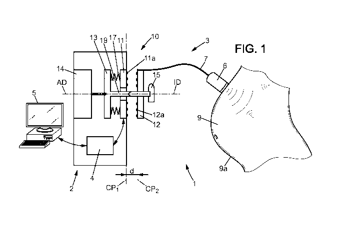
The figure 1 is a schematic view showing an
ultrasound system 1 comprising an electronic device 2 and a
probe 3 that are connected one to the other by a connection
system 10 corresponding to a first embodiment of the
invention. The ultrasound system 1 may be an imaging
ultrasound system that builds an image of a medium on the
basis of received ultrasound waves, or a treatment
ultrasound system that modifies the medium at least at a
predetermined focal point inside the medium, or both or
them doing imaging and treatment. It is understood that the
treatment can be applied to non organic or organic
material. In case of organic material, it could be applied
to in vitro applications or to in vivo application.
The electronic device 2 sends excitation signals to
the probe 3 via the connection system 10 so as to emit at
least an ultrasound wave into a medium 9. The scattering of
the wave inside the medium generates backwards reflected
ultrasound waves that are sensed by the probe 3 and
returned in the form of reflection signals to the
CA 02898692 2015-07-20
WO 2014/128519 PCT/1B2013/000421
7
electronic device 2 via the connection system 10. Such
method applies to ultrasound imaging of the medium as it is
well known. The following description will mainly explained
in view of imaging application. However, it may be also
applied to the treatment application.
The electronic device 2 comprises:
- a first element 11 belonging to the connection
system 10 for sending to the probe 3 said excitation
signals and for receiving from the probe 3 the reflection
signals,
- a processing unit 4 to control said probe 3, for
example for controlling the excitation signals and for
processing the received signals to compute an image
representing the medium 9, and
- a screen 5 to visualize the image to a user.
The probe 3 comprises:
- a second element 12 belonging to the connection
system 10, said second element 12 being adapted to
cooperate with the first element 11 to electrically connect
the probe 3 to the electronic device 2,
- a head 6 comprising a plurality of transducer
elements, e.g. piezoelectric elements, each of them
transforming the electrical signals (excitation and
reflection signals) into an ultrasound wave or inversely,
and
- a cable 7 that links the connection system 10 to
the head 6.
The cable 7 is flexible. A user can move the head 6
above an external surface 9a of the medium 9 to get a
plurality of images from the ultrasound system, each of
said images representing a slice of the inner densities of
the medium 9 at the plurality of positions of the head 6
above the external surface 9a.
Therefore, the connection system 10 comprises at
least:
- a first element 11 having first electrical
CA 02898692 2015-07-20
WO 2014/128519 PCT/1B2013/000421
8
contacts 11a, said first element 11 being attached to the
electronic device 2, and
- a second element 12 having second electrical
contacts 12a for providing an electrical connection between
the first electrical contacts 11a and the second electrical
contacts 12a, said second element 12 being attached to the
probe 3.
When the first and second electrical contacts 11a,
12a are into contact to each other, the first and second
electrical contacts transmit electrical signals from the
probe 3 to the electronic device 2 and from the electronic
device 2 to the probe 3.
The connection system 10 further comprises:
- an actuation device 14, and
- a third element 13.
The actuation device 14 may be any type of actuator
that is able to move the third element 13 relative to the
first element 11 between an activated position and an
inactivated position. The actuation device 14 may be an
electric linear actuator, an electric rotation actuator, an
electric motor, an electric step motor, an electromagnet.
The third element 13 may be suspended relative to
the electronic device 2 or first element 11 by an elastic
element 17, e.g. a coil spring. The position of the third
element 13 without actuation device action can be
predetermined.
The actuation device 14 and the third element 13
are preferably integrated inside the electronic device 2 as
disclosed in the herein presented embodiments. The
electronic device 2 directly controls and powers the
actuation device 14, and the second element 12 (probe
connector) is compact in size and light.
The second
element 12 belonging to the probe 3 is therefore not
modified compared to the known elements of already
available probes. The connection device 10 according to the
herein disclosed embodiments allows backward compatibility:
CA 02898692 2015-07-20
WO 2014/128519 PCT/1B2013/000421
9
Existing probes 3 can be used on an electronic device 2
incorporating said connection systems 10.
The actuation device 14 may be alternatively
integrated inside the probe 3.
The second element 12 is linked to the third
element 13 as explained in the following description.
In the activated position of the third element 13,
the first element 11 is proximal to the second element 12
so as the first electrical contacts 11a can contact the
second electrical contacts 12a to established electric
continuity.
In the inactivated position of the third
element 13, the first element 11 is distant from the second
element 12 so as first electrical contacts 11a can not
contact the second electrical contacts 12a. For example,
the first electrical contacts 11a are at a distance from
the second electrical contacts 12a that is higher than
0.5 mm. The above distance is for example a distance
between a first contacts plane CP' defined by the first
electrical contacts 11a and a second contact plane CP2
defined by the second electrical contacts 12a, in said
inactivated position of the third element 13.
The second element 12 can be removably fixed or
locked to the third element 13 by a locking mechanism 15 to
mechanically connect, plug, or lock the probe 3 to the
electronic device 2. The second element 12 is then in a
locked state.
The second element 12 can be released from the
third element 13 by the same locking mechanism 15 to
mechanically disconnect, unplug or release the probe 3 from
the electronic device 2. The second element 12 is then in a
released state.
The third element 13 is an element that is
intermediate between the first and second elements 11, 12
of the connection system 10. Thanks to this third
element 13, the second element 12 from the probe can be
CA 02898692 2015-07-20
WO 2014/128519 PCT/1B2013/000421
mechanically locked on this third element 13 by the locking
mechanism 15. Thanks to the actuation device 14, the third
element 13 can be moved relative to the first element 11
for electrically connecting or not the second element 12 to
5 the first element 11.
Contrary to prior art connection systems, the
connection system 10 of present invention can provide an
electrical connection of the probe 3 that is independent
from the mechanical locking of the probe 3 to the
10 electronic device 2.
As soon as the probe 3 is removed from the
electronic device 2, after being mechanically disconnected
from it, the probe 3 is also electrically disconnected from
the electronic device 2: The first and second electrical
contacts 11a, 12a do not contact each other and the
electrical continuity is broken between the electronic
device 2 and the probe 3.
The third element 13 of the connection system 10
can be moved by the activation device 14 from the activated
position to the inactivated position, or from the
inactivated position to the activated position, the second
element 12 of the connection system 10 being in any state:
the locked state or the released state, i.e. the second
element 12 being locked to the third element 13 or being
released from the third element 13.
Therefore, the connection system 10 can be in any
of the four following working states Si, S2, S3, S4, that
correspond to all the possibilities of the third element 13
positions and the second element 12 states.
The second element 12 is switched between the
released state and the locked state by the locking
mechanism 15. The third element 13 is switched between the
inactivated position and the activated position by the
activation device 14.
CA 02898692 2015-07-20
WO 2014/128519 PCT/1B2013/000421
11
Third element
(13)
positions
Inactivated Activated
position position
Second element Released 51 S3
(12) states Locked S2 S4
Table 1: all the working states of the connection
system according to the invention
In the working state 51, the third element 13 is in
the inactivated position. The first and second electrical
contacts 11a, 12a are not electrically connected to each
other. The second element 12 is in the released state. The
second element 12 can be removed from the third element 13.
The probe 3 can be mechanically removed from the electronic
device 2. The locking mechanism 15 may be activated by a
user to switch from the working state 51 to the working
state S2, to lock a probe 3 on the electronic device 2.
Additionally, if no probe is present, the processing unit 4
may switch the third element 13 from the inactivated
position (working state 51) to the activated position
(working state S3). In that case, the third element 13 is
moved by the activation device 14 without any probe.
In the working state S2, the second element 12 is
now locked on the third element 13, and the probe 3 is
locked on the electronic device 2 and can not be directly
removed from the third element 13. The locking mechanism 15
must be activated by a user to switch back to the working
state 51 and to release the second element 12, i.e.
probe 3. Alternatively, the user may interfere with the
ultrasound imaging system 1 and the electronic device 2
(processing unit 4) may switch the third element 13 from
the inactivated position to the activated position to
switch from the working state S2 to the working state S4.
In the working state S3, the third element 13 is in
CA 02898692 2015-07-20
WO 2014/128519 PCT/1B2013/000421
12
the activated position. The second element 12 is in the
released state, and can be removed from the third
element 13. The probe 3 can be mechanically removed from
the electronic device 2. The locking mechanism 15 may be
activated by a user to switch from the working state S3 to
the working state S4 to lock the probe 3 on the electronic
device 2. Such working state S3 is therefore a state that
should be transient, and that should not be a normal use
state.
In the working state S4, the second element 12 is
locked on the third element 12, and the probe 3 is also
locked on the electronic device 2. The locking mechanism 15
must be activated by a user to switch back to the working
state S3 (unlocking or releasing of the probe). The
processing unit 4 may switch the third element 13 from the
activated position to the inactivated position to switch
from the working state S4 to the working state S2.
The switch between the working states S2 and S4
correspond to the activation of connection system 10. This
electrically connects or not the first electrical
contacts 11a with the second electrical contacts 12a. The
processing unit 4 can switch the third element 13 from the
inactivated position (working state S2) to the activated
position (working state S4). In that case, the third
element 13 is moved by the activation device 14, the second
element 12 of the probe 3 being installed inside the
connection system 10. The actuation device 14 is therefore
moving (controlling) the first and second electrical
contacts 11A, 12a so as they are switch to electrical
contacts or not. They are functioning like electrical
switches that are usually used for connecting only one
particular selected probe in an electronic device 2 having
a plurality of probes connected on it.
Thanks to the above four working states, the second
element 12 can be locked or released from the third
element 13 independently from the position of the third
CA 02898692 2015-07-20
WO 2014/128519 PCT/1B2013/000421
13
element 13 relative to the first element 11: in the
activated or inactivated position. The probe 3 connected to
the connection system 10 can be removed from the ultrasound
electronic device 2 rapidly by a user.
The activation device 14 is preferably moving the
third element 13 according to an activation direction AD
that is perpendicular to the first contact plane CP'. The
first and second contact planes CPI, CP2 are preferably
parallel to each other.
The second element 12 is for example locked or
released to the third element 13 according to an insertion
direction ID, said insertion direction being not parallel
to the first contact plane CPI, and being preferably
perpendicular to said first contact plane CP'. The second
element 12 is therefore locked or released to the third
element according to a direction that is the same as the
activation direction AD that moves the third element 13
relative to the first element 11.
The connection system may have the following
features: The third element 13 is situated inside the
electronic device bellow the first element 11 so as it is
directly moved and controlled by the actuation device 14
inside the electronic device 2. The first element 11 is
situated at an external surface of a casing of the
electronic device so as to cooperate with the second
element 12 from the probe 3. The first element 11 comprises
a hole, and the third element 13 comprise a connecting
shaft 19 extending at least partially through said hole to
the outside of the electronic device 2. The connecting
shaft 19 can therefore cooperate with the locking
mechanism 15 of the probe 3 so as to lock or unlock the
second element 12 to the third element 13: The second
element 12 is at positioned at a predetermined position
relative to the third element 13. The shaft extends
according to the insertion direction ID through the hole of
the first element 11.
CA 02898692 2015-07-20
WO 2014/128519 PCT/1B2013/000421
14
The locking mechanism 15 is capable to fix or lock
the second element 12 at said predetermined position
(locked state) or to release the second element 12 so as it
can be removed from the electronic device 2. The locking
mechanism comprises (at a first end in the direction of the
electronic device) a nose adapted to cooperate with the
connecting shaft 19 for locking or releasing said second
element 12.
The locking mechanism 15 may be of any kind. For
example, it is a rotatable handle mounted on the second
element 12, said handle being rotated by a user to lock or
release the second element from the third element 13. The
probe 3 can therefore be extracted from the electronic
device 2 at any time: The third element 13 being in an
activated or inactivated position, and the electronic
device 2 being powered or not.
The electronic device 2 may advantageously comprise
a plurality of first elements 11 for connecting a plurality
of probes. Usually, such electronic device 2 comprises
inner electrical switches to select simultaneously only one
probe. The patent US 4 726 230 discloses an example of such
electronic device.
The actuation device 14 in present invention
replaces the electrical switches included inside the above
prior art imaging system. In case of a connection system
having lots of electrical contacts (for probes having lots
of transducers elements), this is really advantageous: For
example, in case of a probe head 6 having a number of
500 transducers elements, such prior art electronic device
must incorporate the same number of electrical switches for
each one connection system, i.e. for each probe slot
(receptacle) of the electronic device. Such architecture
leads to an enormous number of electrical switches that use
electronic board area and that are costly.
By using the connection system 10 as a switch for
CA 02898692 2015-07-20
WO 2014/128519 PCT/1B2013/000421
all the electrical contacts or wires from a probe, the need
for all these switches is eliminated. The document
US 5 882 310 discloses an electronic device that comprises
such controlled connection system, but this system permits
5 to electrically connect simultaneously only one probe to
the electronic device 2. When electrically connected, such
connection system is also mechanically locked, and the
probe can not be easily unplugged from the electronic
device. Such connection system can only work in the above
10 defined working states Si and 54, and can not work in the
working states S2 and 53.
The connection system 10 according to the invention
therefore differs in that the electrical connection of the
probe 3 to the electronic device 2 is independent from the
15 mechanical locking of the probe 3 to said electronic
device 2.
The actuation device 14 of present invention may
use some space inside the electronic device 2, but an
electronic device 2 incorporating said connection system 10
can have a reduced size. And, it is also less costly.
Figure 2 shows a first example of an electronic
device 2 used in conjunction with a plurality of connection
systems 10. In the figure, the
electronic device 2
comprises four first elements. The first elements 11 are
individually denoted with the reference numbers 111, 112,
113, and 114.
A first probe 31 comprises a second element 121 and
is ready to be connected to the first element 111. A second
probe 32 comprising a second element 122 is already
connected to the first element 114. The first elements 112
and 113 are not presently used. The user mechanically plugs
or unplugs each of the probes 31, 32 to the electronic
device 2 by their locking mechanisms 15.
As illustrated in figure 3, the electronic device 2
comprises a processing unit 4 and first elements 111
to 114. All the first electrical contacts of the first
CA 02898692 2015-07-20
WO 2014/128519 PCT/1B2013/000421
16
elements are connected to the processing unit 4 via a
signal bus 6 comprising for example a number of lines equal
to the number of first electrical contacts of one of the
first elements. The signal bus 6 comprises a plurality of
branches (61, 62, 63, 64), one branch for connecting one of
the first elements (111, 112, 113, 114). An electrical
contact of a first element 11 is therefore connected to an
equivalent electrical contact of another first element 11.
Figure 4 shows a second example of an electronic
device 2 used in conjunction with a plurality of connection
systems 10.
The electronic device 2 comprises first elements
organized according to a matrix arrangement, having rows
and columns. The electronic device 2 also comprises a
number of signal buses corresponding to the number of rows
to interconnect the first elements belonging to said row.
Thanks to the above feature, a plurality of probes
may be connected simultaneously, one on each row. The
number of transducer elements can therefore be increased.
By using two probes having for example 128 transducers
elements, the imaging system can behave such as having a
unique 256 transducer elements. Different probes can be
also connected simultaneously: probes having different
transducer elements arrangements (linear, curved, matrix),
or probes for different use (a probe for imaging the
medium, or a probe for medium treatment). Each signal bus
may comprise electronic interface adapted to the use of the
probes that can be connected to it (imaging or treatment).
The electronic interface for example comprises amplifies,
multiplexers, analog to digital converters, digital to
analog converters, etc_ as it is well known.
For example, the electronic device of figure 4
comprises two rows and four columns. The first row
comprises a fist signal bus 6a to interconnect the first
elements, denoted with the reference numbers 11a1, 11a2,
11a3, and 11a4, via fist branches of said first bus 6a.
CA 02898692 2015-07-20
WO 2014/128519 PCT/1B2013/000421
17
Similarly, the second row comprises a second signal bus 6b
to interconnect the first elements denoted with the
reference numbers 11b1, 11b2, 11b3, and 11b4 via second
branches of said second bus 6b. The first and second signal
buses 6a, 6b
are linked to the processing unit 4
separately.
According to a first variant, all the first
elements 11 of the matrix arrangement may be independent
from the other. Each first element 11 is for example
embedded inside a connection unit comprising said first
element 11, a single activation device 14, and a single
third element 13 actuated by said activation device 14.
According to a second variant, the first
elements 11 of a column (of index i) may be grouped into a
connection unit that comprises the first elements llai,
llbi, a single activation device 14, and a single third
element 13 actuated by said activation device 14. However
one or two distinct probes can be connected to the single
third element 13 of said connection unit. The probes are
therefore independently mechanically plugged or unplugged
to the connection unit (electronic device 2), but the
single actuation device 14 electrically connect or the
probes by moving said single third element 13 between the
inactivated position and the activated position.
Such electronic device 2 can provide numerous
configurations. For example, a first probe can be plugged
to the first row of a column, and a second probe can be
plugged to the second row of another column. In that case,
both probes are independently controlled.
Figures 5 and 6 are representing a first embodiment
of the connection system 10 wherein the electronic device 2
comprises connection unit incorporating a first element 11,
a third element 13 and an activation device 14. The
activation device 14 is a linear motor actuating a shaft
according to the activation direction AD. The activation
CA 02898692 2015-07-20
WO 2014/128519 PCT/1B2013/000421
18
device 14 is also mounted on a mounting plate 20 fixed
inside the electronic device 2. The shaft can move the
third element 13 according said acttivation direction AD.
The probe 3 comprises a locking mechanism 15 in the
form of a manual handle that is rotatable according to the
insertion direction ID, said insertion direction being
parallel to the activation direction AD. The locking
mechanism comprises a locking shaft 16 adapted to be locked
to the third element 13, via the connecting shaft 19.
Figure 7 represents a second embodiment of the
connection system 10 wherein the actuation device 14 is a
rotation motor. Said rotation motor rotates a wheel 21
having an eccentric pin. The eccentric pin is engaged
inside an elongated hole of a support 23 fixed to the
mounting plate 20. The rotation movement of the actuation
device 14 is transformed into a linear displacement of the
third element 13.