Note : Les descriptions sont présentées dans la langue officielle dans laquelle elles ont été soumises.
1
SEMICONDUCTOR AMPLIFIER BIAS CIRCUIT AND
SEMICONDUCTOR AMPLIFIER DEVICE
FIELD
Embodiments described herein relate generally a
semiconductor amplifier bias circuit and a semiconductor amplifier
device.
BACKGROUND
In a microwave semiconductor amplifying element, high
efficiency operation can be achieved when the load impedance for
the second harmonic seen from the output electrode end of the
semiconductor amplifying element is made near-open.
In this case, it is assumed that the load impedance for the
second harmonic signal seen from the output end part of the package
is e.g. approximately 50 Q or more. Here, the term "approximately
50 Q" means 47 Q or more and 53 Q or less.
However, when a bias circuit is provided between the output
matching circuit and the external load, the load impedance for almost
part of the second harmonic signal seen from the output end part of
the package may fall below 50 Q. This may decrease the efficiency.
SUMMARY OF THE INVENTION
According to an aspect of the present invention there is
provided a semiconductor amplifier bias circuit provided between an
output matching circuit of a semiconductor amplifying element and
an external load comprising:
a first transmission line connected to an output end part of the
output matching circuit and the external load;
CA 2900000 2017-07-05
la
a first grounded shunt capacitor;
a second transmission line including one end part connected to
the first transmission line and the other end part connected to the
first grounded shunt capacitor, electrical length of the second
transmission line being 81 or more and 99 or less at a center
frequency of a band, the one end part being connected to the first
transmission line at a position apart from the output end part by an
electrical length of 40.5 or more and 49.50 or less at the center
frequency; and
a power supply terminal connected to a connection point of the
first grounded shunt capacitor and the other end part of the second
transmission line,
load impedance being equal to a resistance of the external load
for fundamental signal, as viewed from a connection point between
the first transmission line and the output matching circuit, and
load impedance being open for second harmonic signal, as
viewed from the connection point between the first transmission line
and the output matching circuit.
According to another aspect of the present invention there is
provided a semiconductor amplifier device comprising:
the semiconductor amplifier bias circuit as described herein;
a semiconductor amplifying element; and
an output matching circuit including a bonding wire connected
to the semiconductor amplifying element and a transmission line
connected to the bonding wire, an electrical length of the
transmission line at an upper limit frequency of the band being 900
or less at an upper limit frequency of the band,
load impedance seen from an output electrode of the
semiconductor amplifying element being open for the second
harmonic signal.
CA 2900000 2017-07-05
CA 02900000 2017-01-12
lb
BRIEF DESCRIPTION OF THE DRAWINGS
FIG. 1A is a circuit diagram of a semiconductor amplifier device
according to a first embodiment, and FIG. 1B is a circuit diagram of
a feed branch section of an external bias circuit;
FIG. 2A is a Smith chart showing the load impedance seen from
the reference plane QO in the feed branch section of
CA 02900000 2015-08-10
2
the semiconductor amplifier device of the first embodiment, FIG.
2B is a Smith chart showing the load impedance seen from the
reference plane Q, FIG. 2C is a Smith chart showing the load
impedance seen from the reference plane Q2, FIG. 2D is a
Smith chart showing the load impedance seen from the
reference plane Q3, and FIG. 2E is a Smith chart showing the
load impedance seen from the reference plane Q4;
FIG. 3A is a circuit diagram of the semiconductor
amplifier of the first embodiment in which no output bias circuit
is connected, FIG. 3B is a Smith chart showing the load
impedance seen from the reference plane Q2 in the
semiconductor amplifier device of the first embodiment, FIG. 3C
is a Smith chart showing the load impedance seen from the
reference plane Q3, and FIG. 3D is a Smith chart showing the
load impedance seen from the reference plane Q4;
FIG. 4A is a configuration diagram of a semiconductor
amplifier device according to a comparative example, and FIG.
4B is a circuit diagram of a feed branch section of an external
bias circuit;
FIG. 5A is a Smith chart showing the load impedance
seen from the reference plane QO in the feed branch section of
the semiconductor amplifier device of the comparative example,
FIG. 5B is a Smith chart showing the load impedance seen from
the reference plane Ql, FIG. 5C is a Smith chart showing the
load impedance seen from the reference plane Q2, FIG. 5D is a
Smith chart showing the load impedance seen from the
reference plane Q3, and FIG. 5E is a Smith chart showing the
load impedance seen from the reference plane Q4;
FIG. 6A is a circuit diagram of a semiconductor amplifier
device according to a second embodiment, and FIG. 6B is a
circuit diagram of a feed branch section of an external bias
circuit;
FIG. 7A is a Smith chart showing the load impedance
seen from the reference plane QO in the feed branch section of
the semiconductor amplifier device of the second embodiment,
FIG. 7B is a Smith chart showing the load impedance seen from
CA 02900000 2015-08-10
3
the reference plane Ql, FIG. 7C is a Smith chart showing the
load impedance seen from the reference plane Q2, FIG. 7D is a
Smith chart showing the load impedance seen from the
reference plane Q3, and FIG. 7E is a Smith chart showing the
load impedance seen from the reference plane Q4;
FIG. 8A is a circuit diagram of a semiconductor amplifier
device according to a third embodiment, and FIG. 8B is a circuit
diagram of a feed branch section of an external bias circuit;
FIG. 9A is a Smith chart showing the load impedance
seen from the reference plane QO in the feed branch section of
the semiconductor amplifier device of the third embodiment,
FIG. 9B is a Smith chart showing the load impedance seen from
the reference plane Ql, FIG. 9C is a Smith chart showing the
load impedance seen from the reference plane Q2, FIG. 9D is a
Smith chart showing the load impedance seen from the
reference plane Q3, and FIG. 9E is a Smith chart showing the
load impedance seen from the reference plane Q4;
FIG. 10A is a Smith chart showing the load impedance
seen from the reference plane QO in the feed branch section of
the semiconductor amplifier device (X=45 ) of the third
embodiment, FIG. 10B is a Smith chart showing the load
impedance seen from the reference plane Q1, FIG. 10C is a
Smith chart showing the load impedance seen from the
reference plane Q2, FIG. 10D is a Smith chart showing the load
impedance seen from the reference plane Q3, and FIG. 10E is a
Smith chart showing the load impedance seen from the
reference plane Q4;
FIG. 11A is a circuit diagram of a semiconductor amplifier
device according to a fourth embodiment, and FIG. 11B is a
circuit diagram of a feed branch section of an external bias
circuit;
FIG. 12A is a Smith chart showing the load impedance
seen from the reference plane QO in the feed branch section of
the semiconductor amplifier device of the fourth embodiment,
FIG. 12B is a Smith chart showing the load impedance seen
from the reference plane Ql, FIG. 12C is a Smith chart showing
CA 02900000 2015-08-10
4
the load impedance seen from the reference plane Q2, FIG. 12D
is a Smith chart showing the load impedance seen from the
reference plane Q3, and FIG. 12E is a Smith chart showing the
load impedance seen from the reference plane Q4;
FIG. 13A is a circuit diagram of a semiconductor amplifier
device according to a fifth embodiment, and FIG. 13B is a
circuit diagram of a feed branch section of an external bias
circuit; and
FIG. 14A is a Smith chart showing the load impedance
seen from the reference plane QO in the feed branch section of
the semiconductor amplifier device of the fifth embodiment, FIG.
14B is a Smith chart showing the load impedance seen from the
reference plane Q1, FIG. 14C is a Smith chart showing the load
impedance seen from the reference plane Q2, FIG. 14D is a
Smith chart showing the load impedance seen from the
reference plane Q3, and FIG. 14E is a Smith chart showing the
load impedance seen from the reference plane Q4.
DETAILED DESCRIPTION
In general, according to one embodiment, a
semiconductor amplifier bias circuit includes a first transmission
line, a first grounded capacitor, a second transmission line and a
power supply terminal. The first transmission line is connected
to an output end part of the output matching circuit and the
external load. The second transmission line includes one end
part connected to the first transmission line and the other end
part connected to the first grounded shunt capacitor. An
electrical length of the second transmission line is
approximately 900 at a center frequency of a band. The one
end part is connected to the first transmission line at a position
apart from the output end part by an electrical length of
approximately 450 at the center frequency. The power supply
terminal is connected to a connection point of the first grounded
shunt capacitor and the other end part of the second
transmission line.
Embodiments of the invention will now be described with
CA 02900000 2015-08-10
reference to the drawings.
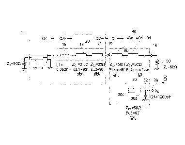
FIG. 1A is a circuit diagram of a semiconductor amplifier
device according to a first embodiment. FIG. 1B is a circuit
diagram of a feed branch section of an external bias circuit.
5 The semiconductor amplifier device includes a packaged
semiconductor amplifier 11 and a (semiconductor amplifier) bias
circuit 34.
The packaged semiconductor amplifier 11 includes a
semiconductor amplifying element 14, an input matching circuit
12, and an output matching circuit 20. The bias circuit 34
shown in FIGS. 1A and 1B is connected between the output end
part 19 of the package and an external load 50.
The bias circuit 34 is connected between the packaged
semiconductor amplifier 11 and the external load 50. In this
case, the characteristic impedance Zczi of the first transmission
line 40 of the bias circuit 34 is made equal to the resistance ZL
of the external load 50. Then, impedance matching between
the first transmission line 40 and the external load 50 is easily
achieved. Thus, the load impedance for the fundamental signal
seen from the reference plane Q2 (i.e., output end part 19) is
equal to the resistance ZL. The resistance ZL can be set to e.g.
50Q.
The semiconductor amplifying element 14 includes e.g. a
HEMT (high electron mobility transistor) or GaAs MESFET (metal
semiconductor field effect transistor). The
semiconductor
amplifying element 14 has an amplification function in the
microwave band.
The output matching circuit 20 includes a bonding wire
15 and a transmission line 16. The bonding wire 15 is
connected to the semiconductor amplifying element 14. The
transmission line 16 is connected to the bonding wire 15. The
electrical length EL1 of the transmission line 16 is 90 or less at
the upper limit frequency fH of the band. As shown in FIGS. 1A
and 1B, the output matching circuit 20 may further include a
transmission line 21. The transmission line 21 is cascaded to
the transmission line 16. The
electrical length EL2 of the
CA 02900000 2015-08-10
6
transmission line 21 is 900 or less at the center frequency fc of
the band.
The bias circuit 34 includes a first transmission line 40, a
first grounded shunt capacitor 32, a second transmission line 30,
and a power supply terminal 39. The first transmission line 40
is a main signal line. The second transmission line 30 is
branched from the first transmission line 40. The first
transmission line 40 includes one end part connected to the
output end part 19 of the output matching circuit 20, and the
other end part (being an output terminal of the amplifier
device) connected to the external load 50.
The electrical length EL3 of the second transmission line
30 is approximately 90 at the center frequency fc of the band.
One end part of the second transmission line 30 is connected to
the first transmission line 40 at the position apart from the
output end part 19 by an electrical length EL4 of approximately
45 . The other end part of the second transmission line 30 is
connected to the power supply terminal 39 and the first
grounded shunt capacitor 32.
In this specification, the statement that the electrical
length of a transmission line is approximately 90 means that
the electrical length is 81 or more and 99 or less. The
statement that the electrical length of a transmission line is
approximately 450 means that the electrical length is 40.5 or
more and 49.5 or less.
The output matching circuit 20 is designed so that, for
instance, the load impedance for the second harmonic signal
seen from the output end part 19 of the package is also 50
for all frequencies including the fundamental and the second
harmonic. The bias circuit is provided between the output end
part 19 and the external load 50. In this
case, the load
impedance for almost part of the second harmonic signal seen
from the output end part 19 may fall below 50 Q due to the
influence of the bias circuit.
First, the load impedance in the case of no output bias
circuit is described for comparison purposes.
CA 02900000 2015-08-10
7
FIG. 3A is a circuit diagram of the semiconductor
amplifier of the first embodiment in which no output bias circuit
is connected. FIG. 3B is a
Smith chart showing the load
impedance seen from the reference plane Q2 (output end part
of the package) in the semiconductor amplifier of the first
embodiment. FIG. 3C is a
Smith chart showing the load
impedance seen from the reference plane Q3 (wire end). FIG.
3D is a Smith chart showing the load impedance seen from the
reference plane Q4 (semiconductor element end).
As shown in FIG. 3A, in the first embodiment, for
instance, a bonding wire 15, a transmission line 16, and a
transmission line 21 are series connected in the output
matching circuit 20. The
transmission line 16 has a
characteristic impedance Zci of 3.5 Q and an electrical length
EL1 of 900 or less (at fH). The transmission line 21 has a
characteristic impedance ZC2 of 20 SI and an electrical length
EL2 of 900 or less (at fc). The characteristic impedance Zcz of
the transmission line 21 is normally made lower than 50 0.
The characteristic impedance Zci of the transmission line
16 is set between the characteristic impedance ZC2 of the
transmission line 21 and the resistance component of the
output impedance of the semiconductor amplifying element 14.
In this case, impedance transformation is performed by the
transmission lines 21, 16 and the wire 15. Thus, the load
impedance for the fundamental signal seen from the
semiconductor element end can be made close to the output
impedance desired for the semiconductor amplifying element
14.
As shown in FIG. 3B, when the load impedances for the
fundamental and second harmonic signals seen from the
reference plane Q2 (package end) are both 50 f2, the electrical
length EL1 of the transmission line 16 is set to 90 or less (at
fH). Thus, as shown in FIG. 3C, the load impedance m5 for the
second harmonic signal (at 2fc) as viewed from the reference
plane Q3 (wire end) is made near-open impedance and
inductive.
CA 02900000 2015-08-10
8
Furthermore, the inductance of the wire is added. Then,
as shown in FIG. 3D, the output matching circuit 20 can be
designed so that the load impedance for the second harmonic
signal seen from the reference plane Q4 (semiconductor
amplifying element end) is transformed to a further near-open
impedance while matching the fundamental signal.
Next, the load impedance including the influence of the
output bias circuit is described.
FIG. 2A is a Smith chart showing the load impedance
seen from the reference plane QO in the feed branch section of
the semiconductor amplifier device of the first embodiment.
FIG. 2B is a Smith chart showing the load impedance seen from
the reference plane Q1 (feed branch connection point). FIG.
2C is a Smith chart showing the load impedance seen from the
reference plane Q2 (output end part of the package). FIG. 2D
is a Smith chart showing the load impedance seen from the
reference plane Q3 (wire end). FIG. 2E is a
Smith chart
showing the load impedance seen from the reference plane Q4
(semiconductor element end).
The impedance can be estimated by circuit simulation.
The resistance ZL of the external load 50 is set to ZL = 50 Q.
The characteristic impedance Zc4 of the first transmission line
40 is set to ZC4 = 50 Q. The characteristic impedance Zc3 of
the second transmission line 30 is set to ZC3 = 50 n. The
connection position 80 of one end part of the second
transmission line 30 and the first transmission line 40 is located
at an electrical length EL4a of approximately 45 from the
output end part 19 of the output matching circuit 20 toward the
external load 50. Here, the electrical length EL4b may be an
arbitrary length.
The electrical length EL3 of the second transmission line
30 is set to approximately 90 at the fundamental signal (fc).
The capacitance Cl of the first grounded shunt capacitor 32 is
set to 1000 pF or more. Then, the second transmission line 30
is tip-short at the center frequency fc (e.g., 3 GHz). The power
supply terminal 39 is supplied with a DC voltage VD (drain
CA 02900000 2015-08-10
9
voltage in the case of HEMT).
As shown in FIG. 2A, as viewed from the reference plane
QO in the feed branch section of the semiconductor amplifier
device of the first embodiment, the load impedance for the
fundamental signal is near-open, and the load impedance for
the second harmonic signal is near-short.
This feed branch is connected to the first transmission
line 40. Then, as shown in FIG. 2B, as viewed from the
reference plane Q1 (feed branch connection point) in the
semiconductor amplifier device of the first embodiment, the
load impedance for the fundamental signal is approximately 50
Q, and the load impedance for the second harmonic signal is
near-short.
The electrical length EL4a of the first transmission line 40
is approximately 450. Thus, as shown in FIG. 2C, as viewed
from the reference plane Q2 (output end part 19 of the
package) in the semiconductor amplifier device of the first
embodiment, the load impedance for the fundamental signal is
approximately 50 Q, and the load impedance for the second
harmonic signal is near-open.
As viewed from the output end part of the package, the
load impedance for the fundamental signal is approximately 50
Q, and the load impedance for the second harmonic signal is
approximately 50 Q or more. Thus, as shown in FIG. 2D, the
load impedance for the second harmonic signal seen from the
reference plane Q3 (wire end) is made near-open impedance
and inductive.
Furthermore, the inductance of the wire is added. Then,
as shown in FIG. 2E, the load impedance for the second
harmonic signal seen from the reference plane Q4
(semiconductor end) can be transformed to a further near-open
impedance while matching the fundamental signal.
Thus, the load impedance for the second harmonic signal
seen from the output end part 19 of the package is set to
approximately 50 Q or more by configuring the output bias
circuit 34 as described above. As a result, the load impedance
CA 02900000 2015-08-10
for the second harmonic signal seen from the reference plane
Q4 (semiconductor amplifying element end) is made near-open
impedance. Thus, the efficiency is improved.
FIG. 4A is a configuration diagram of a semiconductor
5 amplifier device according to a comparative example. FIG. 4B
is a circuit diagram of a feed branch section of an external bias
circuit.
The semiconductor amplifier device includes a packaged
semiconductor amplifier 111 and a bias circuit 134. The
10 packaged semiconductor amplifier 111 includes a semiconductor
amplifying element 114, an input matching circuit 112, and an
output matching circuit 120. The bias circuit 134 is connected
between the output end part 119 of the package and an
external load 150. The only difference from the first
embodiment shown in FIGS. 1A and 1B is that there is no
transmission line having an electrical length of approximately
450 between the connection point 180 connected with the feed
branch and the output end part 119 of the package.
FIG. 5A is a Smith chart showing the load impedance
seen from the reference plane QO in the feed branch section of
the semiconductor amplifier device of the comparative example.
FIG. 5B is a Smith chart showing the load impedance seen from
the reference plane Q1 (feed branch connection point). FIG.
5C is a Smith chart showing the load impedance seen from the
reference plane Q2. FIG. 5D is a Smith chart showing the load
impedance seen from the reference plane Q3. FIG. 5E is a
Smith chart showing the load impedance seen from the
reference plane Q4 (semiconductor element end).
As shown in FIG. 5A, as viewed from the reference plane
QO in the feed branch section of the semiconductor amplifier
device of the comparative example, the load impedance for the
fundamental signal is near-open, and the load impedance for
the second harmonic signal is near-short.
This feed branch is connected. Then, as shown in FIG.
5B, as viewed from the reference plane Q1 (feed branch
connection point) in the semiconductor amplifier device of the
CA 02900000 2015-08-10
11
comparative example, the load impedance for the fundamental
signal is approximately 50 0, and the load impedance for the
second harmonic signal is near-short.
There is no transmission line between the connection
point 180 connected with the feed branch and the output end
part 119 of the package. Thus, as shown in FIG. 5C, the load
impedance seen from the reference plane Q2 (output end part
of the package) in the semiconductor amplifier device of the
comparative example is equal to the load impedance seen from
the reference plane Q1 (feed branch connection point). The
load impedance for the fundamental signal is approximately 50
S2, and the load impedance for the second harmonic signal is
near-short.
As viewed from the output end part 119 of the package,
the load impedance for the fundamental signal is 50 0, but the
load impedance for the second harmonic signal is near-short.
Thus, as shown in FIG. 5D, the load impedance for the second
harmonic signal seen from the reference plane Q3 (wire end)
exhibits a large frequency dependence.
Furthermore, even if the inductance of the wire is added,
as shown in FIG. 5E, the load impedance for the second
harmonic signal seen from the reference plane Q4
(semiconductor amplifying element end) cannot be transformed
to near-open impedance, although the fundamental signal is
matched.
Thus, the load impedance for the second harmonic signal
seen from the output end part 119 of the package is set to 50 0
or less by configuring the output bias circuit 134 as described
above. As a result,
the load impedance for the second
harmonic signal seen from the reference plane Q4
(semiconductor amplifying element end) cannot be made
near-open impedance. Thus, the efficiency is not improved.
In contrast, in the semiconductor amplifier device
according to the first embodiment and the bias circuit 34
constituting the semiconductor amplifier device, the second
harmonic signal impedance can be maintained at near-open
CA 02900000 2015-08-10
12
impedance while maintaining the fundamental signal matching.
This enables high efficiency operation.
FIG. 6A is a circuit diagram of a semiconductor amplifier
device according to a second embodiment. FIG. 6B is a circuit
diagram of a feed branch section of an external bias circuit.
The bias circuit 34 can further include an inductor 60 and
a grounded shunt capacitor 33 between the other end part of
the second transmission line 30 grounded for radio frequency
and the power supply terminal 39. The grounded
shunt
capacitor 33 serves as a good ground for signals in the band.
The inductance L2 of the inductor 60 is set to e.g. 100 nH.
Then, the impedance can be made higher for the second
harmonic signal. Thus, the bias circuit 34 can be made less
susceptible to the influence of the power supply terminal 39.
Except for the bias circuit 34, the configuration is similar to that
of the first embodiment.
FIG. 7A is a Smith chart showing the load impedance
seen from the reference plane QO in the feed branch section of
the semiconductor amplifier device of the second embodiment.
FIG. 7B is a Smith chart showing the load impedance seen from
the reference plane Q1 (feed branch connection point). FIG.
7C is a Smith chart showing the load impedance seen from the
reference plane Q2 (output end part of the package). FIG. 7D
is a Smith chart showing the load impedance seen from the
reference plane Q3 (wire end). FIG. 7E is a
Smith chart
showing the load impedance seen from the reference plane Q4
(semiconductor amplifying element end).
As shown in FIG. 7C, the load impedance for the second
harmonic signal seen from the reference plane Q2 (output end
part 19 of the package) is successfully set to 50 SI or more.
Thus, as shown in FIG. 7E, the load impedance for the second
harmonic signal seen from the reference plane Q4
(semiconductor amplifying element end) is made near-open
impedance while matching the fundamental signal. Thus, the
efficiency is improved.
FIG. 8A is a circuit diagram of a semiconductor amplifier
CA 02900000 2015-08-10
13
device according to a third embodiment. FIG. 86 is a circuit
diagram of a feed branch section of an external bias circuit.
The bias circuit 34 includes a first transmission line 40, a
second transmission line 30, an open stub line 31, and a power
supply terminal 39. The first transmission line 40 includes one
end part connected to the output end part 19 of the output
matching circuit 20, and the other end part connected to the
external load 50. The characteristic impedance ZC4 of the first
transmission line 40 is set to 50 Q. The
characteristic
impedance ZC3 of the second transmission line 30 can be set to
50 O. The electrical length EL3 thereof is set to approximately
90 at the center frequency (fc).
One end part of the second transmission line 30 is
connected to the first transmission line 40. One end part of
the second transmission line 30 is connected to the first
transmission line 40 at a connection position 80 where the
electrical length from the output end part 19 is X . Here,
0`)X180 . The
characteristic impedance ZC4 of the first
transmission line 40 is made equal to the resistance ZL of the
external load 50. Then, the electrical length between the
connection position 80 and the output terminal 18 does not
affect the impedance.
The open stub line 31 includes one end part connected to
the other end part of the second transmission line 30 at a
connection position 82, and the other end part having an
electrical length EL5 of approximately 90 at the center
frequency fc and being tip-open. The characteristic impedance
Zcs of the open stub line 31 is set to e.g. 50 Q. The power
supply terminal 39 is DC connected to the other end part of the
second transmission line 30.
An inductor 60 can be further provided between the other
end part of the second transmission line 30 and the power
supply terminal 39. The
configuration except for the bias
circuit 34 is the same as that of the first embodiment.
The other end part of the second transmission line 30 is
grounded not by a lumped-parameter ground capacitance, but
CA 02900000 2015-08-10
14
by the open stub line 31 having an electrical length EL5 of
approximately 90 at the center frequency fc. Thus, at the
connection position 82 of the open stub line 31, the impedance
for the fundamental signal is near-short impedance. On the
other hand, at the connection position 82 of the open stub line
31, the impedance for the second harmonic signal is made
near-open impedance.
FIG. 9A is a Smith chart showing the load impedance
seen from the reference plane QO in the feed branch section of
the semiconductor amplifier device (X=0 ) of the third
embodiment. FIG. 9B is a
Smith chart showing the load
impedance seen from the reference plane Q1 (feed branch
connection point). FIG. 9C is a Smith chart showing the load
impedance seen from the reference plane Q2 (output end part
of the package). FIG. 9D is a Smith chart showing the load
impedance seen from the reference plane Q3. FIG. 9E is a
Smith chart showing the load impedance seen from the
reference plane Q4.
As shown in FIG. 9A, as viewed from the reference plane
QO in the feed branch section of the semiconductor amplifier
device of the third embodiment, the load impedance for the
fundamental signal is near-open, and the load impedance for
the second harmonic signal is also near-open.
This feed branch is connected. Then, as shown in FIG.
9B, as viewed from the reference plane Q1 (feed branch
connection point) in the semiconductor amplifier device of the
third embodiment, the load impedance for the fundamental
signal is approximately 50 n, and the load impedance for the
second harmonic signal is also approximately 50 Q.
Also when the electrical length X of the first transmission
line 40 is 0 , as shown in FIG. 9C, as viewed from the reference
plane Q2 (output end part 19 of the package) in the
semiconductor amplifier device of the third embodiment, the
load impedance for the fundamental signal is approximately 50
S2, and the load impedance for the second harmonic signal is
approximately 50 O.
CA 02900000 2015-08-10
As viewed from the output end part 19 of the package,
the load impedance for the fundamental signal is approximately
50 0, and the load impedance for the second harmonic signal is
approximately 50 Q. Thus, as shown in FIG. 9D, the load
5 impedance for the second harmonic signal seen from the
reference plane Q3 (wire end) is made near-open impedance
and inductive.
Furthermore, the inductance of the wire is added. Then,
as shown in FIG. 9E, the load impedance for the second
10 harmonic signal seen from the reference plane Q4
(semiconductor amplifying element end) can be transformed to
a further near-open impedance while matching the fundamental
signal.
Thus, also when X=0 , the load impedance for the second
15 harmonic signal seen from the output end part 19 of the
package is set to approximately 50 0 or more by configuring
the output bias circuit 34 using the open stub line 31 as
described above. As a result,
the load impedance for the
second harmonic signal seen from the reference plane Q4
(semiconductor amplifying element end) is made near-open
impedance. Thus, the efficiency is improved.
FIG. 10A is a Smith chart showing the load impedance
seen from the reference plane QO in the feed branch section of
the semiconductor amplifier device (X=45 ) of the third
embodiment. FIG. 10B is a Smith chart showing the load
impedance seen from the reference plane Q1 (feed branch
connection point). FIG. 10C is a Smith chart showing the load
impedance seen from the reference plane Q2 (output end part
of the package). FIG. 10D is a Smith chart showing the load
impedance seen from the reference plane Q3 (wire end). FIG.
10E is a Smith chart showing the load impedance seen from the
reference plane Q4 (semiconductor element end).
As shown in FIG. 10B, as viewed from the reference
plane Q1 (feed branch connection point) in the semiconductor
amplifier device of the third embodiment, the load impedance
for the fundamental signal is approximately 50 0, and the load
CA 02900000 2015-08-10
16
impedance for the second harmonic signal is also approximately
50 Q. Thus, also in the case of X=45 , as shown in FIG. 10C,
as viewed from the reference plane Q2 (output end part 19 of
the package) in the semiconductor amplifier device of the third
embodiment, the load impedance for the fundamental signal is
approximately 50 D, and the load impedance for the second
harmonic signal is approximately 50 0.
As viewed from the output end part 19 of the package,
the load impedance for the fundamental signal is approximately
50 O, and the load impedance for the second harmonic signal is
approximately 50 O. Thus, as shown in FIG. 10D, the load
impedance for the second harmonic signal seen from the
reference plane Q3 (wire end) is made near-open impedance
and inductive.
Furthermore, the inductance of the wire is added. Then,
as shown in FIG. 10E, the load impedance for the second
harmonic signal seen from the reference plane Q4
(semiconductor amplifying element end) can be transformed to
a further near-open impedance while matching the fundamental
signal.
Thus, also when X=45 , the load impedance for the
second harmonic signal seen from the output end part 19 of the
package is set to approximately 50 0 or more by configuring
the output bias circuit 34 using the open stub line 31 as
described above. As a result, the load impedance for the
second harmonic signal seen from the reference plane Q4
(semiconductor amplifying element end) is made near-open
impedance. Thus, the efficiency is improved. In the bias
circuit 34 of the third embodiment, the electrical length EL4a of
the first transmission line 40 can be set arbitrarily. This
increases the degree of freedom of the layout of the bias circuit
34.
FIG. 11A is a circuit diagram of a semiconductor amplifier
device according to a fourth embodiment. FIG. 11B is a circuit
diagram of a feed branch section of an external bias circuit.
In addition to the bias circuit of the first embodiment,
CA 02900000 2015-08-10
17
the bias circuit 34 further includes a third transmission line 37
and a grounded shunt capacitor 38. The third transmission line
37 is provided between the other end part of the second
transmission line 30 and the power supply terminal 39. The
grounded shunt capacitor 38 is provided between the power
supply terminal 39 and the ground. The
characteristic
impedance Za of the third transmission line 37 is set to 50 Q.
The electrical length EL6 of the third transmission line 37 is
made arbitrary. The capacitance C3 of the grounded shunt
capacitor 38 is set to e.g. 10 F. Except for the bias circuit 34,
the configuration is the same as that of the first embodiment.
FIG. 12A is a Smith chart showing the load impedance
seen from the reference plane Q0 in the feed branch section of
the semiconductor amplifier device of the fourth embodiment.
FIG. 126 is a Smith chart showing the load impedance seen
from the reference plane Q1 (feed branch connection point).
FIG. 12C is a Smith chart showing the load impedance seen
from the reference plane Q2 (output end part of the package).
FIG. 12D is a Smith chart showing the load impedance seen
from the reference plane Q3 (wire end). FIG. 12E is a Smith
chart showing the load impedance seen from the reference
plane Q4 (semiconductor amplifying element end).
The electrical length EL6 of the third transmission line 37
is arbitrary. However, its connection point 82 is grounded by
the lumped-parameter ground capacitance 38. Thus, as shown
in FIG. 12A, as viewed from the reference plane QO in the feed
branch section of the semiconductor amplifier device of the
fourth embodiment, the load impedance for the fundamental
signal is near-open, and the load impedance for the second
harmonic signal is near-short.
This feed branch is connected. Then, as shown in FIG.
126, as viewed from the reference plane Q1 (feed branch
connection point) in the semiconductor amplifier device of the
fourth embodiment, the load impedance for the fundamental
signal is approximately 50 Q, and the load impedance for the
second harmonic signal is near-short.
CA 02900000 2015-08-10
18
The electrical length EL4a of the first transmission line 40
is approximately 45 . Thus, as shown in FIG. 12C, as viewed
from the reference plane Q2 (output end part 19 of the
package) in the semiconductor amplifier device of the fourth
embodiment, the load impedance for the fundamental signal is
approximately 50 0, and the load impedance for the second
harmonic signal is near-open.
As viewed from the output end part 19 of the package,
the load impedance for the fundamental signal is 50 Q, and the
load impedance for the second harmonic signal is 50 n or more.
Thus, as shown in FIG. 12D, the load impedance for the second
harmonic signal seen from the reference plane Q3 (wire end) is
made near-open impedance and inductive.
Furthermore, the inductance of the wire is added. Then,
as shown in FIG. 12E, the load impedance for the second
harmonic signal seen from the reference plane Q4
(semiconductor amplifying element end) can be transformed to
a further near-open impedance while matching the fundamental
signal.
Thus, the load impedance for the second harmonic signal
seen from the output end part 19 of the package is set to 50 Q
or more by configuring the output bias circuit 34 as described
above. As a result,
the load impedance for the second
harmonic signal seen from the reference plane Q4
(semiconductor amplifying element end) is made near-open
impedance. Thus, the efficiency is improved.
FIG. 13A is a circuit diagram of a semiconductor amplifier
device according to a fifth embodiment. FIG. 138 is a circuit
diagram of a feed branch section of an external bias circuit.
The bias circuit 34 includes an open stub line 31 instead
of the grounded shunt capacitor 32 of the bias circuit of the
fourth embodiment. The characteristic impedance ZC6 of the
third transmission line 37 is set to 50 Q. The electrical length
EL6 of the third transmission line 37 is set to approximately 45 .
The capacitance C3 of the grounded shunt capacitor 38 is set to
e.g. 10 F. The electrical length EL4a of the first transmission
CA 02900000 2015-08-10
19
line 40 can be set arbitrarily. Except for the bias circuit 34, the
configuration is the same as that of the first embodiment.
FIG. 14A is a Smith chart showing the load impedance
seen from the reference plane QO in the feed branch section of
the semiconductor amplifier device of the fifth embodiment.
FIG. 14B is a Smith chart showing the load impedance seen
from the reference plane Q1 (feed branch connection point).
FIG. 14C is a Smith chart showing the load impedance seen
from the reference plane Q2 (output end part of the package).
FIG. 14D is a Smith chart showing the load impedance seen
from the reference plane Q3 (wire end). FIG. 14E is a Smith
chart showing the load impedance seen from the reference
plane Q4 (semiconductor amplifying element end).
The electrical length EL6 of the third transmission line 37
is set to approximately 45 . Thus, even if its tip is grounded by
the lumped-parameter ground capacitance 38, the impedance
for the second harmonic signal at the connection point 82 is
near-open. Furthermore, the open stub line 31 is used instead
of the grounded shunt capacitor 32. Thus, as shown in FIG.
14A, as viewed from the reference plane QO in the feed branch
section of the semiconductor amplifier device of the fifth
embodiment, the load impedance for the fundamental signal is
near-open, and the load impedance for the second harmonic
signal is also near-open.
This feed branch is connected. Then, as shown in FIG.
14B, as viewed from the reference plane Q1 (feed branch
connection point), the load impedance for the fundamental
signal is approximately 50 0, and the load impedance for the
second harmonic signal is also approximately 50 O.
Also when the electrical length EL4a of the first
transmission line 40 is 0 , as shown in FIG. 14C, as viewed from
the reference plane Q2 (output end part 19 of the package) in
the semiconductor amplifier device of the fifth embodiment, the
load impedance for the fundamental signal is approximately 50
n, and the load impedance for the second harmonic signal is
also approximately 50 O.
CA 02900000 2015-08-10
As viewed from the output end part 19 of the package,
the load impedance for the fundamental signal is approximately
50 0, and the load impedance for the second harmonic signal is
also approximately 50 Q. Thus, as shown in FIG. 14D, the load
5 impedance for the second harmonic signals seen from the
reference plane Q3 (wire end) is made near-open impedance
and inductive.
Furthermore, the inductance of the wire is added. Then,
as shown in FIG. 14E, the load impedance for the second
10 harmonic signal seen from the reference plane Q4
(semiconductor amplifying element end) can be transformed to
a further near-open impedance while matching the fundamental
signal.
Thus, the load impedance for the second harmonic signal
15 seen from the output end part 19 of the package is set to
approximately 50 Q by configuring the output bias circuit 34 as
described above. As a result, the load impedance for the
second harmonic signal seen from the reference plane Q4
(semiconductor amplifying element end) is made near-open
20 impedance. Thus, the efficiency is improved.
In the bias circuit 34 of the fifth embodiment, the
electrical length EL4a of the first transmission line 40 can be set
arbitrarily. This increases the degree of freedom of the layout
of the bias circuit 34.
In the semiconductor amplifier device according to the
first to fifth embodiments and the bias circuit used therein, as
viewed from the output end part of the package, the load
impedance for the fundamental signal is 50 n, and the load
impedance for the second harmonic signal is approximately 50
S2 or more. Thus, the second harmonic signal impedance can
be set to near-open impedance while maintaining the
fundamental signal matching. This facilitates high efficiency
operation of the semiconductor amplifier device. Such a
semiconductor amplifier device can be widely used in radar
devices and microwave communication device.
While certain embodiments have been described, these
CA 02900000 2015-08-10
21
embodiments have been presented by way of example only, and
are not intended to limit the scope of the inventions. Indeed,
the novel embodiments described herein may be embodied in a
variety of other forms; furthermore, various omissions,
substitutions and changes in the form of the embodiments
described herein may be made without departing from the spirit
of the inventions. The
accompanying claims and their
equivalents are intended to cover such forms or modification as
would fall within the scope and spirit of the inventions.