Note : Les descriptions sont présentées dans la langue officielle dans laquelle elles ont été soumises.
CA 02903372 2015-09-01
WO 2014/110384
PCT/US2014/011064
SECURE SEMICONDUCTOR DEVICE FEATURES PREVENTING REVERSE
ENGINEERING
The present application claims priority to U.S. Patent Application No.
13/838,853,
filed March 15, 2013, which is a continuation-in-part of U.S. Patent
Application No.
13/739,429 filed on Jan. 11, 2013, which is a continuation-in-part of U.S.
Patent Application
Serial No. 13/194,452 filed on July 29, 2011, which claims the benefit of U.S.
Provisional
Application Serial No. 61/494,172 filed June 7, 2011, both of which are
incorporated by
reference herein in their entirety.
BACKGROUND
It is desirable to design an electronic chip that is difficult to reverse
engineer to protect
the circuit design. Known reverse engineering techniques include methods for
tearing
down layers of the chip to expose the logic devices.
Semiconductor teardown techniques typically involve imaging a device layer,
removing
the layer, imaging the next layer, removing the layer, and so on until a
complete
representation of the semiconductor device is realized. Layer imaging is
usually
accomplished using an optical or electron microscope. Layer removal can be
done by
using physical means such as lapping or polishing, by chemical means by
etching specific
compounds, by using a laser or a focused ion beam technique (FIB), or by any
other
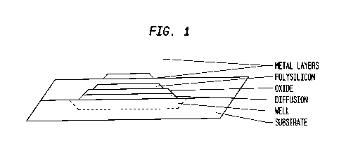
known method capable of removing the layers. Figure 1 shows some of the
semiconductor layers and regions that are imaged by the teardown reverse
engineering
technique.
Once the semiconductor device teardown is complete and the imaging information
is
gathered, the logic function of the device can be re-constructed by using
diffusion,
polysilicon, and well areas to define the MOS devices used to create logic
gates, and the
metal layers to define how the logic gates are interconnected. Figure 2 shows
how the
semiconductor layers define the MOS device.
U.S. Patent No. 7,711,964 discloses one method of protecting logic
configuration data.
The configuration data for the logic device is encrypted and a decryption key
is
encrypted using a silicon key. The encrypted decryption key and configuration
are
transferred to the logic device. The silicon key is used to decrypt the
decryption key
1
CA 02903372 2015-09-01
WO 2014/110384
PCT/US2014/011064
which is then used to decrypt the configuration data. One problem with this
method is
that the chip is not protected against physical reverse engineering as
described above.
Many other cryptography techniques are known. But, all cryptographic
techniques are
vulnerable to the conventional teardown techniques.
Disclosed is a method for designing a semiconductor device that is resistant
to these
techniques. The semiconductor device includes a physical geometry which is not
clearly
indicative of the device's function. For example, the semiconductor device is
designed
where two or more types of logic devices have the same physical geometry. When
the
tea rdown method is performed two or more devices will show the same physical
geometry, but, these two or more devices have different logic functions. This
prevents
the person performing the reverse engineering to determine the logic functions
by the
known methods of observing the geometry of the devices.
Employing the disclosed method and device will force the reverse engineer to
employ
more difficult techniques. These techniques are more time consuming, more
expensive,
and more likely to have errors.
SUMMARY
The present method and device presents a semiconductor device that it is
difficult to
reverse engineer using known techniques.
In one aspect of the present invention, a security device includes an
encryption circuit
for receiving an input of a first digital key and plaintext data, the
encryption circuit for
mathematically manipulating the digital key and the plaintext data to encrypt
the
plaintext data into encrypted data, wherein at least a portion of the
encryption circuit
comprises IBG circuitry. In another aspect of the present invention, a
security device
includes a decryption circuit for receiving an input of a second digital key
and the
encrypted data, the decryption circuit for mathematically manipulating the
digital key
and the encrypted data to decrypt the encrypted data into the plaintext data,
wherein at
least a portion of the decryption circuit comprises IBG circuitry
2
CA 02903372 2015-09-01
WO 2014/110384
PCT/US2014/011064
These and other features and objects of the invention will be more fully
understood
from the following detailed description of the embodiments, which should be
read in
light of the accompanying drawings.
In this regard, before explaining at least one embodiment of the invention in
detail, it is
to be understood that the invention is not limited in its application to the
details of
construction and to the arrangements of the components set forth in the
description or
illustrated in the drawings. The invention is capable of other embodiments and
of being
practiced and carried out in various ways. Also, it is to be understood that
the
phraseology and terminology employed herein, as well as the abstract, are for
the
purpose of description and should not be regarded as limiting.
As such, those skilled in the art will appreciate that the conception upon
which this
disclosure is based may readily be used as a basis for designing other
structures,
methods, and systems for carrying out the several purposes of the present
invention. It
is important, therefore, that the claims be regarded as including such
equivalent
constructions insofar as they do not depart from the spirit and scope of the
present
invention.
BRIEF DESCRIPTION OF THE DRAWINGS
The accompanying drawings, which are incorporated in and form a part of the
specification, illustrate embodiments of the present invention and, together
with the
description, serve to explain the principles of the invention;
FIG. 1 illustrates semiconductor layers and regions that are imaged by the
teardown
reverse engineering technique;
FIG. 2 illustrates how the semiconductor layers define the MOS device;
FIG. 3 illustrates a circuit that is resistive to conventional reverse
engineering
techniques;
FIG. 4 illustrates a circuit configuration using a comparator;
FIG. 5 illustrates a second configuration using a comparator;
3
CA 02903372 2015-09-01
WO 2014/110384
PCT/US2014/011064
FIG. 6 illustrates a circuit configuration without a comparator;
FIG. 7 illustrates a second circuit configuration without a comparator;
FIG. 8 illustrates an circuit configuration having six active devices;
FIG. 9A illustrates a multiplexer using the disclosed techniques;
FIG. 9B illustrates a second embodiment of a multiplexer using the disclosed
techniques;
FIG. 10 illustrates the implementation of a "NAND" logic function;
FIG. 11 illustrates the implementation of a "NOR" logic function;
FIG. 12 illustrates the implementation of a "INVERT" logic function;
FIG. 13 illustrates the implementation of a "BUFFER" logic function;
FIG. 14 illustrates the implementation of a "XOR" logic function;
FIG. 15 illustrates the implementation of a "XNOR" logic function;
FIG. 16A illustrates an IBG device having active components;
FIG. 16B illustrates alternative embodiments of IBG devices having active
components;
FIG. 17 illustrates a circuit comprised of resistors;
FIG. 18 illustrates a side view of a silicon wafer having active devices;
FIG. 19 shows 2 transistor (2T) IBG ROM circuit in accordance with one aspect
of the
present invention;
FIG. 20 shows a 2x2 array of a 2T IBG ROM in accordance with the present
invention;
FIG. 21 shows a functional block diagram of a 2T architecture ROM system in
accordance
with the present invention;
FIG. 22 shows an alternate embodiment of a 2T IBG ROM circuit in accordance
with the
present invention;
4
CA 02903372 2015-09-01
WO 2014/110384
PCT/US2014/011064
FIG. 23 shows 3 transistor (3T) IBG ROM bit-pair circuit in accordance with
one aspect of
the present invention;
FIG. 24 shows a functional block diagram of a 3T architecture ROM system in
accordance
with the present invention;
FIG. 25 shows a block diagram of an imaging cartridge chip including at least
one IBG
device in accordance with the present invention;
FIG. 26 shows a perspective view of an imaging cartridge chip including at
least one IBG
device attached to an imaging cartridge in accordance with the present
invention;
FIG. 27 shows a side sectional view of an exemplary CMOS pair including an IBG
device
in accordance with the present invention;
FIG. 28 shows a top plan view of the exemplary CMOS pair of FIG. 27;
FIGS. 29A and 29B show cross sectional views of an IBG fabrication that
illustrates the
transistor source/drain regions and associated implanted interconnects in
accordance
with the present invention;
FIGS. 30 and 31 illustrate an example of how IBG bit content can be programmed
to
change the logic function of an exemplary basic logic block in accordance with
the
present invention;
FIG. 32A is a plan view of the semiconductor device which appears to be a
field effect
transistor (FET);
FIGS. 32B, 32C, and 32D are cross sectional views of the semiconductor device
of FIG.
32A; and
FIGS. 33A and 33B show prior art devices;
FIG. 34 depicts artifact edges of a silicide layer of an IBG device in
accordance with the
present invention;
FIG. 35 shows an IBG circuit in accordance with the present invention;
5
CA 02903372 2015-09-01
WO 2014/110384
PCT/US2014/011064
FIGS. 36-38 show block diagrams of an IBG encryption and decryption system in
accordance with the present invention;
FIG. 39 shows an IBG protected secure video transmission system in accordance
with the
present invention;
FIG. 40 shows an IBG protected smart card system in accordance with the
present
invention;
FIG. 41 shows an IBG protected RFID system in accordance with the present
invention;
and
FIG. 42 shows a method of forming an IBG protected security system in
accordance with
the present invention;
FIG. 43 illustrates transmitting encrypted data and decrypting the data.
DETAILED DESCRIPTION OF THE DRAWINGS
Many semiconductor processes that contain logic functions provide different
types of
metal-oxide-semiconductor (MOS) devices to be used in different environments.
For
example, one device can operate only at lower voltages and can be sized to
minimum
geometry. Another device can operate at higher voltages and cannot be sized to
minimum geometry. Using this type of device allows the semiconductor device to
interface to external signals that are higher in voltage when compared to the
internal
minimum sized devices.
The type of MOS device in the previous example is typically controlled by the
electrical
characteristics of the diffusion material. These characteristics are changed
by slightly
altering the atomic structure of this material by using an ion implant dose
and energy.
This process is normally described as "doping". This slight change of
electrical properties
cannot be detected by the conventional reverse engineering teardown
techniques.
In order to provide a device that is resistant to these reverse engineering
techniques, an
invisible bias generator (IBG) has been developed. An IBG may be defined as an
electronic device having at least two internal devices where the physical
geometries of
6
CA 02903372 2015-09-01
WO 2014/110384
PCT/US2014/011064
the internal devices cannot be used to determine the operating characteristics
of the
IBG.
One example of an IBG is a device where both internal devices have the same
geometry
but operate differently. For example, the first device may be a transistor
that operates
at a first voltage level and the second device is a transistor that operates
at a different
voltage level. In another example, the first device is a silicide resistor
while the second
device is a non-silicide resistor. In another example, conductive ink is used
to create an
electronic circuit and the amount of conductive material in the ink is changed
between
two of the elements.
Another example of an IBG is a device where both internal devices have
different
geometries but have the same operating characteristics. For example, the first
device
may be a transistor that operates with first characteristics and the second
device is
larger a transistor that operates with the same characteristics. In another
example, the
first device is a silicide resistor while the second device is a non-silicide
resistor. In
another example, conductive ink is used to create an electronic circuit and
the amount
of conductive material in the ink is changed between two of the elements.
Another example of an IBG circuit includes devices having multiple possible
geometries
and multiple possible operating characteristics, with no apparent correlation
existing
between a given geometry and an operating characteristic.
FIG. 3 illustrates an exemplary IBG circuit 300 that provides an effective
deterrent to
semiconductor device teardown techniques. The circuit300 includes a first IBG
device
comprising a P-channel device301 and an N-channel device 303 which are
connected in
series between a power source (VCC) and a ground. A second IBG device
comprises a P-
channel device 302 and an N-channel device 304 also connected in series
between VCC
and ground. In one aspect of the present invention, the devices 301-304 may
comprise
MOS transistors. In a preferred embodiment, the devices 301-304 may also
exhibit
identical device geometry. The gates on the P-channel devices 301, 302 are
floating as
they not provided with an input signal (floating gates) and are charged via
leakage
current to a voltage level approximately VCC minus the threshold voltages of
the devices
301 and 302, each of the threshold voltages is independent. The gates on the N-
channel
7
CA 02903372 2015-09-01
WO 2014/110384
PCT/US2014/011064
devices 303, 304 are also floating gates and are charged via leakage current
to a voltage
level of approximately ground plus the threshold voltages of the devices 303
and 304.
Each device 301-304 may include a conduction channel between a source and a
drain of
the device. The depth of the conduction channel is determined by the doping
levels of
the diffusion(also known as implantation) areas of the gates of devices 301-
304 which in
turn determine the voltage level on the P and N channel device junctions,
labeled VA
and VB in FIG. 3.In one aspect of the present invention, the devices 301-304
are formed
with different doping levels (also called impurity levels)between at least
some of the
devices 301-304 while maintaining identical device geometry, thus resulting in
the
device junctions VA and VB having different voltage levels. A comparator 310
detects
the voltage levels of VA and VB and based on the difference in these voltage
bias levels
outputs a logical"1" or "0". VA and VB can be any voltage level as the logic
criteria of
the comparator 310is based on the difference of these voltages. In a preferred
embodiment, the circuit of FIG. 3 contains identical geometry for the P and N
channel
devices 301-304, thus causing the doping level difference between the devices
301-304
to control the difference in the voltage levels of the device junctions VA and
VB. For
example, if devices 301 and 303 are doped to form low voltage MOS transistors
(such as
2.5V, for example) and if devices 302 and 304 are doped differently to form
high voltage
MOS transistors (such as 3.3V, for example), then device junction VA is at a
higher
voltage than device junction VB, and the output of the comparator will be a
logical "1".
As another example, if devices 301 and 304 are doped to form low voltage MOS
transistors, and if devices 302 and 303 are doped to form high voltage MOS
transistors,
then device junction VA is at a lower voltage than device junction VB, and the
output of
the comparator will be a logical "0". The logic function of this circuit is
invisible to
reverse engineering teardown techniques since the operating voltages of the
device
junctions VA and VB are controlled by the doping levels and these doping
levels are not
determinable by conventional techniques.
For semiconductor technologies which provide different types of MOS devices,
such as
the high and low voltage devices described above, an advantage of the IBG
circuit is that
it can be easily constructed with current methods. Also, an IBG circuit in
accordance
8
CA 02903372 2015-09-01
WO 2014/110384
PCT/US2014/011064
with one aspect of the present invention can be used to create a number of
different of
logic cells by varying the number of high voltage devices and low voltage
devices.
FIG. 4 shows an exemplary circuit 420 including an IBG and a level shifter
circuit which
produces a logical "1", or high, output in accordance with one aspect of the
present
invention. The IBG portion of the circuit 420 comprises transistors 401, 402,
405, and
406 each having a floating gate input.P-channel transistor 401 is connectedin
series with
N-channel transistor 405 at output node 401A, and P-channel transistor 402 is
connected in series with N-channel transistor 406 at output node 402A. Each of
the
transistors of the IBG portion of the circuit can be a P-type or an N-type
device. Also
each transistor can be a high voltage device or a low voltage device. In a
preferred
embodiment, a high voltage device operates at 3.3 V while a low voltage device
operates at 2.5 V. In an exemplary embodiment, transistor 402 is a low voltage
P-type
device,transistor 401 is a high voltage P-type device,transistor405is a low
voltage N-type
device, and transistor 406is a high voltage N-type device, resulting in the
voltage level at
output node 402A being higher than the voltage level at the output node
401A.For
example, transistors 401 and 405 may produce a voltage level of about 100mV at
the
output node 401A and transistors 402 and 406 may produce a voltage level of
about 1.5
V at the output node 402A. These output levels fall short of being VCC and
ground due
to transistors 401, 402, 405, and 406 not being fully turned ON or OFF by the
charge on
their floating gates which are charged by leakage currents. Transistors 401,
402, 405
and 406 are selected to ensure the voltage levels of the output nodes 401A and
402A
are such the one voltage level is higher and the other voltage level is lower
than the
threshold voltage of transistors 407 and 408, described below.
The voltage levels of the output nodes 401A and 402A of the IBG circuit are
insufficient
to interface directly with digital logic due to the voltage level of the gates
of the
transistors 401, 402, 405 and 406.To properly interface with digital logic,
the signals
from the output nodes 401A and 402A are input to a level shifting circuit
comprisingtransistors 403, 404, 407 and 408. Transistors 403 and 404 may
comprise low
voltage P-type devicesand transistors 407 and 408 may comprise low voltage N-
type
devices. The output node 401A of the IBG circuitis connected to the gate of N-
channel
transistor 408 of the level shifting circuit and the output node 402A of the
IBG circuit is
9
CA 02903372 2015-09-01
WO 2014/110384
PCT/US2014/011064
connected to the gate of the N-channel transistor 407 of the level shifting
circuit.ln an
exemplary embodiment, the N-channel transistors may have a threshold voltage
of
about 700 mV. Thus, the 100 mV voltage level of node 401A which is input to
the gate
of transistor 408 will turn transistor 408 "OFF" and the 1.5 V voltage level
which is input
to the gate of transistor 407 will turn transistor 407 "ON". Thus, transistor
403 will be
turned "OFF" and transistor 404 will be turned "ON", resulting in the output
of the level
shifting circuit being a logical "1" or HI.
FIG. 4 also shows also an exemplary circuit 430 including an IBG and level
shifting circuit
which produces a logical "0", or low, output in accordance with one aspect of
the
present invention. The IBG portion of the circuit 420 comprises transistors
409, 410,
413, and 414 each having a floating gate input. P-channel transistor 409 is
connected in
series with N-channel transistor 413 at output node 409A, and P-channel
transistor 410
is connected in series with N-channel transistor 414 at output node 410A. Each
of the
transistors of the IBG portion of the circuit can be a P-type or an N-type
device. Also
each transistor can be a high voltage device or a low voltage device. In a
preferred
embodiment, a high voltage device operates at 3.3 V while a low voltage device
operates at 2.5 V. In an exemplary embodiment, transistor 409 is a low voltage
P-type
device, transistor 410 is a high voltage P-type device, transistor 413 is a
high voltage N-
type device, and transistor 414 is a low voltage N-type device, resulting in
the voltage
level at output node 409A being higher than the voltage level at the output
node
410A.For example, transistors 410 and 414 may produce a voltage level of about
100 mV
at the output node 410A and transistors 409 and 413 may produce a voltage
level of
about 1.5 V at the output node 409A. Transistors 409, 410, 413 and 414 are
selected to
ensure the voltage levels of the output nodes 409A and 410A are such the one
voltage
level is higher and the other voltage level is lower than the threshold
voltage of
transistors 415 and 416, described below.
The voltage levels of the output nodes 409A and 410A of the IBG circuit are
insufficient
to interface directly with digital logic due to the voltage level of the gates
of the
transistors 409, 410, 413 and 414. To properly interface with digital logic,
the signals
from the output nodes 409A and 410A are input to a level shifting circuit
comprising
transistors411, 412, 415 and 416. Transistors 411 and 412 may comprise low
voltage P-
CA 02903372 2015-09-01
WO 2014/110384
PCT/US2014/011064
type devices and transistors 415 and 416 may comprise low voltage N-type
devices. The
output node 409A of the IBG circuit is connected to the gate of N-channel
transistor 416
of the level shifting circuit and the output node 410A of the IBG circuit is
connected to
the gate of the N-channel transistor 415 of the level shifting circuit. In an
exemplary
embodiment, the N-channel transistors may have a threshold voltage of about
700 mV.
Thus, the 1.5 V voltage level of node 409A which is input to the gate of
transistor 416
will turn transistor 416 "ON" and the 100mV voltage level which is input to
the gate of
transistor 415 will turn transistor 415 "ON". Thus, transistor 412 will be
turned "OFF"
and transistor 411 will be turned "ON", resulting in the output of the level
shifting circuit
being a logical "0" or LO.
As described above, the circuit420 gives the "Hl" voltage output while
circuit430 gives
the "LO" voltage output. The geometry and size of the IBG transistors 401,
402, 405
and 406 of the circuit420may be identical to the geometry and size of the IBG
transistors
409, 410, 413 and 414 of thecircuit430. The only discernable difference
between the
two devices is the level of doping between the high voltage transistors and
the low
voltage transistors. Because the size and the geometry of IBG transistors of
device
420may be identical to the IBG transistors of device 430, it is not possible
to determine
the difference between these two devices using the conventional reverse
engineering
teardown techniques.
FIG. 5 illustrates a second example of IBG circuits and level shifting
circuits to output a
"Hl" or "LO" output. Similar to the embodiment shown in FIG. 4, there are 16
transistor
devices (501 through 516). Each of the transistors can be a P-type or an N-
type device.
Also each device can be a high voltage device or a low voltage device. In a
preferred
embodiment, a high voltage device operates at 3.3 V while a low voltage device
operates at 2.5 V. In an exemplary embodiment, transistors 502, 503, 504, 509,
511,
and 512 are low voltage P-type devices. Transistor 501 and 510 are high
voltage P-type
devices. Transistors 505, 507, 508, 514, 515, and 516 are low voltage N-type
devices.
Transistors 506 and 513 are high voltage N-type devices. Device 520 gives the
"Hl"
voltage output while device 530 gives the "LO" voltage output. The geometry
and size
of the IBG transistors 501, 502, 505, and 506 of the device 520may be
identical to the
geometry and size of transistors 509, 510, 513 and 514 of device 530. The only
11
CA 02903372 2015-09-01
WO 2014/110384
PCT/US2014/011064
discernable difference between the two devices is the level of doping between
the high
voltage transistors and the low voltage transistors. Because the size and the
geometry
ofthe IBG transistors ofdevice 520 is identical to that of the IBG transistors
of device 530
it is not possible to determine the difference between these two devices using
the
conventional reverse engineering teardown techniques.
If a semiconductor chip contains an IBG as described in FIG. 4 or FIG. 5, it
is extremely
difficult for someone trying to reverse engineer the chip using teardown
techniques to
determine the function of the IBG devices placed on the chip because the
geometry of
the internal devices are the same.
FIG. 6 and FIG. 7 illustrate examples of IBGs where the voltage levels of the
outputs of
the circuits are sufficient to directly interface with the devices on a chip.
In FIG. 6,
device 601 is a high voltage P-type device, such as 3.3v, device 602 is a low
voltage P-
type device, such as 2.5v, device 603 is a low voltage N-type device and 604
is a high
voltage N-type device. By connecting the gate of device 601 to the gate of
device 602,
these devices share the leakage current, resulting in the high voltage device
601 being
fully turned OFF and the low voltage device 602 being fully turned ON.
Similarly, by
connecting the gate of device 603 to the gate of device 604, these devices
share the
leakage current, resulting in the low voltage device 603 being fully turned ON
anddevice
604 being fully turned OFF. Output node 601A will be sufficiently close to
ground to
function as a logical "0" and interface directly with other CMOS devices and
output node
602A will be sufficiently close to VCC to function as a logical "1" and
interface directly
with other CMOS devices.
In FIG. 7, device 701 is a low voltage P-type device, such as 2.5 V, device
702 is a high
voltage P-type device, such as 2.5 V, device 704 is a low voltage N-type
device and 703 is
a high voltage N-type device. By connecting the gate of device 701 to the gate
of device
702, these devices share the leakage current, resulting in the low voltage
device 701
being fully turned ON and the high voltage device 702 being fully turned OFF.
Similarly,
by connecting the gate of device 703 to the gate of device 704, these devices
share the
leakage current, resulting in the high voltage device 703 being fully turned
OFF and low
voltage device 704 being fully turned ON. Output node 701A will be
sufficiently close to
12
CA 02903372 2015-09-01
WO 2014/110384
PCT/US2014/011064
VCC to function as a logical "1" and interface directly with other CMOS
devices and
output node 702A will be sufficiently close to ground to function as a logical
"0" and
interface directly with other CMOS devices.
The geometry and size of the IBG transistors 601, 602, 603 and 604 may be
identical to
the geometry and size of the IBG transistors 701, 702, 703 and 704 The
geometry and
size of IBG transistors 601, 602, 603, and 604 may not be identical to each
other. The
geometry and size of IBG transistors 701, 702, 703 and 704 may not be
identical to each
other. Additionally, the voltage levels at the gates of the gate connected
transistors are
equal. The only discernible difference between the two devices is the level of
doping
between the high voltage transistors and the low voltage transistors. Because
the size
and the geometry of IBG transistors of Fig. 6 may be identical to the IBG
transistors of
device Fig. 7, it is not possible to determine the difference between these
two devices
using the conventional reverse engineering teardown techniques. The IBG shown
in FIG.
6 has the same geometry as the IBG shown in FIG. 7 with the only difference
being the
doping level of some of the transistors. Therefore, if a chip is designed
using the IBG
illustrated in FIG. 6 and the IBG illustrated in FIG. 7, it is very difficult
to determine a
difference in the function of the devices made by each design.
The IBG shown in FIG. 6 can include different configurations. In one example,
device 601
is a low voltage P-type device, device 602 is a high voltage P-type device,
device 603 is a
low voltage N-type device and 604 is a high voltage N-type device. In another
example
device 601 is a high voltage P-type device, device 602 is a low voltage P-type
device,
device 603 is a high voltage N-type device and 604 is a high voltage N-type
device. In
another example device 601 is a high voltage P-type device, device 602 is a
low voltage
P-type device, device 603 is a low voltage N-type device and 604 is a low
voltage N-type
device. In another example device 601 is a high voltage P-type device, device
602 is a
low voltage P-type device, device 603 is a low voltage N-type device and 604
is a high
voltage N-type device. There are a total of sixteen configurations possible
for a four
device IBG.
FIG. 8 illustrates another embodiment of an IBG circuit. Devices 801, 802, 803
are
shown as P-type devices and can be any combination of high voltage or low
voltage
13
CA 02903372 2015-09-01
WO 2014/110384
PCT/US2014/011064
devices. Devices 804, 805, 806 are shown as N-type devices and can be any
combination
of high voltage or low voltage devices. However, the six devices shown can be
any
combination of P-type and N-type devices. The six device IBG has a total of 64
possible
configurations. Furthermore, an IBG can be comprised of any number of active
devices
with 2 to the "n" number of combinations, where n is the number of active
devices.
FIG. 9A and FIG. 9B illustrate IBG circuits which include multiplexers.
Because IBG
circuits may be used to select logic functions, it is convenient to implement
these circuits
in conjunction with digital multiplexers that effectively steer one of two
inputs to its
output. These IBG based multiplexers select an input base solely on the IBG
function. In
Fig. 9A, transistors 901, 902, 905 and 906 comprise an IBG circuit and
transistors 903,
904, 907 and 908 comprise a multiplexer. In Fig. 9B, transistors 911, 912, 915
and 916
comprise an IBG circuit and transistors 917, 918, 913 and 914 comprise a
multiplexer. In
FIG. 9A, devices 901 and 906 are 3.3V devices while devices 902, 903, 904,
905, 907, and
908 are 2.5V devices. Inverter 910 provides the inverse of input A and the
inverse of
input B. In FIG. 9B, devices 912 and 915 are 3.3V devices while devices 911,
913, 914,
916, 917, and 918 are 2.5V devices. Inverter 920 provides the inverse of input
A and the
inverse of input B. Based on the outputs of the IBG transistors 901, 902, 905
and 906,
the multiplexer shown in FIG. 9A selects the B input while the multiplexer
shown in
FIG.9B selects the A input based on the outputs of the IBG transistors 911,
912, 915 and
916. The only discernible difference between the two devices is the level of
doping
between the high voltage transistors and the low voltage transistors. Because
the size
and the geometry oftransistors of Fig. 9A may be identical to the transistors
of Fig. 9B, it
is not possible to determine the difference between these two devices using
the
conventional reverse engineering teardown techniques. The IBG shown in FIG. 9A
may
have the same geometry as the IBG shown in FIG. 9B with the only difference
being the
doping level of some of the transistors. Therefore, if a chip is designed
using the circuit
illustrated in FIG. 9A and the circuit illustrated in FIG. 9B, it is very
difficult to determine
a difference in the function of the devices made by each design.The only
difference
between these circuits is the configuration of 3.3V and 2.5V devices.
FIG. 10 represents the implementation of a "NAND" logic function and FIG. 11
illustrates
the implementation of a "NOR" logic function. In FIG. 10, NAND gate 1010 and
14
CA 02903372 2015-09-01
WO 2014/110384
PCT/US2014/011064
NORgate1011 output to an IBG based multiplexer1012, such as the IBGcircuit
multiplexer shown in Fig. 9A, which selects the output of the NAND gate 1010.
In FIG.
11, NANDgate1110 and NORgate1111 output to an IBG based multiplexer1112, such
as
the IBG circuit multiplexer shown in Fig. 9B, which selects the output of the
NOR gate
1111. These two implementations appear to identical during reverse engineering
because the difference between these configurations is the IBG circuit.
Without
knowledge of the IBG circuit the logic function of these configurations is
indeterminate.
FIG. 12 illustrates an implementation of the logic function "INVERT"
comprising an
inverter 1201 and an IBG based multiplexer 1202, such as the IBG circuit
multiplexer
shown in Fig. 9A, implemented to select the inverted input. FIG. 13
illustrates an
implementation of the logic function "BUFFER" comprising an inverter 1301 and
an IBG
based multiplexer 1302, such as the IBG circuit multiplexer shown in Fig. 9B,
implemented to select the non-inverted input.FIG. 14 illustrates an
implementation of
the logic function "XOR" comprising an exclusive-or gate 1401, an inverter
1403 and an
IBG based multiplexer 1402, such as the IBG circuit multiplexer shown in Fig.
9A,
implemented to select the output of the gate 1401. FIG. 15 illustrates an
implementation of the logic function "XNOR" comprising an exclusive-nor gate
1501, an
inverter 1503 and an IBG based multiplexer 1502, such as the IBG circuit
multiplexer
shown in Fig. 9B, implemented to select the output of the inverter 1503. As
with the
previous examples, reverse engineering a chip that has both the "INVERT" of
FIG. 12 and
the "BUFFER" of FIG. 13 will be difficult to perform because the "INVERT" and
the
"BUFFER" will have the same appearance. Reverse engineering a chip that has
both the
"XOR" of FIG. 14 and the "XNOR" of FIG. 15 is difficult because the "XOR" and
"XNOR"
have the same appearance. As described above, each pair of implementations is
indeterminate without knowledge of the logical operation of the IBG circuit
based
multiplexers.
One advantage of the high voltage / low voltage method of anti-reverse
engineering
deterrent is that most processes support this distinction. Many
implementations are
designed to use low voltages internal voltages because as feature size
decreases the
internal voltage decreases. But, many devices outside of the chip operate at
higher
voltages and the chips must be able to interface with these devices.
Therefore, devices
CA 02903372 2015-09-01
WO 2014/110384
PCT/US2014/011064
that use higher voltages are still used and being developed. It is possible to
for the
difference between the low voltage device and the high voltage device to be
achieved
using small doping changes between P and N devices.
The IBG devices described above include active devices that use the dopant
level to
control characteristics of the devices. As an example, it is known in a
particular process
that a doping concentration difference between the 2.5V and 3.3V devices is
about
8xE16 atoms/cm3. Structures that have doping density differences below 1xE17
are
candidates for IBG design. Examples of IBGs are in FIG. 16.
There are many other combinations of devices that will work besides the 2.5V
and 3.3V
devices. For example, a 2.5V can be used with a 5V device. A 1.8V device, a
1.5V device,
or a 1.2V can be used with a 3.3V device. A 1.2V device can be used with 1.8V
or a 2.5V
device. A 1.0V device can be used with a 1.8V device, 2.5V device, or a 3.3V
device. A
0.85V device can be used with a 1.8V device, a 2.5V device, or a 3.3V device.
This list is
exemplary only and any combination of devices that can be made with the same
physical geometry can be used.
The previous examples illustrate some of the possible implementations of IBG
devices
using active devices. Another way to achieve an IBG device is to use inactive
devices.
The IBG can be made using a silicide poly resistor and a non-silicide poly
resistor. The
first device is used to set the first bias voltage as an active bias voltage
and the second
device is used to set the set the second bias voltage as an active bias
voltage. The
difference between the silicide poly resistor and the non-silicide poly
resistor will not be
apparent to the conventional reverse engineering techniques because the
resistors have
the same geometry. FIG. 16A illustrates an example of an IBG device. FIG. 16B
illustrates other examples of an IBG device.
Polysiliconhas fairly high resistivity, about a few hundred un-cm. Resistive
devices from
polysilicon suffer from this high resistivity because as the device dimension
shrinks the
resistance of the polysilicon local interconnection increases. This increased
resistance
causes an increase in the power consumption and a longer RC time
delay.Silicides are
added to polysilicon devices because the addition of the silicides reduces the
resistance
and increases device speed. Any silicide that has a much lower resistivity
than
16
CA 02903372 2015-09-01
WO 2014/110384
PCT/US2014/011064
polysilicon may be used. Titanium silicide (TiSi2) and tungsten silicide
(WSi2) are two
suicides that are commonly used.
Next, one method of forming a silicide device is described. A self-aligned
silicide process
is conventionally used to from Titanium Silicide. Initially, chemical
solutions are used to
clean the wafer surface in order to remove contaminants and particles. Next,
the wafer
is sputtered in a vacuum chamber using argon to remove the native oxide from
the
wafer surface. Next, a layer of the wafer surface is sputtered to deposit a
layer of
titanium on the wafer surface. This results in a wafer having the silicon
exposed at the
source/drain and on top of the polysilicon gate. Next, a titanium silicide is
formed on
the polysilicon by using a thermal annealing process. For example, annealing
can be
performed in a rapid thermal process to form titanium silicide on top of the
polysilicon
and on the surface of the source/drain. Because titanium does not react with
silicon
dioxide, silicide is formed only where polysilicon directly contacts with
titanium. Next,
the unreacted titanium is removed by using a wet etch process that exposes the
unreacted titanium to a mixture of hydrogen peroxide (H202) and sulfuric acid
(H2SO4).
Lastly, the wafer is annealed which increases the grain size of the titanium
Silicide. The
increased grain size improves the wafer's conductivity and reduces wafer's
contact
resistance.
Another characteristic that can be controlled in the IBG device is the
threshold voltage.
The threshold of MOS transistors can be controlled by threshold adjustment
implant. An
ion implantation process is used to ensure that the power supply voltage of
the
electronic systems can turn the MOS transistor in the IC chip on and off. The
threshold
adjustment implantation is a low-energy and low current implantation process.
Typically, the threshold adjustment implantation is performed before gate
oxide growth.
For CMOS IC chips, two threshold adjustment implantation processes are needed,
one
for p-type and one for n-type.
In an IBG device, the process described above can be used to produce resistors
that have
the same physical dimensions and have different resistance. Conversely, the
process
can be used to produce resistors that have different geometries and the same
resistance.
17
CA 02903372 2015-09-01
WO 2014/110384
PCT/US2014/011064
FIG. 17 illustrates an example of an IBG device implemented by silicide
resistors. A
voltage source VCC is connected to a circuit having resistors 1701, 1702,
1703, 1704.
The resistance of the resistors can be set by the method described above to
have two
different resistance levels with all of the resistors having the same physical
geometry.
For example, resistors 1701 and 1704 may be non-silicide resistors while
resistors 1702
and 1703 are silicide resistors. In this example if Va is less than Vb then
the output of
the device is a logic "1." If Va is greater than or equal to Vb then the
output of the
device is a logic "0."
In another embodiment, the devices can be formed using conductive inks.
Conductive
inks are used to print circuits on a variety of substrate materials.
Conductive inks
contain conductive materials such as powdered or flaked silver materials.
Conductive inks can be used to implement IBG circuits because the properties
of the inks
used to print the circuit can be varied to create devices that have different
properties.
For example, some devices can be printed using conductive ink having an amount
of
conductive material. Then, conductive ink that has more (or less) conductive
material is
used to print another portion of the circuit. The circuit then can have
devices that look
similar and operate differently or look different and operate the same.
One possible method of reverse engineering IBG circuits is to physically
measure the
devices in the circuit. This can be done using a probe to measure the actual
voltage
generated by the circuit. In order to thwart this method of reverse
engineering, the IBG
cells are placed randomly spaced throughout the design. This makes it more
difficult to
probe the large number of IBG circuits required to reverse engineer the
design.
In an alternative embodiment, the types of IBG circuits used are randomly
distributed.
For example, every third "AND" gate is implemented using an IBG circuit while
every
fourth "NAND" gate is implemented using an IBG circuit. As the number of
devices
implemented by IBG circuits is increased, the difficulty in reverse
engineering the chip is
increased. Additionally, as the number of types of logic devices implemented
by IBG is
increased, the difficulty in reverse engineering the chip is increased.
18
CA 02903372 2015-09-01
WO 2014/110384
PCT/US2014/011064
In another embodiment, logic blocks are made having logic devices therein.
Within each
logic block, the IBGs are randomly distributed within the logic block. As a
result,
different types of logic devices within each logic block are comprised of IBG
devices.
In another embodiment, logic blocks are made having logic devices. The
designer
determines for the logic blocks a critical point and uses an IBG to implement
the critical
point. The critical point is a point within the logic the block where it is
necessary to
know the function or output value in order to determine the function of the
logic block.
Implementing the critical point within the logic block by an IBG is
advantageous because
this ensures that IBG has maximum effect in preventing reverse engineering.
The
inability to determine the value of critical point will necessarily prevent
the reverse
engineer from determining the proper function for the logic block.
For example, if the logic block is an ADDER, replacing a digit in the output
can make it
impossible to determine the function of the adder. That is because someone
trying to
reverse engineer the chip monitoring the function of the logic block would
expecta
specific output for an ADDER. When the replaced digit does not give the
expected
result, it is not determined that the logic block is functioning as and ADDER.
Another advantage of the disclosed system and method is that chip can be
designed
using standard tools and techniques. Methods of designing a chip are described
in the
following paragraphs.
A designer creates an overall design for the chip and for logic blocks within
the chip. The
design is created in a known hardware design language such as Verilog or VHDL.
The
design is then synthesized into standard logic which converts the design to
the
optimized gate level. Synthesis may be performed using standard synthesis
tools such
as Talus Design, Encounter RTL Designer, and Design Compiler. The synthesis
maps the
logic blocks into standard logic using a standard cell library provided by the
supplier.
Next, a place and route tool is used to create a physical implementation of
the design.
This step involves creating a floorplan, a power grid, placing the standard
cells,
implementing a clock tree, and routing connectivity between cells and
input/output
pins. Some examples of place and route tools are Talus Vortex, Encounter
Digital
Implementation, and IC Compiler. Using this process there are various ways to
design a
19
CA 02903372 2015-09-01
WO 2014/110384
PCT/US2014/011064
chip using IBG devices. One way is to create and characterize one or more new
standard
cell libraries and use the one or more new standard cells at the beginning of
the process.
Another approach is to place the IBG devices during the place and route step,
either
automatically or manually.
Another method of designing a chip is for the designer to create the design
using a
schematic entry tool. The designer creates a circuit by hand comprising the
base logic
gates. The designer can optimize the logic functionality using Karnaugh-maps.
A layout
entry tool is used to create the physical implementation of the design. The
designer
draws polygons to represent actual layers that are implemented in silicon.
Using this
approach the designer places IBG devices at any desired location.
Because the above devices result in a design that is difficult to reverse
engineer using
the conventional tear down techniques, another method may be implemented to
reverse engineer the chip. Another known method of reverse engineering is to
probe
the device while active in order to establish the operating values of the
internal devices.
In order to perform these methods, the reverse engineer must remove some
layers of
the wafer to expose the output contacts of the devices. One way to make this
technique
more difficult is to randomly place the logic devices as described above.
Another
technique is to design a chip that is physically resistant to these
techniques.
FIG. 18 illustrates the layers of a silicon wafer that is resistant to
electronic testing of the
chip. The wafer has a base layer 1801 that includes the diffusion layer. The
oxide layer
1802 is on top of the diffusion layer 1801. The polysilicon layer 1803 is
located on top of
the oxide layer with the metal layer 1 1804 located thereon. The signal
outputs are
formed in metal layer 1 1804. Metal layer 2 1805 is located on top of the
metal layer 1
1804. The gate connections are formed in metal layer 2 1805. With this layout
it is
necessary to remove a portion of metal layer 2 1805 in order to probe the
signal outputs
that are located in metal layer 1 1804. Removing a portion of metal layer 2
1805
disrupts the gate connections of the devices which in turn deactivates the
devices. Thus,
a reverse engineer trying to probe the device will destroy the functionally of
the device
during the reverse engineering process.
CA 02903372 2015-09-01
WO 2014/110384
PCT/US2014/011064
In many of the techniques described above, the output voltage level of a
device is used
to determine the operation of the device. But, any other operating
characteristic of the
device could be used. For example, the rise time of the device, the current
drawn, or
the operating temperature can be used in the IBG. Also, more than one physical
property of the device can be varied. For example, the geometry and the doping
level
can be controlled to implement an IBG.
Another advantage of the disclosed system and method is that it can be
implemented in
any type of electronic device. For example, a read-only memory (ROM) can be
implemented with the techniques described above and the contents of the memory
are
protected by the physical implementation of the IBG circuit. This enables a
protected
memory device without the need for complicated encryption techniques.
An IBG ROM circuit may be a masked memory technology that is highly resistant
to
hardware reverse engineering techniques. The IBG ROM circuit may be based on
bit
pairing of N and P channel devices with doping density differences too small
to small to
be determined by optical differentiation techniques. The IBG ROM increases the
complexity and cost of reading out memory using optical reverse engineering
processes,
thus producing a secure environment for the data stored in the IBG ROM.
FIG. 19 shows 2 transistor (2T) IBG ROM circuit 1900 in accordance with one
aspect of
the present invention. The 2T IBG ROM circuit 1900 includes a first N channel
transistor
1902 having an output node 1904 connected to the source terminal of the N
channel
transistor 1902. The N channel transistor 1902 is selected to have a device
geometry
and device characteristics, including doping characteristics, adapted to bias
the output
node 1904 at a predetermined voltage level indicating a binary 1 or a
predetermined
voltage level indicating a binary 0 when the N channel transistor 1902 is
connected to a
P channel device, described in greater detail below. The doping characteristic
differences between a binary 1 and a binary 0 are too small to be detected by
optical
techniques. The gate terminal of the first N channel transistor 1902 is a
floating gate
and thus not connected to an input signal. The drain terminal of the first N
channel
transistor 1902 is connected to ground. The 2T IBG ROM circuit 1900 also
includes a
second N channel transistor 1906 connected between the output node 1904 and a
data
21
CA 02903372 2015-09-01
WO 2014/110384
PCT/US2014/011064
bus 1908. A word line 1910 is connected to the gate of the N channel
transistor 1906.
The N channel transistor 1906 operates as pass transistor and is turned ON by
the word
line 1910. When the pass transistor 1906 is turned ON by the word line 1910,
the pass
transistor passes the predetermined voltage level of the output node 1904 to
the data
bus 1908.
A common P channel circuit 1910 is also connected to the data bus and provides
the
leakage current to charge the floating gate in the first N channel transistor
1902 when
the pass transistor 1906 is turned ON. The common P channel circuit 1910
includes a P
channel transistor 1912 and a dummy P and N transistor pair 1914 connected in
series.
The gates of the P channel transistor 1912 and the dummy P transistor are
connected,
creating the leakage profile required for proper operation of the first N
channel
transistor 1902 when the pass transistor 1906 is turned ON. The predetermined
voltage
level will only be present at the output node 1904 when the pass transistor
1906 is
turned ON and thus connecting the common P channel circuit 1910 to the
transistor
1902 to provide the leakage current for the operation of the N channel
transistor 1902.
FIG. 20 shows a 2x2 array of a 2T IBG ROM 2000 in accordance with the present
invention. The 2x2 IBG ROM includes four N channel transistors 2002, 2004,
2006 and
2008 and their associated pass transistors 2012, 2014, 2016 and 2018. The four
N
channel transistors 2002, 2004, 2006 and 2008 have output nodes 2003, 2005,
2007 and
2009. The N channel transistors 2002, 2004, 2006 and 2008 are selected to have
device
geometries and device characteristics, including doping characteristics,
adapted to bias
the output nodes 2003, 2005, 2007, and 2009 at predetermined voltage levels
indicating
a binary 1 or a predetermined voltage level indicating a binary 0 when the N
channel
transistors 2002, 2004, 2006 and 2008 is connected to a P channel device,
described in
greater detail below. The doping characteristic differences between a binary 1
and a
binary 0 are too small to be detected by optical techniques. Transistors 2002
and 2004
are both part of a first word, and their pass transistors 2012 and 2014 are
turned ON by
a first word line 2020. Transistors 2006 and 2008 are both part of a second
word, and
their pass transistors 2016 and 2018 are turned ON by a second word line 2022.
The
output of pass transistors 2012 and 2016 are connected to a first data bus
2030 and the
output of pass transistor 2014 and 2018 are connected to a second data bus
2032.
22
CA 02903372 2015-09-01
WO 2014/110384
PCT/US2014/011064
When the word line 2020 is asserted the pass transistors 2012 and 2014 are
turned ON
and the pass transistors 2012 and 2014 pass the predetermined voltage levels
of the
output nodes 2003 and 2005 to the data buses 2030 and 2032. When the word line
2022 is asserted the pass transistors 2016 and 2018 are turned ON and the pass
transistors 2016 and 2018 pass the predetermined voltage levels of the output
nodes
2007 and 2008 to the data buses 2030 and 2032.
A first common P channel circuit 2040 is connected to the first data bus 2030
and
operates as the common P channel for transistors 2002 and 2006, and a second
common P channel circuit 2042 is connected to the second data bus 2032 and
operates
as the common P channel for transistors 2014 and 2018. The predetermined
voltage
level will only be present at the output nodes 2003 and 2005 when the pass
transistors
2012 and 2014 are turned ON and thus connecting the common P channel circuit
2040
to the transistors 2002 and 2004 to provide the leakage current for the
operation of the
N channel transistors 2002 and 2004. Similarly, the predetermined voltage
level will only
be present at the output nodes 2007 and 2009 when the pass transistors 2016
and 2018
are turned ON and thus connecting the common P channel circuit 2042 to the
transistors
2006 and 2008 to provide the leakage current for the operation of the N
channel
transistors 2006 and 2006.
FIG. 21 shows a functional block diagram 2100 of a 2T architecture ROM system
in
accordance with the present invention. An address decode 2102 unit receives
the
address to be read from an external system and decodes this address to select
a word
line which corresponds the word of data to be read from the IBG N channel
device array
2104. Common P channel devices 2106 are connected to each data line output
2104. A
read amplifier 2108 amplifies the word of data output to convert the word of
data from
voltage levels output the array 2104 to levels that correspond to logical "1"
and logical
"0" in digital logic circuits. The read amplifier transmits the amplified data
on a data bus
2110.
FIG. 22 shows an alternate embodiment of a 2T IBG ROM circuit 2200 in
accordance with
the present invention. In contrast to the 2T IBG ROM circuit 2000 shown in
FIG. 20, the
gates of the N channel IBG transistors 2002 and 2004, and the gates of the N
channel
23
CA 02903372 2015-09-01
WO 2014/110384
PCT/US2014/011064
IBG transistors 2006 and 2008, are connected in a bit-pair fashion. Connecting
these N
channel gates increases the gate capacitance and leakage current of the
transistors
2002, 2004, 2006 and 2008 when compared to the 2T IBG ROM circuit 2000. This
allows
smaller geometry IBG cells having smaller geometry to operate properly and
settle
faster.
FIG. 23 shows 3 transistor (3T) IBG ROM bit-pair circuit 2300 in accordance
with one
aspect of the present invention. The 3T IBG ROM circuit 2300 includes a first
transistor
pair having a P channel transistor 2302 connected in series with an N channel
transistor
2304 through an output node 2306. A second transistor pair has a P channel
transistor
2308 connected in series with an N channel transistor 2310 through an output
node
2312. The gate of transistor 2302 is connected to the gate of transistor 2308,
allowing
these devices to share leakage current. Similarly, the gate of transistor 2304
is
connected to the gate of transistor 2310, allowing these devices to also share
leakage
current. The transistors 2302 and 2304 are selected to have a device
geometries and
device characteristics, including doping characteristics, adapted to bias the
output node
2306 at a predetermined voltage level indicating a binary 1 or a predetermined
voltage
level indicating a binary 0. The doping characteristic differences between a
binary 1 and
a binary 0 are too small to be detected by optical techniques.
An N channel transistor 2314 is connected between the output node 2306 and a
data
bus 2316. An N channel transistor 2318 is connected between the output node
2312
and a data bus 2320. A word line 2322 is connect to the gate of the N channel
transistor
2314 which operates as pass transistor and is turned ON by the word line 2322.
The
word line 2322 is also connected to the gate of the N channel transistor 2318
which
operates as a pass transistor and is turned ON by the word line 2322. When the
word
line 2322 is asserted, the pass transistors 2314 and 2318 pass the
predetermined voltage
levels of the output nodes 2306 and 2312 to the data busses 2316 and 2320.
FIG. 24 shows a functional block diagram 2400 of a 3T architecture ROM system
in
accordance with the present invention. An address decode 2402 unit receives
the
address to be read from an external system and decodes this address to select
a word
line which corresponds the word of data to be read from the IBG P and N
channel device
24
CA 02903372 2015-09-01
WO 2014/110384
PCT/US2014/011064
array 2404. A read amplifier 2408 amplifies the word of data output to convert
the
word of data from voltage levels output the array 2104 to levels that
correspond to
logical "1" and logical "0" in digital logic circuits. The read amplifier
transmits the
amplified data on a data bus 2410.
In another aspect of the present invention, a security shield may be utilized
with an
array of IBG ROM circuits. An IBG ROM circuit array may include a top metal
trace or
run that is routed in a serpentine manner over a surface of the array to
provide the
ground (GND) connections for devices which comprise the array. For example,
the
security shield may be placed over the second metal layer 1805 of FIG. 18. Any
attempt
to reverse engineer the array which cuts the security shield will cause the
IBG ROM
circuits to fail, complicating any circuit measurements during operation.
After being
repaired, the cuts will exhibit increased DC resistance and thus limit the
number of
repairs which can be completed successfully.
In the imaging industry, there is a growing market for the remanufacture and
refurbishing of various types of replaceable imaging cartridges such as toner
cartridges,
drum cartridges, inkjet cartridges, and the like. These imaging cartridges are
used in
imaging devices such as laser printers, xerographic copiers, inkjet printers,
facsimile
machines and the like, for example. Imaging cartridges, once spent, are
unusable for
their originally intended purpose. Without a refurbishing process these
cartridges would
simply be discarded, even though the cartridge itself may still have potential
life. As a
result, techniques have been developed specifically to address this issue.
These
processes may entail, for example, the disassembly of the various structures
of the
cartridge, replacing toner or ink, cleaning, adjusting or replacing any worn
components
and reassembling the imaging cartridge. For example if the imaging cartridge
includes a
drum or roller, such as an organic photo conductor (OPC) drum, that drum or
roller may
be replaced or refurbished.
Some toner cartridges may include a chip having a memory device which is used
to store
data related to the cartridge or the imaging device, such as a printer, for
example. The
imaging device may communicate with the chip using a direct contact method or
a
broadcast technique utilizing radio frequency (RF) communication. The imaging
device,
CA 02903372 2015-09-01
WO 2014/110384
PCT/US2014/011064
such as the printer, reads the data stored in the cartridge memory device to
determine
certain printing parameters and communicates information to the user. For
example,
the memory may store the model number of the imaging cartridge so that the
printer
may recognize the imaging cartridge as one which is compatible with that
particular
imaging device. Additionally, by way of example, the cartridge memory may
store the
number of pages that can be expected to be printed from the imaging cartridge
during a
life cycle of the imaging cartridge and other useful data. The imaging device
may also
write certain data to the memory device, such as an indication of the amount
of toner
remaining in the cartridge. Other data stored in the memory device may relate
to the
usage history of the toner cartridge.
This chip is typically mounted in a location, such as a slot, on the cartridge
to allow for
proper communication between the printer and the toner cartridge when the
cartridge
is installed in the printer. When the toner cartridge is being remanufactured,
as
described above, the chip provided by the original equipment manufacturer
(OEM), such
as Hewlett-Packard or Lexmark, may need to be replaced by a compatible chip
developed by a third party. It is desirable to protect the circuit design of a
chip for an
imaging cartridge. Thus, an imaging cartridge chip which comprises one or more
IBG
devices, making is difficult to reverse engineer, would be highly
advantageous.
FIG. 25 shows a functional block diagram of an imaging cartridge chip 2500 in
accordance with the present invention including one or more IBG devices
described in
greater detail in the present application. The imaging cartridge chip 2500 may
suitably
include input and output (I/O) interface circuitry 2502, a controller 2504,
and a memory
2506. The I/O interface circuitry 2502 is communicatively connected to the
controller
2504 and provides the appropriate electronic circuitry for the controller 2504
to
communicate with an imaging device, such as a printer. As an example, for
imaging
devices which communicate utilizing radio frequency (RF), the I/O interface
circuitry 102
may include a radio frequency (RF) antenna and circuitry, and for a direct
wired
connection to imaging devices the I/O interface circuitry 2502 may include one
or more
contact pads, or the like, and interface circuitry.
26
CA 02903372 2015-09-01
WO 2014/110384
PCT/US2014/011064
The controller 2504 controls the operation of the imaging cartridge chip 100
and
provides a functional interface to the memory 2506, including controlling the
reading of
data from and the writing of data to the memory 2506 by the printer. The data
read
from or written to the imaging cartridge chip 2500 may include a printer type,
cartridge
serial number, the number of revolutions performed by the organic photo
conductor
(OPC) drum (drum count), the manufacturing date, number of pages printed (page
count), percentage of toner remaining, yield (expected number of pages), color
indicator, toner-out indicator, toner low indicator, virgin cartridge
indicator (whether or
not the cartridge has been remanufactured before), job count (number of pages
printed
and page type), and any other data or program instructions that may be stored
on the
memory 2506.
The controller 2504 may be suitably implemented as a custom or semi-custom
integrated circuit, a programmable gate array, a microprocessor executing
instructions
from the memory 2506 or other memory, a microcontroller, or the like.
Additionally,
the controller 2504, the memory 2506 and/or the I/O interface circuitry 2502
may be
separated or combined in one or more physical modules. These modules may be
suitably mounted to a printed circuit board to form the imaging cartridge chip
2500.
One or more of the controller 2504, the memory 2506, the I/O interface
circuitry 2502
and any other circuits may be implemented using one or more IBG devices
described in
detail herein to protect the operation of the circuit from reverse
engineering. FIG. 26
shows a perspective view of an exemplary embodiment of the imaging cartridge
chip
2500 installed on an imaging cartridge 2600 in accordance with the present
invention.
Figs. 27 and 28 show an alternate embodiment of an IBG device in accordance
with the
present invention which may be suitably implanted in an imaging cartridge
chip, such as
the imaging cartridge chip described above. Fig. 27 shows a side sectional
view of a
typical CMOS pair. Fig. 28 shows a top plan view of the typical CMOS pair. In
a P-
substrate 2700 an N-well 2702 is formed. In N-well 2702 is a p+ source/drain
2704 and
p+ source/drain 2706 formed via implantation. In P-substrate 2700 there is
also a n+
source/drain 2708 and a n+ source/drain 2710 formed by implantation. There are
also
n+ regions 2712 and 2714 formed by implantation for connection to a Vcc source
and p+
regions 2716 and 2718 formed by implantation for connection to a Vss source.
27
CA 02903372 2015-09-01
WO 2014/110384
PCT/US2014/011064
Polysilicon gate 2720 creates a channel between any desired source and drain
to be
formed. Silicide layer 2722 (which is shown in exaggerated thickness
proportion for
illustration purposes and is shown "eating into" the substrate surface) is
formed over
the n+ regions 2712 and 2714, p+ regions 2716 and 2718, p+ source/drains 2704
and
2706, and n+ source/drains 2708 and 2710. In accordance with the present
invention,
an IBG device is formed by including a selected silicide layer 2740
interconnecting the n+
region 2712 and p+ source/drain 2704. This silicide layer 2740 which merges
with
silicide layer 2722 over n+ region 2017 and p+ source/drain 2704 is formed at
the same
time as silicide layer 2722 is formed. One or more other silicide layers could
be used to
inter connect other or all active areas, such as between n+ region 2710 and p+
region
2718, as would be determined by the circuit design components needing
interconnection and which the designer would prefer having camouflaged. The
extent
of the silicide layer 2740 may be selected by the designer as desired such
that standard
upper layer interconnections are replaced by the silicide layer
interconnections to
thwart potential reverse engineering efforts. The silicide layer 2740 may
thin, such as
100 Angstroms, and it is thus difficult to detect any connections made by
silicide layer
2740. In a preferred embodiment, the silicide layer may be formed over at
least one
active area of the circuit active areas and over a selected substrate area for
interconnecting the active area with another area through the silicide area.
Additionally,
the area silicide layer may be formed over at least a first active layer and
over at least a
second active layer for interconnecting the first active and the second active
layer
through the silicide.
In another aspect of the present invention, an IBG circuit provides a
camouflaged digital
IC, and a fabrication method for the IC, that is very difficult to reverse
engineer, can be
implemented without any additional fabrication steps and is compatible with
computer
aided design (CAD) systems that allow many different kinds of logic circuits
to be
constructed with ease. To achieve these goals, the size and internal geometry
of the
transistors within each of the cells are made the same for the same transistor
type,
different logic cells have their transistors arranged in substantially the
same spatial
pattern so that the logic functions are not discernable from the transistor
patterns, and
the transistors are collectively arranged in a uniform array on the substrate
so that
28
CA 02903372 2015-09-01
WO 2014/110384
PCT/US2014/011064
boundaries between different logic cells are similarly not discernable.
Electrically
conductive, heavily doped implant interconnections that are difficult for a
reverse
engineer to detect provide interconnections among the transistors within each
cell, with
the pattern of interconnections determining the cell's logic function. A
uniform pattern
of interconnections among all of the transistors on the substrate is
preferably provided,
with different logic functions implemented by interrupting some of the
interconnections
to make them apparent (they appear to be conductive connections but are
actually non-
conductive) by the addition of opposite conductivity channel stop implants.
The channel
stops are substantially shorter than the interconnections which they
interrupt,
preferably with a dimension equal approximately to the minimum feature size of
the IC.
To the extent the interconnections could be discerned by a reverse engineer,
they would
all look the same because the channel stops would not be detected, thus
enhancing the
circuit camouflage. Reverse engineering is further inhibited by providing a
uniform
pattern of metal leads over the transistor array. A uniform pattern of heavily
doped
implant taps are made to the various transistors to connect with the leads.
Some of the
taps are made apparent by blocking them with channel stops similar to those
employed
in the apparent intertransistor connections. A reverse engineer will thus be
unable to
either determine boundaries between different cells, or to identify different
cell types,
from either the metalization or the tap patterns. The metalization is
preferably
implemented in multiple layers, with the upper layers shading connections
between a
lower layer and the underlying IC. Such a camouflaged circuit is preferably
fabricated by
implanting the interconnections and the portions of the transistors which have
the same
conductivity at the same time, and also implanting the channel stops and the
portions of
the transistors which have the same conductivity as the channel stops at the
same time.
Figs. 29A and 29B show cross sectional views of such an IBG fabrication 2900
that
illustrates the transistor source/drain regions and associated implanted
interconnects,
including channel stops which make some of the interconnects apparent rather
than
functional. The devices are formed in a semiconductor 38 that for illustrative
purposes
is silicon, but can be some other desired semiconductive material. With
substrate 38
illustrated as having an n- doping, a somewhat more heavily doped p- well 40
is formed.
An oxide mask 42 is laid down over the substrate with openings at the desired
locations
29
CA 02903372 2015-09-01
WO 2014/110384
PCT/US2014/011064
for the sources and drains. In the case of an n-channel FET 12 whose source
12S and
drain 12D may be interconnected by means of an ion implantation in accordance
with
the invention, a single continuous mask opening 44 is provided to implant the
drain 12D,
the source 12S, the outer and inner source and drain taps ST and DT, and the
connector
Cl. The implantation is then performed, preferably with a flood beam
(indicated by
numeral 46) of suitable n-dopant ions such as arsenic. The unused channel stop
sites CS1
are left with the same doping conductivity as their respective taps and
connectors, while
the active channel stops CSO are implanted to the opposite conductivity. This
can be
done by providing a mask over the CSO sites during the implantation of the
source and
drain and implanting the channel stops during the implantation of the p-
channel
transistors, or by implanting the channel stops n+ along with the rest of the
n-channel
transistors and then (or previously) performing a double-dose p+ implant that
is
restricted to the channel stops. The implantation can be performed in the same
manner
as prior unsecured processes, the only difference being that the implant is
now done
through a larger opening in each mask that includes the implanted taps and
connectors
as well as the FET sources and drains, but excludes the channel stops. As in
conventional
processing, a separate implant mask 48 is used for the p-channel devices. A
single
continuous opening 50 is provided in the mask for the taps and connectors and
the
transistor elements which they connect; these are illustrated as p-channel FET
source
2S, drain 2D, drain taps DT, source taps ST and connector Cl. Implantation is
preferably
performed with a flood beam, indicated by numeral 52, of a suitable p-type
dopant such
as boron. No differences in processing time or techniques are required, and
the operator
need not even know that the mask provides for circuit security. The circuits
are then
completed in a conventional manner, with threshold implants made into the FET
channels to set the transistor characteristics. A field oxide is laid down as
usual, and
polysilicon is then deposited and doped either by diffusion or ion
implantation to form
the channels and the interconnects. A dielectric is next deposited and
metalization
layers added to establish inputs, outputs, bias line and any necessary cell
linkages.
Finally, an overglass or other suitable dielectric coating is laid down over
the entire chip.
Since the only required change in the fabrication process need be for a
modification in
the openings of the ion implantation masks, a new set of standard masks with
the
modified openings could be provided and used as standard elements of the
circuit
CA 02903372 2015-09-01
WO 2014/110384
PCT/US2014/011064
design process. This makes the invention particularly suitable for CAD
systems, with the
designer simply selecting a desired secure logic gate design from a library of
such gates.
In another aspect of the present invention, a logical building block and
method of using
the building block to design a logic cell library for IBG CMOS ASICs is
disclosed. Different
logic gates, built with the same building block as described below, will have
the same
schematics of transistor connection and also the same physical layout so that
they
appear to be physically identical under optical or electron microscopy. An
ASIC designed
from a library of such logic cells is strongly resistant to a reverse
engineering attempt.
FIG. 30 illustrates an example of how IBG bit content can be programmed to
change the
logic function of an exemplary basic logic block 3020 in accordance with one
aspect of
the present invention. The operation of basic logic block 3020 would be
readily
understood by one of ordinary skill in the art and will not be described in
detail. Two
camouflage connectors 3031, 3032 are used in FIG. 30 connecting to the input C
of the
basic logic block 3020. IBG camouflage connectors 3031 and 3032 are a
structure in
CMOS technology that can be programmed to be either a connection or isolation
but is
very difficult to detect by reverse engineering. The IBG camouflage connecter
includes a
structure in CMOS technology that can be either a connection or isolation, and
without
any obvious imaging difference between the connection and isolation of such a
structure
when exposed to a reverse engineering attack.
In FIG. 30, one IBG camouflage connector 3031 connects input C to the node
labeled as
Cl, the other IBG camouflage connector 3032 is connected between input C and
node
labeled as C2. Nodes Cl and C2 can be driven by supply voltages Vdd, Vss, or
by other
active output signals from other logic cells, or even by the logic block's own
output Z as a
feedback signal. When the top camouflage connector 3032 is programmed to be a
connection with node C2 connected to Vdd, while the bottom camouflage
connector
3031 is programmed to be in isolation, input C will receive a logic state of
'1' and the
logic block performs as an 'OR' gate of inputs A and B. Node Cl in this case
can be
connected to any signal since the bottom camouflage connector 31 is isolated.
If the top camouflage connector 3032 is programmed to be isolated, while the
bottom
camouflage connector 3031 is programmed to be a connector with node Cl
connected
31
CA 02903372 2015-09-01
WO 2014/110384
PCT/US2014/011064
to Vss, the logic state at input C is '0' and the logic block performs the
logic function of
'A AND B bar' (Z=A B). Node C2 in this case can be connected to any signal
since the top
camouflage connector is isolated.
An example of an IBG camouflage connector, such as connector 3031 for example,
is
shown in FIG. 31. The top drawing in FIG. 31 shows a connection implemented
with an
N-type extension implant, also called an NLDD (N-type Lightly Doped Drain)
implant. To
make such a camouflage connector, a silicide window is opened over a PN
junction in an
active silicon area to avoid a direct short of the PN junction through
Silicide. Silicide,
sometimes called Salicide (Self-aligned Silicide), is a metallic silicon
compound formed by
depositing a thin layer of metal (e.g. Titanium) on the silicon surface for
the purpose of
reducing the sheet resistance of the silicon implanted regions. When the
center part of
this PN junction with silicide window is implanted with NLDD implant, the two
terminals
of the PN junction will be shorted, due to the conduction path from N+ region
to NLDD
region and further from NLDD region to P+ region via the silicide on top. The
NLDD
implant is one of the standard implants in the CMOS fabrication process. It is
a lighter
doped implant compared to the source and drain N+/P+ implants. Its function is
to
reduce the short channel effect of the CMOS N-type devices. The P-type
extension, or
PLDD implant, is the similar kind of implant for the P-type device in CMOS
fabrication.
Switching the NLDD in the top structure of FIG. 31 to PLDD implant will turn
the
structure into isolation as a reverse biased PN junction. This is shown in the
bottom
drawing of FIG. 31. The presence of field oxide (FØ) is to isolate the
camouflage
connectors from other active circuits. Since NLDD and PLDD implants are
lighter in
concentration and shallower in depth compared to the source and drain N+/P+
implants,
reverse engineers will find them difficult to differentiate when they are
located next to
the heavy doped N+/P+ region. It is favorable to use as many as possible of
the different
techniques to implement camouflage connectors, because the greater the variety
of
camouflage connectors, the more difficult it will be to reverse engineer an
ASIC designed
with these camouflage connectors.
In another aspect of the present invention, an IBG integrated circuit
structure is formed
by a plurality of layers of material having controlled outlines and controlled
thicknesses.
A layer of dielectric material of a controlled thickness is disposed among
said plurality of
32
CA 02903372 2015-09-01
WO 2014/110384
PCT/US2014/011064
layers to thereby render the integrated circuit structure intentionally
inoperable. Such a
technique will make reverse engineering even more difficult and, in
particular, will force
the reverse engineer to study the possible silicon-to-gate poly lines very
carefully, to see
if they are in fact real. It is believed that this will make the reverse
engineer's efforts all
the more difficult by making it very time consuming in order to reverse
engineer a chip
employing the present invention and perhaps making it exceedingly impractical,
if not
impossible, to reverse engineer a chip employing the present invention as
described
below in relation to FIGS 32-32C. FIG. 32 is a plan view of the semiconductor
device
which appears to be a field effect transistor (FET). However, as can be seen
from the
cross-sectional views depicted in FIGS. 32A, 32B, and 32C the semiconductor
device is a
pseudo-transistor. FIG. 32A depicts how a contact can be intentionally
"broken" by the
present invention to form the pseudo-transistor. Similarly, FIG. 32B shows how
the gate
structure can be intentionally "broken" by the present invention to form the
pseudo-
transistor. FIG. 32C is a cross-sectional of both the gate region 3212 and
active regions
3216, 3218, the contact to the active region 3218 being intentionally "broken"
by the
present invention to form the pseudo-transistor. One skilled in the art will
appreciate
that although these figures depict enhancement mode devices, the pseudo-
transistor
may also be a depletion mode device. Where the gate, source or drain contacts
are
intentionally "broken" by the present invention. In the case of a depletion
mode
transistor, if the gate contact is "broken", the device will be "ON" when a
nominal
voltage is applied to the control electrode. If the source or drain contact is
"broken", the
pseudo-depletion mode transistor will essentially be "OFF" for a nominal
voltage applied
to the control electrode.
A double-poly semiconductor process preferably includes two layers of
polysilicon 3224-
1, 3224-2 and may also have two layers of salicide 3226-1, 3226-2. Double
polysilicon
processing may be used to arrive at the structures shown in FIGS. 32, 32A, 32B
and 32C.
FIG. 32 shows a pseudo-FET transistor in plan view, but those skilled in the
art will
appreciate that the metal contact of a bipolar transistor is very similar to
the
source/drain contact depicted. FIG. 32A is a side elevation view of the pseudo-
transistor
in connection with what appears to the reverse engineer (viewing from the top,
see FIG.
32) as an active area metal layer 3230, 3231 of a CMOS FET. Alternatively, the
device
33
CA 02903372 2015-09-01
WO 2014/110384
PCT/US2014/011064
could be a vertical bipolar transistor in which case the metal layer 3320,
3231 that the
reverse engineer sees could be an emitter contact. As depicted in FIG. 32A,
for a CMOS
structure, an active region 3218 may be formed in a conventional manner using
field
oxide 3220 as the region boundary. The active region 3218 is implanted through
gate
oxide 3222 (see FIG. 32C), which is later stripped away from over the active
regions and
optionally replaced with the silicide metal which is then sintered, producing
a silicide
layer 3226-1. Next, a dielectric layer 3228 is deposited. In the preferred
embodiment,
the dielectric layer is a silicon dioxide layer 3228. Additionally, a
polysilicon layer 3224-2
may be deposited over the silicon dioxide layer 3228. Polysilicon layer 3224-2
is
preferably the second polysilicon layer in a double polysilicon process.
Optional silicide
layer 3226-2 is then formed over the polysilicon layer 3224-2. A second
silicon dioxide
layer 3229 is deposited and etched to allow a metal layer, including metal
plug 3231 and
metal contact 3230 to be formed over the optional silicide layer 3226-2 or in
contact
with polysilicon layer 3224-2 (if no suicide layer 3226-2 is utilized). The
oxide layer 3228
and oxide layer 3229 are preferably comprised of the same material (possibly
with
different densities) and as such are indistinguishable from each other to the
reverse
engineer when placed on top of each other.
Different masks are used in the formation of the polysilicon layer 3224-2 and
the metal
plug 3231. In order to maintain alignment between the polysilicon layer 3224-2
and the
metal plug 3231, a cross-section of the polysilicon layer 3224-2 in a
direction parallel to
the major surface 3211 of the semiconductor substrate 3210 is preferably
designed to
be essentially the same size, within process alignment tolerances, as a cross-
section of
the metal plug 3231 taken in the same direction. As such, the polysilicon
layer 3224-2 is
at least partially hidden by the metal plug 3231. In FIGS. 32, 32A, 32B and
32C, the
polysilicon layer 3224-2 is depicted as being much larger than metal plug
3231; however,
these figures are exaggerated simply for clarity. Preferably, the polysilicon
layer 3224-2
is designed to ensure that a cross-section of metal plug 3231 is aligned with
a cross-
section of polysilicon layer 3224-2, or a cross-section of optional silicide
layer 3226-2 if
used, yet small enough to be very difficult to view under a microscope.
Further, the
bottom of metal plug 3231 is preferably completely in contact with the
polysilicon layer
3224-2, or optional silicide layer 3226-2 if used.
34
CA 02903372 2015-09-01
WO 2014/110384
PCT/US2014/011064
The reverse engineer cannot easily obtain an elevation view. In fact, the
typical manner
in which the reverse engineer would obtain the elevation views would be via
individual
cross-sectional scanning electron micrographs taken at each possible contact
or non-
contact. The procedure of taking micrographs at each possible contact or non-
contact is
prohibitively time consuming and expensive. The reverse engineer, when looking
from
the top, will see the top of the metal contact 3230. The contact-defeating
layer of oxide
3228 with polysilicon layer 3224-2 and optional suicide layer 3226-2 will be
at least
partially hidden by a feature of the circuit structure, i.e. metal contact
3230 and metal
plug 3231.
The reverse engineering process usually, involves delayering the semiconductor
device
to remove the layers down to the silicon substrate 3210, and then viewing the
semiconductor device from a direction normal to the major surface 3211 of the
silicon
substrate 3210. During this process, the reverse engineer will remove the
traces of the
oxide layer 3228 which is used in the present invention to disable the
contact.
Further, the reverse engineer may chose a more costly method of removing only
the
metal contact 3230 from the semiconductor area. A cross-section of polysilicon
layer
3224-2 is preferably essentially the same size, within process alignment
tolerances, as a
cross-section of metal plug 3231. The oxide layers 3228, 3229 are practically
transparent, and the thicknesses of the optional silicide layer 3226-2 and the
polysilicon
layer 3224-2 are small. A typical thickness of the optional silicide layer
3226-2 is 100-200
angstroms, and a typical thickness of the polysilicon layer 3224-2 is 2500-
3500
angstroms. Thus, the reverse engineer when viewing the device from the top
will
assume that the metal plug 3231 is in contact with the silicide layer 3226-1,
thereby
assuming incorrectly that the device is operable. Further, when the optional
silicide layer
3226-2 is used, the reverse engineer may be further confused when looking at
the
device once the metal plug 3231 has been removed. Upon viewing the shiny
reside left
by the suicide layer 3226-2, the reverse engineer will incorrectly assume that
the shiny
reside is left over by the metal plug 3231. Thus, the reverse engineer will
again
incorrectly assume that the contact was operational.
CA 02903372 2015-09-01
WO 2014/110384
PCT/US2014/011064
FIG. 32B is a side elevation view of a gate contact of the psuedo-transistor
of FIG. 32. As
can be seen from FIG. 32, the view of FIG. 32B, which is taken along section
line 32B--
32B, is through a gate oxide layer 3222, through a first polysilicon layer
3224-1 and
through a first a silicide layer 3226-1 which are formed over the field oxide
region 3220
and gate region 3212 in the semiconductor substrate 3210 (typically silicon)
between
active regions 3216 and 3218 (see FIG. 323C). The first polysilicon layer 3224-
1 would act
as a conductive layer which influences conduction through the gate region 3212
by an
application of control voltages, if this device functioned normally. Active
regions 3216,
3218 and 3212, gate oxide 3222, the first polysilicon layer 3224-1, and the
first suicide
layer 3226-1 are formed using conventional processing techniques. For a
normally
functioning device, a control electrode formed by metal layer 3230, 3231 would
be in
contact with the layer of silicide layer 3226-1 over field oxide 3220. The
silicide layer
3226-1 would then act as a control layer for a normally functioning device. To
form a
pseudo-transistor, at least one dielectric layer, for example a layer of oxide
3228, is
deposited. Next, a second polysilicon layer 3224-2 and an optional second
silicide layer
3226-2 are deposited over the oxide layer 3228. The layer of silicide 3226-2
depicted
between the polysilicon layer 3224-2 and metal plug 3231 may be omitted in
some
fabrication processes, since some double-polysilicon processing techniques
utilize only
one layer of silicide (when such processing techniques are used only one layer
of silicide
3226-1 or 3226-2 would be used). In either case, the normal functioning of the
gate is
inhibited by the layer of oxide 3228.
A cross-section of the second polysilicon layer 3224-2 in a direction parallel
to the
normal surface 3211 of the semiconductor substrate 3210 is preferably
essentially the
same size, within process alignment tolerances, as a cross-section of metal
plug 3231
taken in the same direction. As such, the second polysilicon layer 3224-2 is
partially
hidden by metal plug 3231. In FIGS. 32, 32A, 32B and 32C, the polysilicon
layer 3224-2 is
depicted as being much larger than metal plug 3231; however, these figures are
exaggerated simply for clarity. Preferably, the polysilicon layer 3224-2 is
designed to
ensure that the cross-section of metal plug 3231 is completely aligned with
the cross-
section of polysilicon layer 3224-2, or a cross-section of optional silicide
layer 3226-2 if
used, yet small enough to be very difficult to view under a microscope.
Further, the
36
CA 02903372 2015-09-01
WO 2014/110384
PCT/US2014/011064
bottom of metal plug 3231 is preferably completely in contact with the
polysilicon layer
3224-2, or the optional silicide layer 3226-2 if used.
The added oxide layer 3228 and polysilicon layer 3224-2 are placed such that
they occur
at the normal place for the metal to polysilicon contact to occur as seen from
a plan
view. The placement provides for the metal layer 3230, 3231 to at least
partially hide the
added oxide layer 3228 and/or polysilicon layer 3224-2, so that the layout
appears
normal to the reverse engineer. The reverse engineer will etch off the metal
layer 3230,
3231 and see the polysilicon layer 3224-2 and possible reside from optional
silicide layer
3226-2, if used. Upon seeing the shiny reside from optional silicide layer
3226-2 the
reverse engineer may incorrectly assume that the shiny reside is from the
metal plug
3231. A reverse engineer would not have any reason to believe that the contact
was not
being made to polysilicon layer 3224-1 or optional silicide layer 3226-1.
Further, when
optional suicide layer 3226-2 is not used, the small thicknesses of oxide
layer 3228 and
polysilicon layer 3226-2 are not clearly seen when viewing the contact from a
direction
normal to the major surface 3211 of the silicon substrate 3210, and thus the
reverse
engineer will conclude he or she is seeing a normal, functional polysilicon
gate FET
transistor.
In use, the reverse engineering protection techniques of FIG. 32A, FIG. 32B
and/or FIG.
32C need only be used sparingly, but are preferably used in combination with
other
reverse engineering techniques such as those discussed above under the
subtitle
"Related Art." The basic object of these related techniques and the techniques
disclosed
herein is to make it so time consuming to figure out how a circuit is
implemented (so
that it can be successfully replicated), that the reverse engineer is thwarted
in his or her
endeavors. Thus, for the many thousands of devices in a modern IC, only a
small fraction
of those will employ the pseudo-transistors described herein and depicted in
FIGS. 32A,
32B and 32C to camouflage the circuit. Therefore, unless the reverse engineer
is able to
determine these pseudo-transistors, the resulting circuit determined by the
reverse
engineer will be incorrect.
Additionally, the pseudo-transistors are preferably used not to completely
disable a
multiple transistor circuit in which they are used, but rather to cause the
circuit to
37
CA 02903372 2015-09-01
WO 2014/110384
PCT/US2014/011064
function in an unexpected or non-intuitive manner. For example, what appears
to be an
OR gate to the reverse engineer might really function as an AND gate. Or what
appears
as an inverting input might really be non-inverting. The possibilities are
almost endless
and are almost sure to cause the reverse engineer so much grief that he or she
gives up
as opposed to pressing forward to discover how to reverse engineer the
integrated
circuit device on which these techniques are utilized.
Also, when the reverse engineer etches away the metal 3230, 3231, he or she
should
preferably "see" the normally expected layer whether or not a contact is
blocked
according to the present invention. Thus, if the reverse engineer expects to
see suicide
after etching away metal, that is what he or she should see even when the
contact is
blocked. If he or she expects to see polysilicon after etching away metal,
that is what he
or she should see even when the contact is blocked.
In another aspect, an IBG circuit in accordance with the present invention
makes use of
an artifact edge of a silicide layer that a reverse engineer might see when
reverse
engineering devices manufactured with other reverse engineering detection
prevention
techniques. More specifically, a conductive layer block mask is used during
the
manufacturing of semiconductor devices in order to further confuse a reverse
engineer.
In a reverse engineering detection prevention technique, described above,
channel
block structures are used to confuse the reverse engineer. As shown in FIG.
33B, the
channel block structure 3327 has a different dopant type than the channel
areas 3323,
3325 and has an interruption 3330 in the overlying silicide. After using a
reverse
engineering process, such as CMP, the artifact edges 3328 of a silicide layer
may reveal
to the reverse engineer that a channel block structure 3324, 3327 has been
used to
interrupt the electrical connection between two channel areas 3323, 3325, as
can be
seen from comparing FIGS. 33A and 33B. The type of dopant used in the channel
areas
and the channel block structure is not readily available to the reverse
engineer during
most reverse engineering processes. Thus, the reverse engineer is forced to
rely upon
other methods, such as the artifact edges 3328 of a silicide layer, to
determine if the
conductive channel has a channel block in it.
38
CA 02903372 2015-09-01
WO 2014/110384
PCT/US2014/011064
FIG. 34 depicts artifact edges 3328 of a silicide layer of an IBG device
manufactured in
accordance with the present invention. A silicide block mask is preferably
modified to
prevent a silicide layer from completely covering a pseudo channel block
structure 3329.
Channel block structure 3329 is of the same conductivity type as channel areas
3323,
3325; therefore, the presence or absence of a silicide layer connecting the
channel areas
3323, 3325 does not have an impact on the electrical conductivity through the
channel.
However, by modifying the silicide block mask to prevent a silicide layer from
completely
covering the pseudo channel block structure 3329, the artifact edge 3328 with
interruption 3330 appears to the reverse engineer to indicate that the channel
is not
electrically connected, i.e. the artifact edges 3328 of FIG. 34 are identical
to the artifact
edges 3328 of FIG. 33B. Thus, the reverse engineer, when viewing the artifact
edge 28,
would leap to an incorrect assumption as to the connectivity of the underlying
channel.
In order to further camouflage the circuit, the dopant type used in channel
block
structure 3329 may be created at the same time Lightly Doped Drains (LDD) are
created.
Thus, even using stain and etch processes, the reverse engineer will have a
much more
difficult time discerning the difference between the two types of implants, N-
type versus
P-type, vis-a-vis the much higher dose of the source/drain implants 3322,
3326. Further,
by creating the pseudo channel block structure 3329 with the LDD processes,
the
channel block structure 3329 can be made smaller in dimensions because of
breakdown
considerations.
In the preferred method of manufacturing the present invention, the design
rules of a
semiconductor chip manufacturer are modified to allow implanted regions that
are not
silicided. In addition, the design rules may also be modified to allow for
channel block
structure 3329 to be small and lightly doped (through the use of LDD implants)
to
further prevent detection by the reverse engineer.
In modifying the design rules, it is important to ensure that the artifact
edges of an
actual conducting channel, as shown in FIG. 34, match the placement of the
artifact
edges of a non-conducting channel, as shown in FIG. 33B. For illustration
purposes, the
artifact edges 3328 in FIG. 33B match the artifact edges 3328 of FIG. 34. As
one skilled in
the art will appreciate, the artifact edges 3328 do not have to be located as
specifically
39
CA 02903372 2015-09-01
WO 2014/110384
PCT/US2014/011064
shown in FIG. 33B or 34. Instead, the artifact edges may appear almost
anywhere along
the channel. However, it is important that (1) the silicide layer does not
provide an
electrical connection (i.e. that the silicide layer does not completely cover
channels with
an intentional block or a pseudo block therein), and (2) that the artifact
edges 3328 for
an electrical connection (i.e. a true connection) are relatively the same as
the artifact
edges 3328 for a non-electrical connection (i.e. a false connection). As such,
while it may
be advisable to include conducting and non-conducting channels of the types
shown in
FIGS. 33A, 33B and 34 all on a single integrated circuit device, it is the use
of a mixture of
channels of the types shown and described with reference to FIGS. 33B and 34
that will
keep the reverse engineer at bay.
In another aspect of the present invention, IBG circuitry may comprise other
passive
devices, such as capacitors. As an ideal capacitor blocks all current, this
renders an ideal
capacitor divider's output to an unknown state for a DC power source. The DC
equation
for a Capacitor is i (current) = C (Capacitance)* dV/dT (Rate of Voltage
Change). Unless
the input voltage is changing, an ideal capacitor can't be used to define
voltages that can
be used in IBG circuitry. Thus voltages in a circuit will change initially
when powering the
circuit. In addition, all capacitors have some amount of leakage current which
may
modeled by resistors. See FIG. 35, which shows actual capacitors modeled as
ideal
capacitors Cl and C2 in parallel with resistors R1 and R2.
In the case of an IBG circuit having capacitors, these capacitors may act as a
non-volatile
voltage storage devices based on the initial voltage change when power is
supplied to
the circuit. The capacitance values will determine the initial voltage levels
and the
resistors, which model the leakage of real capacitors, will determine how this
voltage
level decays. After power (Vcc) is supplied to the voltage divider circuit of
FIG. 35, the
node V is initially charged primarily through the capacitor divider if the
resistance values
of R1 and R2 are large. Over a period of time, the DC voltage level of the
output V will
decay to the voltage value determined by R1 and R2. As long as R1 and R2 are
large the
amount of time may be very large, on the order of years. In this case the
capacitance
values then determine the DC level of V.
CA 02903372 2015-09-01
WO 2014/110384
PCT/US2014/011064
Capacitance values are physically determined by the area (usually metal), the
spacing
between capacitor nodes (dielectric), and the dielectric constant. In a MOS
process the
metal geometry, dielectric thickness, or dielectric material may be varied to
change
capacitance values. Of these the dielectric material would be extremely
difficult to
determine for reverse engineering purposes. Thus capacitors, such as the
capacitor pair
of FIG. 35, may be biased to function as an IBG circuit and impede the reverse
engineer.
In another aspect of the present invention, IBG devices may be used to provide
for
secure digital communication between multiple entities. Many transactions
between
two devices, such as that which occurs during commerce transactions via the
internet
for example, require secure data transfers so that credit card, password, bank
account
or other sensitive information can't be intercepted and used illegally. Secure
data
transfers may also be used to authenticate the identity of a device or a
person. The
process of coding plaintext to create cipher text is called encryption and the
process of
decoding cipher text to produce the plain text is called decryption. In order
to secure a
data transaction, encryption is used on the communication link between the two
communicating entities by utilizing algorithms which allow the plaintext data
to be
encrypted by the transmitting entity and decrypted by the receiving entity.
Additionally,
encryption and decryption can be used to authenticate a message or device,
such as a
printing device.
Traditionally, ciphers have used information contained in secret decoding keys
to
encrypt and decrypt messages. Modern systems of electronic cryptography use
bit
strings known as digital keys and mathematical algorithms to encrypt and
decrypt
information. There are two types of encryption: symmetric key (private key)
encryption
and asymmetric key (public key) encryption. Symmetric key and private key
encryption
are used, often in conjunction, to provide a variety of security functions for
network and
information security.
Symmetric key encryption algorithms use the same key for both encrypting and
decrypting information. A symmetric key is also called a private key because
it is kept as
a shared secret between the sender and receiver of the information. As the
encryption
41
CA 02903372 2015-09-01
WO 2014/110384
PCT/US2014/011064
and decryption algorithms are typically not a secret, the symmetric key must
be kept
secret in order to protect the information.
Fig. 36 shows a block diagram of a private key system 3600, in accordance with
an
exemplary embodiment. The private key system 3600 allows a sender 3602 to send
plaintext data 3604 to a receiver 3606 with the knowledge that if intercepted,
no one
other than the receiver can view plaintext data 3604. The sender 3602 encrypts
the
plaintext data 3604 using a private key 3608 that is not publically known.
Private key
3608 is used with an encryption algorithm 3610 to securely encrypt plaintext
data 3604
into encrypted data 3612. The encryption algorithm 3610 is typically not a
secret.
Plaintext data 3604 may be text, such as an electronic mail message (e-mail),
or any
other digital information such as a photograph, or simple binary data. Once
encrypted,
encrypted data 3612 may be sent on a network 3614, such as the Internet or any
other
communication link, with confidence that only receiver 3606 is able to view
plaintext
data 3604. When received by receiver 3606, encrypted data 3612 is decrypted
using the
private key 3608 and a decryption algorithm 3614. The receiver 3606 may now
view
plaintext data 3604.
Symmetric key encryption is much faster than public key encryption, often by a
factor of
100 to 1,000. Because public key encryption places a much heavier
computational load
on computer processors than symmetric key encryption, symmetric key technology
is
generally used to provide secrecy for the bulk encryption and decryption of
information.
Symmetric keys are commonly used by security protocols as session keys for
confidential
online communications. For example, the Transport Layer Security (TLS) and
Internet
Protocol security (IPSec) protocols use symmetric session keys with standard
encryption
algorithms to encrypt and decrypt confidential communications between parties.
Different session keys are used for each confidential communication session
and session
keys are sometimes renewed at specified intervals.
Symmetric keys also are commonly used by technologies that provide bulk
encryption of
persistent data, such as e-mail messages and document files. For example,
Secure/Multipurpose Internet Mail Extensions (S/MIME) uses symmetric keys to
encrypt
42
CA 02903372 2015-09-01
WO 2014/110384
PCT/US2014/011064
messages for confidential mail, and Encrypting File System (EFS) uses
symmetric keys to
encrypt files for confidentiality.
In contrast to symmetric key encryption, asymmetric algorithms use the
different keys
for encrypting and decrypting information. A public asymmetric key is used by
a sender
to encrypt information and a corresponding private asymmetric key is kept as a
secret
by the receiver and is used to decrypt information encrypted by the asymmetric
public
key. The encryption and decryption algorithms are typically not a secret and
thus the
private symmetric key must be kept secret in order to protect the information.
A user's
public key can be published in a directory so that it is accessible to other
people without
comprising security. The two keys are different but mathematically linked in
function.
Information that is encrypted with the public key can be decrypted only with
the
corresponding private key of the set. Neither key can perform both functions
by itself.
Fig. 37 shows a block diagram of an asymmetric public key system 3700, in
accordance
with an exemplary embodiment. The public key system 3700 allows a sender 3702
to
send plaintext data 3704 to a receiver 3706 with the knowledge that if
intercepted, no
one other than the receiver can view plaintext data 3704. The sender 3702
encrypts the
plaintext data 3704 using a public key 3708 that is publically known. The
public key 3708
is typically provided by the receiver 3706. The public key 3708 is used with
an
encryption algorithm 3710 to securely encrypt plaintext data 3704 into
encrypted data
3712. The encryption algorithm 3710 is typically not a secret. Plaintext data
3704 may
be text, such as an electronic mail message (e-mail), or any other digital
information
such as a photograph, or simple binary data. Once encrypted, encrypted data
3712 may
be sent on a network 3714, such as the Internet or any other communication
link, with
confidence that only receiver 3706 is able to view plaintext data 3704. When
received
by receiver 3706, encrypted data 3712 is decrypted using a private key 3716
and a
decryption algorithm 3714. The receiver 3706 may now view plaintext data 3704.
The encryption method known as the RSA digital signature process also uses
private keys
to encrypt information to form digital signatures. For RSA digital signatures,
only the
public key can decrypt information encrypted by the corresponding private key
of the
set. Such a process may be used to verify the authenticity of another party or
device.
43
CA 02903372 2015-09-01
WO 2014/110384
PCT/US2014/011064
Today, public key encryption plays an increasingly important role in providing
strong,
scalable security on intranets and the Internet. Public key encryption is
commonly used
to perform the following functions, for example: encrypting symmetric keys to
protect
the symmetric keys during exchange over the network or while being used,
stored, or
cached by operating systems; creating digital signatures to provide
authentication and
nonrepudiation for online entities; and creating digital signatures to provide
data
integrity for electronic files and documents.
Public key encryption is most effective when one side of the transfer is
inaccessible. For
example, the generation of public keys is fully protected if this generation
is performed
on a secure internet site (not including site attacks). If asymmetric
encryption is utilized
for independent point to point communication, then the public and private key
generation algorithms reside in silicon that can be de-layered and reversed.
This allows
duplicate devices to be developed and the data transmitted decrypted.
Known asymmetric and symmetric encryption algorithms can be broken by
sufficiently
powerful super computers allowing the generation of public and private keys.
This is
why these algorithms are increasing in complexity. In addition, the
transmission of
public and private keys may need additional protection from attack, such as
dynamic
power or electromagnetic emission analysis, in order to protect the data
transaction.
In accordance with one aspect of the present invention, an IBG device may be
used to
protect secure transmission of information from one entity to another,
including the
encryption and decryption algorithms. The circuitry which performs the
algorithms may
comprise IBG devices, thus preventing the reverse engineering of the details
of the
algorithms. In such an IBG based device, maintaining the secrecy of one or
more
encryption keys is unnecessary since the algorithm is secret. Additionally,
dynamic
power and electromagnetic attacks would not be successful against an IBG based
security system. With IBG based security systems, the importance of asymmetric
encryption is reduced and symmetric encryption can now be utilized in low cost
applications requiring security.
Fig. 38 shows a block diagram of an IBG protected security system 3800 in
accordance
with the present invention. The IBG protected security system 3800 allows a
sender
44
CA 02903372 2015-09-01
WO 2014/110384
PCT/US2014/011064
3802 to send plaintext data 3804 to a receiver 3806 with the knowledge that if
intercepted, no one other than the receiver can view plaintext data 3804. The
sender
3802 encrypts the plaintext data 3804 using a key 3808. Advantageously, the
key 3808
may be publically known or private. The key 3808 is used with an encryption
algorithm
3810 to securely encrypt plaintext data 3804 into encrypted data 3812. The
encryption
algorithm 3810 is a private algorithm that at least partially comprises IBG
circuitry which
allows the encryption algorithm to be protected from reverse engineering and
remain a
secret. Plaintext data 3804 may be text, such as an electronic mail message (e-
mail), or
any other digital information such as a photograph, video, or simple binary
data. Once
encrypted, encrypted data 3812 may be sent on a network 3814, such as the
Internet or
any other communication link, with confidence that only receiver 3806 is able
to view
plaintext data 3804. When received by receiver 3806, encrypted data 3812 is
decrypted
using a key 3816 and a decryption algorithm 3814. The receiver 3806 may now
view
plaintext data 3804. The encryption algorithm 3814 at least partially
comprises IBG
circuitry which allows the encryption algorithm to be protected from reverse
engineering and remain a secret. In a preferred embodiment, the encryption and
decryption scheme is symmetric and thus the key 3816 used for decryption is
the same
as the key 3808 used for encryption. In an alternative embodiment, the
encryption and
decryption is asymmetric and the key 3816 used for decryption is a different
from the
key 3808 used for encryption. Advantageously, the key 3816 may be publically
known or
private. IBG circuits may also be used to construct other portions of these
systems. For
example, IBG ROM may be used to securely store data used by the encryption and
decryption systems.
IBG protected encryption and decryption devices may be employed in a variety
of
systems. For example, Fig. 39 shows a system 3900 for the secure transmission
of video
in accordance with the present invention. The secure video system 3900 may be
used
for the transmission of video by a cable TV or satellite TV provider, for
example. A video
transmission chip 3902 encrypts a stream of video data and then using a
medium, such
as satellite or cable, transmits the video stream to a video reception chip
3904 which
may be located in a user's set top box, for example. The transmission video
chip 3902
may comprise encryption circuitry which is implemented using IBG circuitry.
Similarly,
CA 02903372 2015-09-01
WO 2014/110384
PCT/US2014/011064
the video reception video chip 3904 may comprise decryption circuitry which is
also
implemented using IBG circuitry. While the encryption/decryption scheme may be
asymmetric, in a preferred embodiment the encryption and decryption scheme is
symmetric, resulting in a reduced computational load to perform the encryption
and
decryption.
As another example, Fig. 40 shows a block diagram of system 4000 for an IBG
protected
smart card 4002 and IBG protected smart card reader 4004 which transmits
encrypted
data to and receives encrypted data from the smart card 4002. Smart cards are
typically
pocket-sized cards with embedded electronic circuits, but may be embodied in a
plurality of forms. Smart card 4002 can provide identification,
authentication, data
storage, application processing, and other functions, for example. In a
preferred
embodiment, the smart card reader 4004 includes an asymmetric public key
encryption
and decryption circuitry 4006 which is implemented using IBG circuitry. The
smart card
4002 includes asymmetric public key encryption and decryption circuitry 4008
which is
implemented using IBG circuitry. Other portions of circuitry of the smart card
4002 and
smart card reader 4004 may also be implemented using IBG circuitry, such as
ROM for
example. Such an IBG protected smart card circuit may be used in passports, ID
cards,
and drivers licenses, for example.
Fig. 41 shows a block diagram of system 4100 for an IBG protected RFID tag
4102 and
IBG protected RFID reader/writer 4104 which transmits encrypted radio
frequency data
to and receives encrypted radio frequency data from the RFID tag 4102. In a
preferred
embodiment, the smart card reader/writer 4104 includes a symmetric public key
encryption and decryption circuitry 4106 which is implemented using IBG
circuitry. The
RFID tag 4102 includes symmetric public key encryption and decryption
circuitry 4108
which is implemented using IBG circuitry. Other portions of circuitry of the
smart tag
4102 and reader/writer 4004 may also be implemented using IBG circuitry, such
as ROM
for example. Such an RFID tag may be used for product information, transit fee
transactions, such as toll roads, and other environments where secure
transactions or
authentication are desired.
46
CA 02903372 2015-09-01
WO 2014/110384
PCT/US2014/011064
As described above with respect to Figs. 25 and 26, circuitry components of an
imaging
cartridge chip, such as the controller 2504, the memory 2506, the I/O
interface circuitry
2502 and any other circuits may be implemented using one or more IBG devices
described in detail herein to protect the operation of the circuit from
reverse
engineering. In one aspect of the present invention an imaging cartridge chip
attached
to an imaging cartridge may include encryption or decryption circuitry
implemented
using IBG circuitry. An imaging device, such as a printer, compatible with
that imaging
cartridge may also include encryption or decryption circuitry implemented
using IBG
circuitry. When the imaging cartridge is installed in the imaging device, the
imaging chip
and the imaging device can communicate securely, allowing information to be
exchanged and for the imaging device to verify the authenticity of the imaging
cartridge.
Fig. 42 shows a flow diagram of an exemplary method of incorporating IBG
circuitry into
an integrated circuit. In a first step 4202 a customer or client provides a
high-level
design (HDL) description of the function of the integrated circuit. In one
aspect of the
present invention, the HDL includes a custom encryption and/or decryption
circuit. In a
second step 4204, the HDL design undergoes a synthesis process which generates
a
transistor level design description. Portions of an IBG standard cell library
4205 may be
incorporated into this design description of protect all or part of the
design. The IBG
standard cell library may include devices such as logic gates, buffers and
memory, for
example, which are implemented using IBG circuitry. After this transistor
level design
has been placed and routed in step 4206, the customer would verify the
operation the
design. The verified design may then be fabricated by the customer in step
4208.
FIG. 43 illustrates using a configurable encryption/decryption engine. In this
example,
the hardware encryption/decryption engine consists of a 32 bit linear feedback
shift
register (LFSR) that generates a 32 bit random sequence 4301. The 32 bit
random
sequence is initialized and exclusive ORed with the transmitted data in the
encryption
phase 4302 and transmitted to a receiver 4303. It is in turn, initialized and
exclusive
ORed with the received data in the decryption phase 4304. The
Encryption/Decryption
Key consists of two 32 bit fields, a 32 bit initialization value and a 32 bit
LFSR exclusive
OR value used during the shift operation. This 64 bit key creates a unique
random
sequence and can be implemented internally in IBG form.
47
CA 02903372 2015-09-01
WO 2014/110384
PCT/US2014/011064
The LFSR is configured by 160 IBG cells which effectively scramble the data
bits. This
scrambling applies to 32 bits of the 64 bit key. If further scrambling is
desired, another
160 IBG cells could be used to scramble the remaining 32 bits of the key.
Below is an
example of hardware descriptive language (HDL) for this encryption/decryption
engine.
The following Verilog code defines the hardware encryption/decryption engine.
// Simple Custom Encryption Algorithm
// Uses 32 bit Linear Feedback Shift Register as Exclusive OR Source
module simple_encryption (
i_key, // 64 bit key
i_rst, // Initializes Linear Feedback Shift Register
i_clk, // Data Clock
o_data // Linear Feedback Shift Register Output
);
input wire [63:0] i_key; // Encyption Key - Exclusive OR Feedback
input wire i_rst; // LFSR Initialize
input wire i_clk; // Data Clock
output wire [31:0] o_data; // LFSR Output
// IBG specification block - Values set by IBG cells 32 x 5 = 160 IBG cells
parameter IBG0 = 5'h0;
parameter IBG1 = 5'h1;
parameter IBG2 = 5'h2;
parameter IBG3 = 5'hf;
parameter IBG4 = 5'h4;
parameter IBG5 = 5'h5;
48
CA 02903372 2015-09-01
WO 2014/110384
PCT/US2014/011064
parameter IBG6 = 5'h1c;
parameter IBG7 = 5'h7;
parameter IBG8 = 5'h8;
parameter IBG9 = 5'h9;
parameter IBG10 = 5'ha;
parameter IBG11 = 5'hb;
parameter IBG12 = 5'hc;
parameter IBG13 = 5'hd;
parameter IBG14 = 5'he;
parameter IBG15 = 5'h3;
parameter IBG16 = 5'h10;
parameter IBG17 = 5'h11;
parameter IBG18 = 5'h12;
parameter IBG19 = 5'h16;
parameter IBG20 = 5'h14;
parameter IBG21 = 5'h15;
parameter IBG22 = 5'h13;
parameter IBG23 = 5'h17;
parameter IBG24 = 5'h18;
parameter IBG25 = 5'h19;
parameter IBG26 = 5'h1a;
parameter IBG27 = 5'h1b;
parameter IBG28 = 5'h6;
parameter IBG29 = 5'h1d;
parameter IBG30 = 5'h1e;
parameter IBG31 = 5'h1f;
49
CA 02903372 2015-09-01
WO 2014/110384
PCT/US2014/011064
reg [31:0] data; // LFSR
wire [31:0] data_mux; // Data mulitpler which configures LFSR
based on IBG
// Data Mulitplexers driven by IBG cell data
LFSR_multiplex LMO (
.i_data (data),
.i_addr (IBG0),
.o_data (data_mux[0]));
LFSR_multiplex LM1 (
.i_data (data),
.i_addr (IBG1),
.o_data (data_mux[1]));
LFSR_multiplex LM2 (
.i_data (data),
.i_addr (IBG2),
.o_data (data_mux[2]));
LFSR_multiplex LM3 (
.i_data (data),
.i_addr (IBG3),
.o_data (data_mux[3]));
LFSR_multiplex LM4 (
.i_data (data),
.i_addr (IBG4),
CA 02903372 2015-09-01
WO 2014/110384
PCT/US2014/011064
.o_data (data_mux[4]));
LFSR_multiplex LM5 (
.i_data (data),
.i_addr (IBG5),
.o_data (data_mux[5]));
LFSR_multiplex LM6 (
.i_data (data),
.i_addr (IBG6),
.o_data (data_mux[6]));
LFSR_multiplex LM7 (
.i_data (data),
.i_addr (IBG7),
.o_data (data_mux[7]));
LFSR_multiplex LM8 (
.i_data (data),
.i_addr (IBG8),
.o_data (data_mux[8]));
LFSR_multiplex LM9 (
.i_data (data),
.i_addr (IBG9),
.o_data (data_mux[9]));
51
CA 02903372 2015-09-01
WO 2014/110384
PCT/US2014/011064
LFSR_multiplex LM10 (
.i_data (data),
.i_addr (IBG10),
.o_data (data_mux[10]));
LFSR_multiplex LM11 (
.i_data (data),
.i_addr (IBG11),
.o_data (data_mux[11]));
LFSR_multiplex LM12 (
.i_data (data),
.i_addr (IBG12),
.o_data (data_mux[12]));
LFSR_multiplex LM13 (
.i_data (data),
.i_addr (IBG13),
.o_data (data_mux[13]));
LFSR_multiplex LM14 (
.i_data (data),
.i_addr (IBG14),
.o_data (data_mux[14]));
LFSR_multiplex LM15 (
.i_data (data),
52
CA 02903372 2015-09-01
WO 2014/110384
PCT/US2014/011064
.i_addr (IBG15),
.o_data (data_mux[15]));
LFSR_multiplex LM16 (
.i_data (data),
.i_addr (IBG16),
.o_data (data_mux[16]));
LFSR_multiplex LM17 (
.i_data (data),
.i_addr (IBG17),
.o_data (data_mux[17]));
LFSR_multiplex LM18 (
.i_data (data),
.i_addr (IBG18),
.o_data (data_mux[18]));
LFSR_multiplex LM19 (
.i_data (data),
.i_addr (IBG19),
.o_data (data_mux[19]));
LFSR_multiplex LM20 (
.i_data (data),
.i_addr (IBG20),
.o_data (data_mux[20]));
53
CA 02903372 2015-09-01
WO 2014/110384
PCT/US2014/011064
LFSR_multiplex LM21 (
.i_data (data),
.i_addr (IBG21),
.o_data (data_mux[21]));
LFSR_multiplex LM22 (
.i_data (data),
.i_addr (IBG22),
.o_data (data_mux[22]));
LFSR_multiplex LM23 (
.i_data (data),
.i_addr (IBG23),
.o_data (data_mux[23]));
LFSR_multiplex LM24 (
.i_data (data),
.i_addr (IBG24),
.o_data (data_mux[24]));
LFSR_multiplex LM25 (
.i_data (data),
.i_addr (IBG25),
.o_data (data_mux[25]));
LFSR_multiplex LM26 (
54
CA 02903372 2015-09-01
WO 2014/110384
PCT/US2014/011064
.i_data (data),
.i_addr (IBG26),
.o_data (data_mux[26]));
LFSR_multiplex LM27 (
.i_data (data),
.i_addr (IBG27),
.o_data (data_mux[27]));
LFSR_multiplex LM28 (
.i_data (data),
.i_addr (IBG28),
.o_data (data_mux[28]));
LFSR_multiplex LM29 (
.i_data (data),
.i_addr (IBG29),
.o_data (data_mux[29]));
LFSR_multiplex LM30 (
.i_data (data),
.i_addr (IBG30),
.o_data (data_mux[30]));
LFSR_multiplex LM31 (
.i_data (data),
.i_addr (IBG31),
CA 02903372 2015-09-01
WO 2014/110384
PCT/US2014/011064
.o_data (data_mux[31]));
assign o_data = data; // Assign output to LFSR
always @(posedge i_clk or negedge i_rst) begin // For each Data Clock or
Initialize Pulse
if (!i_rst) begin
data <= i_key[31:0]; // Initialize to key value
end
else begin
data <= fdata_mux[30:0] A i_key[62:32], (i_key[63] A data_mux[31])};
// XOR Feedback based on key and IBG scrambled data
end
end
endmodule
// Data Multiplexer 32 to 1 Definition
module LFSR_multiplex (
i_data, // 32 bit data in
i_addr, // 5 bit selection
o_data // 1 bit output
);
input wire [31:0] i_data;
input wire [4:0] i_addr;
output o_data;
// Multiplexer assignment
assign o_data = i_addr==5'hO ? i_data[0] :
56
CA 02903372 2015-09-01
WO 2014/110384
PCT/US2014/011064
._addr==5'h1 ? i_data[1] :
_addr==5'h2 ? i_data[2] :
_addr==5'h3 ? i_data[3] :
_addr==5'h4 ? i_data[4] :
_addr==5'h5 ? i_data[5] :
_addr==5'h6 ? i_data[6] :
_addr==5'h7 ? i_data[7] :
_addr==5'h8 ? i_data[8] :
_addr==5'h9 ? i_data[9] :
10_addr==5'ha ? i_data[10] :
_addr==5'hb ? i_data[11] :
_addr==5'hc ? i_data[12] :
_addr==5'hd ? i_data[13] :
_addr==5'he ? i_data[14] :
15_addr==5'hf ? i_data[15] :
_addr==5'h10 ? i_data[16] :
_addr==5'h11 ? i_data[17] :
_addr==5'h12 ? i_data[18] :
_addr==5'h13 ? i_data[19] :
20_addr==5'h14 ? i_data[20] :
_addr==5'h15 ? i_data[21] :
_addr==5'h16 ? i_data[22] :
_addr==5'h17 ? i_data[23] :
_addr==5'h18 ? i_data[24] :
25_addr==5'h19 ? i_data[25] :
_addr==5'h1a ? i_data[26] :
_addr==5'h1b ? i_data[27] :
57
CA 02903372 2015-09-01
WO 2014/110384
PCT/US2014/011064
i_addr==5'h1c ? i_data[28] :
i_addr==5'h1d ? i_data[29] :
i_addr==5'h1e ? i_data[30] : i_data[31];
endmodule
The above is an example of a 32 bit encryption/decryption engine that is
secured using
IBG structure. It can be appreciated that encryption/decryption engine can be
any
desired length. For example, for a basic application were cost is vital, a
shorter
encryption/decryption, such as an 8 bit encryption/decryption engine can be
used.
Conversely, in applications where security is more vital, longer
encryption/decryption
engines can be used, such as a 128 bit encryption/decryption engine. The
encryption/decryption engine can be selected to balance the cost, size, and
security of
the device.
The many features and advantages of the invention are apparent from the
detailed
specification. Thus, the appended claims are intended to cover all such
features and
advantages of the invention which fall within the true spirits and scope of
the invention.
Further, since numerous modifications and variations will readily occur to
those skilled
in the art, it is not desired to limit the invention to the exact construction
and operation
illustrated and described. Accordingly, all appropriate modifications and
equivalents
may be included within the scope of the invention.
Although this invention has been illustrated by reference to specific
embodiments, it will
be apparent to those skilled in the art that various changes and modifications
may be
made which clearly fall within the scope of the invention. The invention is
intended to be
protected broadly within the spirit and scope of the appended claims.
58