Note : Les descriptions sont présentées dans la langue officielle dans laquelle elles ont été soumises.
CA 02908826 2015-10-05
WO 2014/174298 PCT/GB2014/051277
1
LOW COST ACTIVE ANTENNA SYSTEM
[0001] This invention relates to active antenna arrays and, in particular,
provides a simple
method of reducing the number of active components and cost without
sacrificing
performance.
BACKGROUND
[0002] In modern radio networks, an important tool for the efficient use of
the radio
spectrum is the careful control of the radiation patterns of base station
antennas in both
the azimuth and elevation planes. The radiation pattern of an antenna array is
characterized by a main beam and subsidiary beams known as sidelobes. The main
beam
is arranged to illuminate the desired coverage area. The main beam has a
defined
direction relative to the physical axis of the antenna array and a beamwidth,
usually
defined as the angle in the azimuth or elevation plane between points having a
radiation
intensity of one half the maximum intensity. The subsidiary beams or sidelobes
may
cause interference to the service provided by other base stations and must
therefore be
reduced in magnitude to mitigate such interference.
[0003] An active phased antenna array comprises a plurality of radiating
elements wherein
each radiating element is connected to radio transmitters and/or receivers.
The
connection to each radiating element may include phase shifting circuitry to
allow the
direction and shape of the radiation pattern of the array to be varied by
means of analog or
digital control signals. This technology has been employed for military uses
in the past but
more recently is being employed for mobile radio base stations, providing a
means by
which the coverage and capacity of a network may be increased. However, the
acceptance of this technology has been restricted by the high cost of radios
with beam
steering functions. This is at least partly due to the additional cost of
providing phase
shifting circuitry or other beam-steering circuitry for each individual
radiating element.
[0004] Figure 1 shows a prior art N-element phased array in schematic form. In
this
arrangement the signal contributions from all elements will arrive in phase at
a distant point
in the direction of the main beam maximum. The direction of the main beam may
be
varied by the choice of the differential phase shift between adjacent antenna
elements. In
accordance with the principle of reciprocity, the same differential phase
shifts at a given
frequency will result in the same main beam direction for both the
transmission and
reception of radio signals. In the following description specific reference is
made to vertical
beam steering, but the method herein described may be applied to a vertical
array of
CA 02908826 2015-10-05
WO 2014/174298 PCT/GB2014/051277
2
elements, providing beam steering in the elevation (tilt) plane, or to a
horizontal array when
steering will be in the azimuth plane. It may also be applied to a planar
array in which
case beam steering may be applied to both planes.
[0005] In addition to applying a linear phase shift to the currents in the
elements of the
array, the relative amplitudes and relative phases of the currents may be
further optimised.
For example, the amplitudes of the currents fed to array elements may be
arranged in
such a manner that the elements near the ends of the array have lower currents
than
those near the centre of the array. Various methods for achieving this
objective are well
known (for example, see Chapters 3, 20 and 29 of the Antenna Engineering
Handbook, J L
Volakis, editor, 4th Edition, McGraw Hill, New York, 2007).
[0006] Figure 2 shows a typical circuit arrangement for the phased array of
Figure 1.
Based on the application of equal differential phase shifts for a five-element
array, Figure 3
shows the radiation patterns at 00, 10 and 20 from the array normal
direction. As can be
seen, for sidelobes within 30 of the main beam, the sidelobes are lower than
the value
required by mobile operators today in urban areas (typically at least 18dB
below the main
beam level). However, this approach is hugely expensive. The electronic phase
shifters,
good quality mixers and also the transmit modules, which include the main
components
like power amplifiers (PAs), band pass filters (BPFs), pre-PAs, tuning
circuits and
heatsinks are very expensive and represent a large proportion of the cost of
the array.
[0007] An existing method by which the number and cost of active components in
an array
may be reduced is to group at least some of the elements into subarrays, each
typically
comprising two elements. In such an arrangement, the differential phase
between the
members of each subarray is fixed, and is typically optimised for the mean
value of the
required tilt range. However, such techniques are typically beamtilt-limited
because it is
only possible to dynamically adjust the relative phases between the subarrays
and not
within them. As the tilt move towards the extremes of its range, the sidelobe
performance
degrades considerably because the differential phase shift between adjacent
elements of
the whole array is not linear.
[0008] By way of example, Figure 4 shows a five element array divided into
subarrays
comprising 2, 1 and 2 elements respectively. The phase difference between the
members
of the outer pairs of elements can be optimised for the mid-tilt angle, which
in this example
is 10 , and accordingly the phase difference is fixed at 44 . However, as the
beam is
moved away from a tilt of 10 by applying a linear phase shift between the
subarrays, the
sidelobes become higher. Through the use of this arrangement, the number of
costly
components (e.g. transmit modules and mixers) has been reduced, but the
sidelobe
CA 02908826 2015-10-05
WO 2014/174298 PCT/GB2014/051277
3
performance, as seen in Figure 5, is unacceptable in a mobile network,
especially in
densely populated areas.
BRIEF SUMMARY OF THE DISCLOSURE
[0009] Viewed from a first aspect, there is provided an antenna array
comprising at least
three radiating elements arranged in sequence, wherein alternate radiating
elements have
feeds configured for direct feeding from output ports of corresponding radio
frequency
transmitters, and wherein each radiating element situated between a pair of
directly-
connected elements has a feed coupled to the feeds of the adjacent directly-
fed elements.
[0010] In this way, the number of radio frequency transmitter modules required
in an
active phased antenna array can be significantly reduced without significantly
compromising radiation pattern performance.
[0011] In particular, the number of transmitter (Tx) modules (including, but
not restricted
to, power amplifiers (PAs), band pass filters (BPFs), pre-power amplifiers
(pre-PAs),
mixers, tuning circuits and heatsinks) by up to 40% relative to the number
required in prior
art systems while maintaining the low radiation pattern sidelobe levels
required for mobile
network operation.
[0012] The directly fed elements may be connected to the outputs of at least
one radio
frequency phase shifting circuit. The phase shifting circuits may provide a
variable phase
shift under external control, for example by analog means or by digital means.
[0013] Each radiating element located between a pair of directly fed elements
has power
coupled to its feed from the two adjacent element feed lines. The adjacent
element feed
lines may be fed to a coupling means, the output of which is connected to the
radiating
element situated between the two directly fed elements.
[0014] Viewed from a second aspect, there is provided a three-port vectorial
combining
arrangement having first and second input ports and an output port, the
arrangement
further comprising:
a) first and second power dividers respectively connected to the first and
second input ports, each configured to provide a defined sample of the input
power at a
first output and the remainder of the input power at a second output;
b) phase detection circuitry configured to detect a phase difference
between
the first outputs, respectively, of the first and second power dividers and to
output a control
signal representative of a phase angle between RF signals applied to the first
and second
input ports;
CA 02908826 2015-10-05
WO 2014/174298 PCT/GB2014/051277
4
tuneable phase shifter circuitry connected to the second output of at least
one of the first and second power dividers, the phase shifter circuitry having
a control port
to receive the control signal output by the phase detection circuitry such
that the phase
shift introduced by the tuneable phase shifter circuitry is controlled by the
control signal,
the tuneable phase shifter circuitry having at least one output;
d) a power combiner having first and second inputs respectively
connected to
the second outputs of the first and second power dividers, at least one of the
second
outputs of the first and second power dividers being routed through the
tuneable phase
shifter circuitry, and an output;
e) a further tuneable phase shifter having an input connected to the output
of
the power combiner and a control port to receive the control signal from the
phase
detection circuitry, the further tuneable phase shifter being configured to
output to the
output port of the combining arrangement an RF signal having a phase
substantially equal
to an arithmetic mean of the phases of two RF signals fed to the respective
first and
second input ports of the combining arrangement.
[0015] The control signal output from the phase detection circuitry and
provided to the
tuneable phase shifter circuitry may, in certain embodiments, have the
necessary
magnitude such that the tuneable phase shifter circuitry takes a value equal
to the total
difference between the input phases from the first and second power dividers,
in order to
allow the first and second inputs to the power combiner to be added in phase.
[0016] The control signal output from the phase detection circuitry may be
routed to the
control port of the further tuneable phase shifter by way of a component
configured to
scale the output of the phase detection circuitry to a range suitable to
enable control of the
further tuneable phase shifter. The component may be an operational amplifier
or a
microprocessor, and may be configured to scale the output of the phase
detection circuitry
in such a way as to cause the further tuneable phase shifter to take up a
value equal to
one half of the difference between the phases of the signals input to the
phase detection
circuitry.
[0017] In certain embodiments:
a) the phase detection circuitry may comprises first and second phase
detectors, each having i) a first input connected to the first output,
respectively, of the first
and second power dividers, ii) a second input connected to a reference
oscillator by way of
a third power divider; and iii) an output providing a respective control
signal representative
of the phase angle between RF signals applied to the first and second inputs
of the
respective phase detector;
CA 02908826 2015-10-05
WO 2014/174298 PCT/GB2014/051277
b) the tuneable phase shifter circuitry may comprise first and second
tuneable
phase shifters, respectively connected to the second outputs of the first and
second power
dividers, the first and second tuneable phase shifters each having a control
port connected
to the respective outputs of the respective phase detectors such that the
phase shifts
5 introduced by the first and second phase shifters are controlled by the
respective control
signals from the first and second phase detectors, the first and second phase
shifters each
having an output;
c) the power combiner may have first and second inputs respectively
connected to the outputs of the first and second tuneable phase shifters, and
an output;
and
d) the further tuneable phase shifter may be connected to the outputs of
the
first and second phase detectors by way of a component configured to combine
and scale
the respective control signals output by the first and second phase detectors
thereby to
generate the control signal to cause the further tuneable phase shifter to
output to the
output port of the combining arrangement the RF signal having a phase
substantially equal
to an arithmetic mean of the phases of two RF signals fed to the respective
first and
second input ports of the combining arrangement..
[0018] The component between the phase detection circuitry and the further
tuneable
phase shifter, by way of which the respective control signals are combined and
scaled,
may comprise an operational amplifier (for analog control signals) or a
microprocessor (for
digital control signals). Where a microprocessor is used, it may be programmed
with an
appropriate digital calculation algorithm.
[0019] It will be appreciated that the tuneable phase shifting circuitry and
the further
tuneable phase shifter in preferred embodiments will need to operate over a
range of
different frequencies. As such, wideband phase shifters (i.e. maintaining the
same phase
shift over a wide frequency band) or transmission line (time delay) phase
shifters (where
the phase shift is proportional to the frequency) are useful.
[0020] The output port of the combining arrangement may be used to feed a
radiating
element that is disposed between a pair of directly fed radiating elements,
the first and
second input ports of the combining arrangement being fed from by the feed
sources of the
respective adjacent directly fed radiating elements.
[0021] The antenna array of the first aspect may utilise the combining
arrangement of the
second aspect to feed the radiating elements between adjacent directly fed
radiating
elements.
[0022] The control signals may be in digital or analog format.
CA 02908826 2015-10-05
WO 2014/174298 PCT/GB2014/051277
6
[0023] Embodiments of the present invention may operate with traditional
analog RF
signals, or with digital IQ signals.
BRIEF DESCRIPTION OF THE DRAWINGS
[0024] Embodiments of the invention are further described hereinafter with
reference to
the accompanying drawings, in which:
FIGURE 1 is a diagrammatic representation of a known broadside array of N
elements;
FIGURE 2 shows the arrangement of an active phased array according to the
prior art;
FIGURE 3 shows a typical set of radiation patterns for the array of Figure 2;
FIGURE 4 shows a prior art arrangement in which the outer pair of elements of
a
5-element array have been grouped together as subarrays;
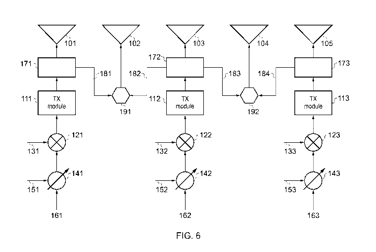
FIGURE 5 shows a typical set of radiation patterns for the array of Figure 4.
FIGURE 6 shows an antenna array of an embodiment of the present invention;
FIGURE 7 shows a typical set of radiation patterns for the array of Figure 6;
FIGURE 8 shows a first exemplary embodiment of the vectorial combiners shown
in Figure 6;
FIGURE 9 shows a second exemplary arrangement of the vectorial combiners
shown in Figure 6;
FIGURE 10 shows an example of an arrangement using digital IQ signals to the
Tx modules; and
FIGURE 11 shows an example of an arrangement configured to receive RF
signals.
DETAILED DESCRIPTION
[0025] For the purposes of the present disclosure, discussion will be focussed
on the
transmit (Tx) function of the array. It will be understood that corresponding
arrangements
may be made for a receiving (Rx) antenna or an antenna having both Tx and Rx
functions.
CA 02908826 2015-10-05
WO 2014/174298 PCT/GB2014/051277
7
[0026] In the conventional linear array of Figure 1, there are n radiating
elements
numbered 0 to n-1, each fed with currents having a linear phase progression
across the
array such that the total phase delay in the feed to the nth element is:
(Pn = -(n-1)cB
where 4)13 = (2-rrd/A) sin(00.
[0027] Here d is the uniform inter-element spacing, A is the wavelength and eg
is the beam
steering angle, measured from the direction normal to the line containing the
radiating
elements. To steer the main beam to a direction eg from the direction normal
to the array
in a clockwise direction, the current in each element must be delayed in phase
by (21-r/A)
sin(%) relative to its neighbour on its left. This results in the signals from
all the elements
arriving in phase in the desired direction. To steer the main beam in an
anticlockwise
direction, the phases of the currents are correspondingly advanced in phase.
[0028] The spacing d is chosen such that the outer sidelobes, known as grating
lobes,
remain below acceptable levels for the intended application. Reducing d
diminishes the
level of the grating lobes but may also reduce the maximum array gain.
[0029] Figure 2 shows a schematic representation of a known uniform broadside
active
phased array of five elements. The array comprises five radiating elements 101
to 105 fed
with radio signals by five transmitting modules 111 to 115. Radio signals are
applied by
input means 161 to 165 through phase shifting means 141 to 145 to mixers 121
to 125.
Following mixing with the local oscillator signals applied at input means 131
to 135, the
signal at the frequency to be transmitted is applied to the input of each
module 111 to 115.
The phase shifters 141 to 145 are each provided with control means 151 to 155
which
cause the phase shift applied to the radio signal to be varied under the
control of a digital
or analog control signal.
[0030] It will readily be appreciated that the circuit elements associated
with each radiating
element are similar in function.
[0031] Figure 3 shows the element currents and computed radiation patterns for
the array
of Figure 2 for beam steering angles of 0 , 10 and 20 .
[0032] Figure 4 shows a schematic representation of a five-element broadside
array fed
as two outer subarrays with elements 101, 102 and 104, 105 fed from power
dividers 161,
162 respectively. The power dividers 161, 162 and the central element 103 are
excited by
means of Tx modules 111, 112, 113. The arrangements for feeding the Tx modules
111,
112, 113 are similar to those shown in Figure 2, with radio signal input means
161, 162,
163, phase shifters 141, 142, 143, control means 151, 152, 153, mixers 121,
122, 123 and
local oscillator input means 131, 132 133. It will be seen that in this
arrangement only
CA 02908826 2015-10-05
WO 2014/174298 PCT/GB2014/051277
8
three Tx modules and associated hardware are required to drive the five-
element array,
but there is no means whereby the relative phase of the currents in elements
101 and 102
or the relative phase of the currents in elements 104 and 105 may be adjusted
other than
by choice of the lengths of the transmission lines by which they are connected
to their
respective power dividers 161, 162.
[0033] Figure 5 shows the element currents and computed radiation patterns for
the array
of Figure 4 for beam steering angles of 0 , 10 and 20 . It will be seen that
the radiation
patterns at a 100 steering angle are very similar to those of the full array
shown in Figure 3,
but at steering angles of 0 and 20 the sidelobe levels are significantly
higher and are
unacceptable for use in mobile radio networks in dense urban areas.
[0034] The radiation pattern F(8) of a broadside array of N antenna elements
is given by:
;a(Uagee.40.)
(1)
where..A4 and= ie dimction. o.f.. the
beam .whiett can be. =derived when 1..F(.0)1 oets maximum.
vnint= from
A.
t,* . __
2.md
(2)
=
.= salVSinkssssssss,ss, A4)
'2.7M
[0035] From equation (1) it can be seen that the phase of the second element
is the
average of the phases of the two adjacent elements (e.g. the first and the
third element)
providing the required linear progressive phase difference L B.
[0036] Applying this concept, a simple mathematical summation or averaging
device is
inserted between two phase shifting control elements as shown in Figure 6. The
expensive Tx modules, which include but are not restricted to mixers, PAs, pre-
PAs,
heatsinks, BPFs and tuning circuits for improved VSWR performance are not
required for
alternate elements.
[0037] Figure 6 shows a schematic representation of a five-element broadside
array
configured according to an embodiment of the present invention. In this
arrangement,
radio signals are applied by input means 161-163 through phase shifting means
141-143
provided with analog or digital control means 151-153 to mixers 121-123.
Following
mixing with the local oscillator signals applied at input means 131-133, the
signal at the
frequency to be transmitted is applied to the input of the modules 111-113.
CA 02908826 2015-10-05
WO 2014/174298 PCT/GB2014/051277
9
[0038] The outputs of the Tx modules 111-113 are each applied to the input of
power
dividers 171-173, whose function is to apply a defined fraction of the power
applied to
them to the vectorial combiners 191, 192 by way of interconnecting
transmission lines 181-
184 and the remainder of the input power to the radiating elements 101, 103,
105. Outputs
of the combiners 191 and 192 are fed to the radiating elements 102 and 104
respectively.
By suitable choice of the relative amplitudes of the output levels from each
Tx module 111-
113 and the choice of the division ratio of the power dividers 171-173, it is
possible to
achieve a suitable weighting of the element currents to achieve the required
degree of
sidelobe suppression.
[0039] The architecture of the arrangement of Figure 6 is similar to that of a
paired
element array (Figure 4) to reduce components and costs, but without the
performance
degradation. The vectorial combiner or averaging device has the same effect as
if a full
phase shifter, transmit module and mixer were in line with the radiating
element fed
thereby, as can be seen from Figure 7, which shows the element currents and
computed
radiation patterns for the array of Figure 6 for beam steering angles of 0 ,
100 and 20 .
[0040] Figure 8 shows an exemplary arrangement of each of the vectorial
combiners 191,
192. The function of each combiner is to combine the inputs of two radio
frequency
signals and to output a signal whose amplitude is the sum of the two inputs
and whose
phase is the mean of the phases of the two input signals.
[0041] In Figure 8 the input signals are applied via connecting means 181(183)
and
182(184) to the inputs of respective power dividers 201, 211 whose function is
to provide a
low-level sample signal to the phase detectors 203, 213 by way of connecting
means
201b, 211b. The signal to the second input of each of said phase detectors
203, 213 is
obtained via connecting means 214a, 214b from a reference oscillator 215 via a
power
splitter 214. The outputs of the phase detectors 203, 213, containing the
required phase
information, are fed to the control ports of tuneable phase shifters 202, 212
via connecting
means 203a, 213a. The other outputs of the power dividers 201, 211,
representing the
remainder of the input signals applied at 181(183) and 182(184) is passed to
the inputs of
respective phase shifters 202 and 212 by way of connections 201a, 212a. The
phase
shifters 202, 212 are adjusted in response to the input signals at their
control ports in such
a manner as to bring the two signals presented to the power combiner 204 via
connecting
means 202a, 212a in phase with one another before they are combined. The
output from
the power combiner 204 is delivered via connecting means 204a to a tuneable
phase
shifter 205 whose setting is controlled by the signal provided from the output
of the
operational amplifier 206 via the connecting means 206a. By these means the
phase
CA 02908826 2015-10-05
WO 2014/174298 PCT/GB2014/051277
shifter 205 is adjusted such that the phase of the output signal lies mid-way
between the
phases of the input signals at 181 and 182.
[0042] The combiner 192 is configured and operates in the same manner as the
combiner
191. It is connected to power dividers 172, 173 via connecting means 183, 184
and its
5 output drives radiating element 104.
[0043] The control lines 203a, 213a, 206a may carry signals in analog format,
or with
appropriate interfaces in an alternative embodiment, in digital format.
In a digital
implementation the operational amplifier 206 may be replaced by a simple
microprocessor.
[0044] In a further embodiment the reference signal fed to the power splitter
214 may be
10 derived from one of the input signals 161, 162 or 163.
[0045] Figure 9 shows a further embodiment in which a phase detector 203
having inputs
201b and 211b is connected to the sample ports of power dividers 201 and 211
respectively. The main output from power divider 201 is connected via
connecting means
201a to tuneable phase shifter 202 and thence by connecting means 202a to a
first input
of a power combiner 204. The main output of power divider 211 is connected
directly via
connecting means 211a to a second input of the power combiner 204. The output
control
signal from the phase detector 203 is applied to the control port of the
tuneable phase
shifter 202 by connecting means 203a. The phase shift applied by the tuneable
phase
shifter 202 is adjusted in response to the input control signal to ensure that
the inputs
202a, 211a to the power combiner 204 are in phase.
[0046] Connecting means 203b carries the output control signal from the phase
detector
203 to an input of an operational amplifier 212. The signal is scaled by the
amplifier 212
and applied to the control port of the tuneable phase shifter 205 by way of
connecting
means 206a. The phase of the tuneable phase shifter 205 is adjusted in
response to the
input control signal to a value equal to one half of the phase shift applied
by the phase
shifter 202. It will be understood that the total phase shifts associated with
the radio paths
from the inputs 181(183) and 182(184) to the input 204a of the tuneable phase
shifter 205
must be equal and must be such that the currents in the radiating element
102(104) are
cophased with those of the remaining elements of the complete array when the
applied
input signals at 181(183) and 182(184) are cophased.
[0047] Figure 10 shows an alternative arrangement to that of Figure 6,
configured for
operation with digital IQ radio signals. In such an arrangement, the Tx
modules 901, 902,
903 accept digital IQ input signals and modulate a radio frequency signal
which is output to
the power dividers 171, 172, 173. Phase shifters 941, 942, 943 operate on the
input IQ
data streams in such a way as to vary the phase of the radio frequency signal
at the output
CA 02908826 2015-10-05
WO 2014/174298 PCT/GB2014/051277
11
of the Tx modules 901-903 in response to a control signal applied via input
means 151,
152, 153. It will be understood that the said phase shifts may be realised by
digital means
within the Tx modules 901-903.
[0048] Figure 11 shows a receiving antenna array comprising three antenna
elements
301, 302, 303 connected to the inputs of three receiver (Rx) modules 304, 305,
306 whose
outputs are connected to mixers 307, 308, 309 providing received signal
outputs 310, 311,
312. In an exemplary implementation the control of the amplitudes and phases
of the
received signals is procured by varying the amplitude and phase of local
oscillator signals
applied to the mixers 307, 308, 309. Accordingly a local oscillator signal is
provided at
inputs 131, 132 to two phase shifters 141, 142, whose respective outputs are
connected to
the mixers 307, 308, 309 by means of power dividers 171, 172 and a combining
circuit 191
which may be configured in the manner shown in Figures 8 or 9.
[0049] Throughout the description and claims of this specification, the words
"comprise"
and "contain" and variations of them mean "including but not limited to", and
they are not
intended to (and do not) exclude other moieties, additives, components,
integers or steps.
Throughout the description and claims of this specification, the singular
encompasses the
plural unless the context otherwise requires. In particular, where the
indefinite article is
used, the specification is to be understood as contemplating plurality as well
as singularity,
unless the context requires otherwise.
[0050] Features, integers, characteristics, compounds, chemical moieties or
groups
described in conjunction with a particular aspect, embodiment or example of
the invention
are to be understood to be applicable to any other aspect, embodiment or
example
described herein unless incompatible therewith. All of the features disclosed
in this
specification (including any accompanying claims, abstract and drawings),
and/or all of the
steps of any method or process so disclosed, may be combined in any
combination,
except combinations where at least some of such features and/or steps are
mutually
exclusive. The invention is not restricted to the details of any foregoing
embodiments.
The invention extends to any novel one, or any novel combination, of the
features
disclosed in this specification (including any accompanying claims, abstract
and drawings),
or to any novel one, or any novel combination, of the steps of any method or
process so
disclosed.
[0051] The reader's attention is directed to all papers and documents which
are filed
concurrently with or previous to this specification in connection with this
application and
which are open to public inspection with this specification, and the contents
of all such
papers and documents are incorporated herein by reference.