Note : Les descriptions sont présentées dans la langue officielle dans laquelle elles ont été soumises.
CA 02915232 2015-12-11
WO 2015/023359
PCT/US2014/042792
Power Architecture for an Implantable Medical Device Having a
Non-Rechargeable Battery
CROSS-REFERENCE TO RELATED APPLICATIONS
[001] This international application claims priority to U.S. Application
Serial No.
13/966,510, filed August 14, 2013, which is incorporated herein by reference
in its entirety.
FIELD OF THE INVENTION
[002] The present invention relates generally to implantable medical devices,
and more
particularly to improved architectures for an implantable medical device
having a primary
battery.
BACKGROUND
[003] Implantable neurostimulator devices are devices that generate and
deliver electrical
stimuli to body nerves and tissues for the therapy of various biological
disorders, such as
pacemakers to treat cardiac arrhythmia, defibrillators to treat cardiac
fibrillation, cochlear
stimulators to treat deafness, retinal stimulators to treat blindness, muscle
stimulators to
produce coordinated limb movement, spinal cord stimulators to treat chronic
pain, cortical
and deep brain stimulators to treat motor and psychological disorders, and
other neural
stimulators to treat urinary incontinence, sleep apnea, shoulder subluxation,
etc. The
description that follows will generally focus on the use of the invention
within a Spinal Cord
Stimulation (SCS) system, such as that disclosed in U.S. Patent 6,516,227.
However, the
present invention may find applicability in any implantable medical device.
[004] As shown in Figures 1A and 1B, a SCS system typically includes an
Implantable Pulse
Generator (IPG) 100, which includes a biocompatible device case 30 formed of a
conductive
material such as titanium for example. The case 30 typically holds the
circuitry of the IPG
and a battery to provide power to the circuitry. Depending on the particular
needs and
circumstances of the patient who will be using the IPG, the battery can be
either rechargeable
or a non-rechargeable primary battery. The IPG 100 includes one or more
electrode arrays
(two such arrays 102 and 104 are shown), each containing several electrodes
106. The
electrodes 106 are carried on a flexible body 108, which also houses the
individual electrode
leads 112 and 114 coupled to each electrode. In the illustrated embodiment,
there are eight
1
CA 02915232 2015-12-11
WO 2015/023359
PCT/US2014/042792
electrodes on array 102, labeled El-Es, and eight electrodes on array 104,
labeled E9-E16,
although the number of arrays and electrodes is application specific and
therefore can vary.
The arrays 102, 104 couple to the IPG 100 using lead connectors 38a and 38b,
which are
fixed in a non-conductive header material 36, which can comprise an epoxy for
example.
[005] As shown in Figure 2, the IPG 100 typically includes an electronic
substrate assembly
including a printed circuit board (PCB) 16, along with various electronic
components 20,
such as microprocessors, integrated circuits, and capacitors mounted to the
PCB 16. Some of
these electronic components 20 are discussed further below. A telemetry coil
13 (more
generally, an antenna) is generally present in the IPG 100 to transmit/receive
data to/from an
external controller 80. The telemetry coil 13 is typically mounted within the
header 36 of the
IPG 100 as shown, and may be wrapped around a ferrite core 13'. In other
embodiments, the
telemetry coil 13 may be within the case 30. In an IPG having a rechargeable
battery, such as
the IPG 100, a charging coil 18 is also present for charging or recharging the
IPG's battery
using an external charger 82.
[006] As just noted, an external controller 80, such as a hand-held programmer
or a
clinician's programmer, is used to wirelessly send data to and receive data
from the IPG 100.
For example, the external controller 80 can send programming data to the IPG
100 to dictate
the therapy the IPG 100 will provide to the patient. Also, the external
controller 80 can act as
a receiver of data from the IPG 100, such as various data reporting on the
IPG's status. The
external controller 80, like the IPG 100, also contains a PCB 70 on which
electronic
components 72 are placed to control operation of the external controller 80. A
user interface
74 similar to that used for a computer, cell phone, or other hand held
electronic device, and
including touchable buttons and a display for example, allows a patient or
clinician to operate
the external controller 80. The communication of data to and from the external
controller 80
is enabled by a coil (antenna) 17, which communicates with coil 13 in the IPG
100.
[007] The external charger 82, also typically a hand-held device, is used to
wirelessly convey
power to the IPG 100, which power can be used to recharge the IPG's battery if
it is
rechargeable. The transfer of power from the external charger 82 is enabled by
a coil
(antenna) 17', which generates power received by coil 18 in the IPG 100. The
external
charger 82 is depicted as having a similar construction to the external
controller 80, but in
reality they will differ in accordance with their functionalities as one
skilled in the art will
appreciate.
[008] Figure 3 illustrates an architecture for an IPG 100 that uses a
rechargeable battery 26.
Shown with particular emphasis in Figure 3 are the various power supplies in
the IPG 100,
2
CA 02915232 2015-12-11
WO 2015/023359
PCT/US2014/042792
which are the focus of this disclosure and which are shown with thicker lines.
Only a few
other non-power supply signals are shown in Figure 3 to the extent they are
discussed below,
and such signals are shown with thinner lines. One skilled in the art will
appreciate that the
IPG 100 contains many such "regular" signal lines, which are not shown for
convenience.
[009] Rechargeable battery 26 typically comprises a Lithium ion polymer
battery, and
depending on its level of depletion can have a battery voltage, Vbat, of about
3.2 to 4.2 Volts.
The IPG 100 includes a battery interface circuit 32, which acts as an
intermediary between
the charging coil 18 and the rechargeable battery 26. The battery interface
circuit 32 contains
circuitry for rectifying power received at the charging coil 18 from the
external charger 82
(Fig. 2) and for charging the rechargeable battery 26 in a controlled fashion.
Power from the
rechargeable battery 26 is routed through controllable switching circuitry in
the battery
interface circuit 32 and supplied to the rest of the circuitry in the IPG 100
as voltage, Vbat'.
The magnitude of Vbat' is essentially the same as Vbat, minus a small voltage
drop that
occurs across the switching circuitry in the battery interface circuit 32.
Examples of battery
interface circuitry 32 can be found in U.S. Patent Application 61/509,701,
filed July 20, 2011.
[0010] The battery interface circuit 32 supplies the voltage Vbat' to various
circuit elements
in the IPG 100 via voltage regulators 40, 42, and 44. The regulators 40, 42,
and 44 are used
to regulate Vbat' to power supply voltages VDDA, VDDD, and VDDF appropriate to
power
the circuit elements to which they are connected, i.e., analog circuitry 50,
digital circuitry 52,
and memory 54 respectively. The regulators 40, 42, and 44 can comprise low
power, low
drop out linear regulators that use very little power, which is particularly
useful in a battery
powered implanted medical device as it conserves power. Linear regulators are
also
advantageous because they create less noise than switching regulators.
[0011] Although the magnitude of the power supply voltages VDDD, VDDA, VDDF
needed
for each of circuitries 50, 52, and 54 may be the same, each circuitry is
preferably supplied
power by its own voltage regulator. The analog circuitry 50 and the digital
circuitry 52
preferably have separate regulators 40 and 42 because the digital circuitry 52
creates noise on
VDDD as it switches, which noise could potentially affect the performance of
the analog
circuitry 50. Memory 50 preferably has its own regulator 44 because the memory
50 may
consume a large amount of current, which VDDF must supply. Additionally, VDDF
can be
shut down from time to time to save power.
[0012] Analog circuitry 50 contains a number of low voltage analog circuitry
elements within
the IPG 100 that are powered by power supply VDDA, including thermistors, band
gap
voltage references, oscillators and clocks, modulation and demodulation
circuitry that sends
3
CA 02915232 2015-12-11
WO 2015/023359
PCT/US2014/042792
data to and receives data from the tank circuitry 24 coupled to the telemetry
coil 13, analog
measurement and routing circuitry, and the like. VDDA in one example may
comprise 2.8
Volts.
[0013] Digital circuitry 52 comprises the digital circuits in the IPG 100 that
are powered by
power supply VDDD, including microcontroller 60 and timing circuitry 66. VDDD
in one
example may comprise 2.8 Volts. Digital circuitry 52 can be integrated, at
least in part, on a
single mixed-mode ASIC integrated circuit with at least some of the analog
circuitry 50, as
shown for example in U.S. Patent Publication 2008/0319497, or can be discrete
therefrom.
[0014] Memory 54, which is powered by power supply VDDF, can hold the
operating
software for the system (e.g., for the microcontroller 60), and can also act
as a free space to
store data, such as logged data to be reported to the external controller 80
for analysis and/or
feedback to the patient. Memory 54 can also store data transmitted from the
external
controller 80, such as the therapy setting referred to earlier, which data can
in turn be sent to
the microcontroller 60. Memory 54 may be any type of memory, such as Flash
EPROM,
random access memory (RAM), static RAM (SRAM), a hard drive, or the like.
However, to
ensure data retention even when power is lost, memory 54 often comprises a
Flash EPROM
memory. Because a Flash EPROM can require additional current to both program
and erase,
VDDF is typically provided by a higher-powered regulator 44, as mentioned
previously.
VDDF in one example may comprise 2.8 Volts.
[0015] Rechargeable battery 26 also provides the power necessary to send
therapeutic current
pulses through particular stimulating electrodes 106. This is done by
producing a compliance
voltage, V+, using a DC-DC converter 22. Converter 22, like regulators 40, 42,
and 44,
creates a voltage (V+) from Vbat', which is used to power one or more Digital-
to-Analog
Converters (DAC) 33 to produce the therapeutic current, lout. The compliance
voltage V+ in
effect comprises the power supply for the DAC(s) 33. The magnitude of the
therapeutic
current, lout, produced by the DAC(s) 33 is specified by digital signals 61.
lout is output to a
particular electrode 106 of the IPG 100, which may be selected, where it
passes through the
tissue, R 25, of the patient. (Another electrode 106' can provide a return
path, or reference,
for lout).
[0016] Because the therapeutic current can vary from time to time, the
compliance voltage
V+ necessary to produce this current can vary as well, and thus V+ can be
changed by the
converter 22. As explained in U.S. Patent Publication 2007/0097719, V+ monitor
and adjust
circuitry 19 can measure the voltage at the electrode 106 when the DAC 33 is
issuing the
therapeutic current, and can inform the converter 22 of a value for V+,
V+(opt), that is
4
CA 02915232 2015-12-11
WO 2015/023359
PCT/US2014/042792
optimal to supply that current. As explained in the '719 Publication, if V+ is
too low, the
DAC 33 will become "loaded" and unable to provide the desired current, Tout.
If V+ is too
high, the DAC 33 will be able to provide the desired current, but power will
be wasted: some
portion of the compliance voltage V+ will be dropped across the DAC 33 without
any useful
effect. As also disclosed in the '719 Publication, the converter 22 can
comprise a capacitor-
based change pump, an inductor-based step-up converter, or combination of
these. V+ may
be set by the converter 22 in one example from anywhere between 3 to 18 Volts.
[0017] Tank circuitry 24, which is coupled to the telemetry coil 13, is also
powered by Vbat'.
As shown in U.S. Patent Publication U.S. 2009/0069869 for example, tank
circuitry 24 can
comprise a tuning capacitor which operates in conjunction with the inductance
of the coil 13
to set its resonant frequency, and can further include transistors controlled
by modulation
circuitry (part of the analog circuitry 50) to switch the tank at the resonant
frequency when
the coil 13 is transmitting. When receiving data, the tank circuitry 24 is
instead coupled to
demodulation circuitry (which may also include part of the analog circuitry
50).
[0018] Although many IPGs use rechargeable batteries, there are situations in
which use of a
primary battery may be advantageous. A primary battery is one in which the
electrochemical
reaction is not reversible by passing a charging current therethrough, thus
rendering the
battery non-rechargeable. Primary batteries use up the materials in one or
both of their
electrodes and thus have a limited life span.
[0019] Primary batteries, however, are typically cheaper than rechargeable
batteries, and may
not suffer from the same reliability concerns. As such, the use of primary
batteries in a
medical implantable device is preferred when appropriate, for example, when
the expected
life of the primary battery would be expected to exceed the patient's life
expectancy, or in
situations where patients with physical or mental limitations would have
difficulty charging
the battery. Using a primary battery in an implantable medical device also
simplifies design,
in particular because a charging coil 18 is not necessary.
[0020] Figure 4 illustrates an architecture for an IPG 400 using a primary
battery 12, which
may for example be a Lithium CFx battery or SVO hybrid with CFx having a
voltage, Vbat,
of 1.2 to 3.2 Volts. As shown, many of the circuit elements and connections in
IPG 400 are
the same as those used in the rechargeable-battery IPG 100 of Figure 3. Such
similar aspects
are not again discussed.
[0021] A significant difference in the primary-battery architecture of Figure
4 is the use of a
boost converter 64 in lieu of battery interface circuit 32 to supply various
circuit blocks with
power from the primary battery 12. As its name implies, the boost converter 64
boosts the
CA 02915232 2015-12-11
WO 2015/023359
PCT/US2014/042792
battery voltage, Vbat, to a higher magnitude, Vbat+, suitable for use by the
circuit blocks to
which it is connected¨the regulators 40, 42, 44, the DC-DC converter 22, and
the tank
circuitry 24 coupled to the telemetry coil 13. Vbat+ in this example may be
3.2 V or so.
Such boosting is necessary because of the relatively low voltage of the
primary battery 12
relative to the rechargeable battery 26. If not boosted, Vbat would be too low
to enable the
regulators 40, 42, and 44 to produce power supply voltages VDDD, VDDA, and
VDDF of
the desired magnitudes (again, about 2.8V). Boost converter 64, like the DC-DC
converter
22, can comprise a capacitor-based change pump, an inductor-based step-up
converter, or
combination of these.
[0022] Unfortunately, using a boost converter 64 to boost the voltage supplied
to the circuit
elements in IPG 400 is inefficient, because such boosting itself takes power
from the primary
battery 12. Efficiency is particularly important in an implantable medical
device with a
primary battery, because the primary battery cannot be recharged.
[0023] Accordingly, implantable medical devices, and more specifically
implantable
stimulator devices, would benefit from improved architectures that use primary
batteries, and
embodiments of such a solution are provided herein.
BRIEF DESCRIPTION OF THE DRAWINGS
[0024] Figures lA and 1B show an implantable pulse generator (IPG), and the
manner in
which an electrode array is coupled to the IPG in accordance with the prior
art.
[0025] Figure 2 illustrates an IPG, an external controller, and an external
charger in
accordance with the prior art.
[0026] Figure 3 illustrates aspects of an IPG power architecture using a
rechargeable battery
in accordance with the prior art.
[0027] Figure 4 illustrates aspects of an IPG power architecture using a
primary battery in
accordance with the prior art.
[0028] Figure 5 illustrates aspects of an improved IPG power architecture
using a primary
battery.
[0029] Figure 6 illustrates aspects of an alternative improved IPG power
architecture using a
primary battery.
6
CA 02915232 2015-12-11
WO 2015/023359
PCT/US2014/042792
DETAILED DESCRIPTION
[0030] An improved architecture for an implantable medical device using a
primary battery is
disclosed which reduces the circumstances in which the voltage of the primary
battery is
boosted, and hence reduces the power draw in the implant. The architecture
includes a boost
converter for selectively boosting the voltage of the primary battery and for
supplying that
boosted voltage to certain of the circuit blocks, including digital circuitry,
analog circuitry,
and memory. However, the boost converter is only used to boost the battery
voltage when its
magnitude is below a threshold; if above the threshold, the battery voltage is
passed to the
circuit blocks without boosting. Additionally, some circuitry capable of
operation even at
low battery voltages¨including the telemetry tank circuitry and the compliance
voltage
generator¨receives the battery voltage directly without boosting, and without
regard to the
current magnitude of the battery voltage.
[0031] A modified improved architecture also includes a boost converter for
supplying a
boosted voltage to the circuit blocks, although in this modified improvement,
the boosted
voltage is always supplied to the circuit blocks regardless of the current
magnitude of the
battery voltage. This modification is useful when the battery voltage is
necessarily lower
than the minimal input power supply voltage necessary for the circuit blocks
to operate.
Circuitry capable of operation even at low battery voltages again receives the
battery voltage
directly without boosting.
[0032] Figure 5 illustrates the improved architecture for an IPG 500 using a
primary battery
12, which may be similar to primary batteries discussed earlier with reference
to Figure 4.
Once again, many of the circuit elements and connections in IPG 500 are the
same as those
used in the rechargeable-battery IPG 100 of Figure 3, and the primary-battery
IPG 400 of
Figure 4. Such similar aspects are not again discussed.
[0033] As with the primary-battery architecture of IPG 400 in Figure 4, IPG
500 comprises a
boost converter 64 to potentially boost the voltage of the primary battery 12,
Vbat, to a higher
voltage, Vbat+, necessary to power the various circuits. However, two
differences are
apparent.
[0034] First, the boost converter 64 is controlled by a switch 76, which
switch is set
depending on Vbat's relationship to a threshold, Vt. If Vbat is greater than
or equal to the
threshold, the switch 76 is set to route Vbat directly to as the input power
supply 88 to first
circuitry 81 which includes the regulators 40, 42, and 44 that produce the
power supply
voltages VDDD, VDDA, and VDDF for the analog circuitry 50, the digital
circuitry 52, and
the memory 54 respectively. If Vbat is less than Vt, the switch 76 routes Vbat
to the input 28
7
CA 02915232 2015-12-11
WO 2015/023359
PCT/US2014/042792
of the boost converter 64, thus allowing the boost converter 64 to supply a
higher voltage,
Vbat+, as the input power supply 88 to the first circuitry 81 and thus to the
regulators 40, 42,
and 44. Although not shown, the boost converter 64 can also be selectively
enabled only
when Vbat < Vt so that it does not attempt to boost when the switch 76 does
not route Vbat to
it. Such enable signal to the boost converter can comprise the same signal
used to control the
switch 76, or an inverse of that signal.
[0035] The value of the threshold Vt can be set in accordance with a minimum
voltage
required by the regulators 40, 42, and 44 to operate, and in accordance with
the expected
range of voltages of the primary battery, Vbat, which as noted earlier can
range from 1.2 to
3.2V. For example, if these regulators must produce power supplies VDDD, VDDA
and
VDDF equal to 2.8V, then Vt may be set to a slightly higher voltage of 2.9V.
Thus, if 2.9 <
Vbat < 3.2, switch 76 will send Vbat directly to the first circuitry 81
without boosting. The
regulators can then drop this voltage to appropriate power supply levels. If
1.2 < Vbat < 2.9,
then switch 76 will send Vbat to the boost converter 64, where it can be
boosted to Vbat+,
which again may comprise 3.2V or so. The regulators can again drop this
boosted voltage
Vbat+ to appropriate power supply levels. Using this scheme, and in
distinction to the
architecture of Figure 4, the battery voltage, Vbat, is not always boosted
before being sent to
the regulators, and instead is only boosted when Vbat has dropped below the
threshold.
Because voltage boosting requires power, selective enablement of the boost
converter 64 in
this fashion saves power in the IPG 500 compared to prior approaches.
[0036] Although not shown, determining the relevant magnitudes of Vbat and Vt
and
producing an appropriate control signal for the switch 76 can be accomplished
in several
different ways. Vbat can be digitized at an Analog-to-Digital (AID) converter
and digitally
compared to Vt at the digital circuitry 52 to issue an appropriate digital
control signal for the
switch 76. Alternatively, a comparator comprising part of analog circuitry 50
can receive
Vbat and Vt in analog form, which comparator can then issue the digital
control signal for the
switch 76. Switch 76 can comprise a single transistor, or more-complicated
switching
circuitry.
[0037] In a second difference with the primary-battery architecture of Figure
4, notice that
second circuitry 84¨including the telemetry tank circuitry 24 and the DC-DC
converter 22
that generates the compliance voltage, V+¨receives the battery voltage Vbat
directly without
boosting from the boost converter 64. This is in recognition that these
circuits can operate
satisfactorily even at very low levels for Vbat, and therefore that it is
unnecessary to expend
power boosting the input power supply 86 of those circuits to higher levels.
For example, the
8
CA 02915232 2015-12-11
WO 2015/023359
PCT/US2014/042792
DC-DC converter 22 already contains circuitry to boost its input voltage,
i.e., to V+ as
necessary to power the DAC(s) 33, and such boosting circuitry within the
converter 22 does
not require any particular magnitude of the input voltage to function. Tank
circuitry 24 can
also perform satisfactorily at low levels of Vbat. If Vbat drops to low
levels, the strength of
transmission of wireless signals from the coil 13 to the external controller
80 (Fig. 2) will be
reduced accordingly. However, even if wireless transmissions from the IPG 500
have a
reduced signal strength, they will still be capable of receipt at the external
controller 80,
although perhaps from a smaller distance. In any event, not powering the DC-DC
converter
22 and tank circuitry 24 from boost converter 64 once again reduces reliance
on the converter
64, which saves power in the IPG 500. Because boost converter 64 is operated
in only
particular, narrower circumstances, and is used only to power the regulators
40, 42, and 44,
the converter 64 need not supply an output Vbat+ with as high of a current
capacity.
[0038] The architecture of IPG 500 of Figure 5 results in significant power
savings when
compared with the architecture of IPG 400 of Figure 4, which as noted earlier
is important in
an implantable medical device that uses a primary, non-rechargeable battery.
The boost
converter 64 operates at an efficiency of about 70%, whereas the regulators
40, 42, and 44
operate at efficiencies at about 90% when reducing the input power supply 88
to form lower
power supply voltages VDDA, VDDD, and VDDF. Therefore, when Vbat > Vt, it is
more
efficient to allow the regulators to scale down the input power supply voltage
88 than to use
the boost converter 64 to provide this voltage.
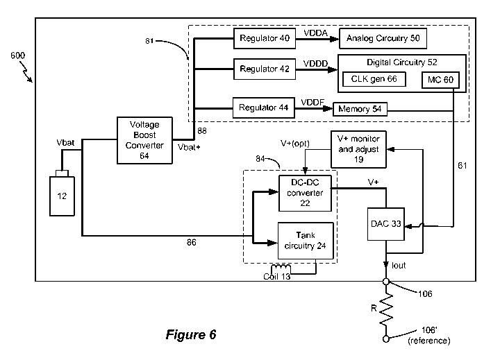
[0039] Figure 6 shows an alternative architecture for an IPG 600 having a
primary battery 12.
In this example, the switch 76 (Fig. 5) has been removed, and instead the
voltage boost
converter 64 always boosts the battery voltage Vbat to Vbat+ to power the
first circuitry 81
(regulators 40, 42, and 44; analog circuitry 50, the digital circuitry 52, and
memory 54) via
input power supply 88. As with the architecture of Figure 5, the second
circuitry 84
(telemetry tank circuitry 24; DC-DC converter 22 for generating the compliance
voltage V+)
receives the battery voltage Vbat directly without boosting from the boost
converter 64. This
architecture of Figure 6 is preferred when it is known that the primary
battery 12 is a lower-
voltage battery, and thus Vbat is too low to power first circuitry 81. For
example, if Vbat =
1.2V and is therefore less than the minimum input power supply voltage
necessary for the
regulators 40, 42, and 44 to operate, voltage boost converter 64 will need to
operate to boost
Vbat = 1.2V to Vbat+ > 2.9 V to provide an input power supply 88 suitable for
the regulators
40, 42, and 44 to produce the required values for VDDA, VDDD, and VDDF. By
contrast,
the second circuitry 84 is powered by and directly connected to the battery
12, which as
9
CA 02915232 2015-12-11
WO 2015/023359
PCT/US2014/042792
discussed with respect to Figure 5 is acceptable because these circuits can
operate sufficiently
at low levels and without boosting. Again, this saves power in the IPG 600,
even though the
boost converter 64 always operates to provide power to the regulators.
[0040] Although particular embodiments of the present invention have been
shown and
described, it should be understood that the above discussion is not intended
to limit the
present invention to these embodiments. It will be obvious to those skilled in
the art that
various changes and modifications may be made without departing from the
spirit and scope
of the present invention. Thus, the present invention is intended to cover
alternatives,
modifications, and equivalents that may fall within the spirit and scope of
the present
invention as defined by the claims.