Note : Les descriptions sont présentées dans la langue officielle dans laquelle elles ont été soumises.
CA 02919357 2016-01-26
Light Emitting diode (LED) display screen
Technical field of the invention
The present invention relates to the field of display screens, particularly to
a Light Emitting Diode (LED) display screen.
Background of the invention
Generally, an LED display screen is combined by splicing a plural number
of lamp beads in the related art, wherein a lamp bead product is mainly
encapsulated by a Surface Mounted Device (SMD), and a chip. However, an
SMD-encapsulated product and a chip-encapsulated product are size-limited,
wherein the existing minimum size of an SMD-encapsulated lamp bead can
only achieve 1.5mm*1.5mm while the existing minimum size of a
chip-encapsulated lamp bead can only achieve 0.8mm*0.8mm, thus the size of
an LED display screen is limited, the minimum dot pitch of an existing LED
display screen is limited to 1.6mm, and application of LED display screens in
the field of small size and high resolution LED display screens, e.g. in a
home
environment, is limited.
In a current stage, the sizes of conventional encapsulated lamp beads, i.e.
SMD-encapsulated and chip-encapsulated lamp beads are mainly limited by
an encapsulation structure. As shown in Fig. 1, a chip 102 is generally
arranged on a support 104 in a conventional encapsulation process while the
support 104 has a support function on one hand, and on the other hand,
serves as an electric connection medium to connect a chip electrode 106 and
a substrate 108, between Printed Circuit Boards (PCB) for example, wherein a
recessed structure is generally arranged at an upper end of the support 104 so
as to accommodate the chip 102 so that the chip 102 is fully fixed, thus the
support 104 is usually designed with a large size and reduction of the size of
an encapsulated lamp bead is limited.
CA 02919357 2016-01-26
Besides, an LED chip and a bonding pad are generally connected by a
metal wire according to a wire bonding technique of a conventional
encapsulated lamp bead, thus the quality of the lamp bead is directly affected
by the welding quality of the metal wire. While a dot pitch of an LED display
screen is reduced constantly, the conventional wire bonding technique also
limits the development of LED display screens. As shown in Fig. 1, a welded
part, i.e. the junction of a metal wire 110 and a chip 102 and the junction of
the
metal wire 110 and a bonding pad 112 on a support 104 are easily affected by
an external force or a temperature to cause a fracture in the wire bonding
technique of the conventional encapsulated lamp bead, thereby resulting in
deficient brightness of the lamp bead to further affect the display
performance
of an LED display screen.
At present, there is no effective solution yet for the foregoing problem.
Summary of the invention
An embodiment of the present invention provides an LED display screen,
so as to at least solve the technical problem in the related art that the
minimum
dot pitch of an LED display screen is excessively large due to a limited size
of
a support in a conventional encapsulated lamp bead.
An LED display screen is provided according to an aspect of the
embodiments of the present invention, including: an LED display screen
substrate, wherein the LED display screen substrate is arranged with a driving
circuit, an output end of the driving circuit includes: a first positive
electrode
and a first negative electrode and the first positive electrode and the first
negative electrode are located on a first surface of the LED display screen
substrate; an LED chip located on the first surface, wherein an input end of
the
LED chip includes: a second positive electrode and a second negative
electrode, the second positive electrode and the second negative electrode
are located on a second surface of the LED chip, and the second surface is
opposite to the first surface; a first jointing part and a second jointing
part,
2
CA 02919357 2016-01-26
wherein the first positive electrode is jointed to and electrically connected
to
the second positive electrode by the first jointing part, and the first
negative
electrode is jointed to and electrically connected to the second negative
electrode by the second jointing part.
Optionally, a plurality of said LED chips is arranged on the first surface of
the LED display screen substrate, wherein the distance between two adjacent
LED chips in the plurality of LED chips is set according to a preset dot pitch
of
the display screen.
Optionally, on the first surface, the plurality of LED chips is divided into a
plurality of LED chip groups having the same arrangement structure, wherein
each group in the plurality of LED chip groups includes: a first chip, a
second
chip and a third chip, wherein the first chip is configured to emit red
lights, the
second chip is configured to emit green lights and the third chip is
configured
to emit blue lights.
Optionally, the LED display screen further includes: an insulating rubber,
located between the first jointing part and the second jointing part and
implementing an insulating state between the first positive electrode and the
first negative electrode and between the second positive electrode and the
second negative electrode.
Optionally, the first jointing part and the second jointing part include: a
metal weldment, connected between the first positive electrode and the
second positive electrode, and/or between the first negative electrode and the
second negative electrode.
Optionally, the first jointing part and the second jointing part include: a
eutectic compound, connected between the first positive electrode and the
second positive electrode, and/or between the first negative electrode and the
second negative electrode.
Optionally, the first jointing part and/or the second jointing part
include/includes: a conductive silver paste, cured and connected between the
first positive electrode and the second positive electrode, and/or between the
3
CA 02919357 2016-01-26
first negative electrode and the second negative electrode.
Optionally, the first jointing part and/or the second jointing part
include/includes: an Anisotropic Conductive Paste (ACP), adhered between
the first positive electrode and the second positive electrode, and/or between
the first negative electrode and the second negative electrode.
Optionally, the ACP is adhered between the first positive electrode and the
second positive electrode, and between the first negative electrode and the
second negative electrode simultaneously and integrates the first jointing
part
and the second jointing part.
Optionally, the LED display screen further includes: a light transmitting
plate, located outside the LED chip, and jointed or adjacent with a third
surface
of the LED chip, wherein the third surface is opposite to the second surface.
In the embodiments of the present invention, since an installation method
of oppositely jointing an electrode of an LED chip and an electrode on an LED
display screen substrate is applied, a support as used in a conventional
encapsulation process is avoided so that the minimum dot pitch of an LED
display screen in the embodiments of the present invention is no longer
limited
by a size of the support, thus the technical problem in the related art that
the
minimum dot pitch of an LED display screen is excessively large due to a
limited size of a support in a conventional encapsulated lamp bead is solved
on the basis of ensuring relatively small sizes of a first jointing part and a
second jointing part between a chip electrode and a substrate electrode, and
the technical effect of reducing the minimum dot pitch of the LED display
screen is implemented. Further, use of a metal wire for electrically
connecting
an LED chip and the support in the conventional encapsulation process is
avoided in the embodiments of the present invention, thus eliminating the
influence of the welding quality on the performance of the LED display screen
to further achieve the technical effect of improving the reliability of the
LED
display screen.
4
CA 02919357 2016-01-26
Brief description of the drawings
The accompanying drawings illustrated herein are used for providing
further understanding to the present invention and constitute a part of the
application. The exemplary embodiments of the present invention and
illustration thereof are used for explaining the present invention, instead of
constituting improper limitation to the present invention. In the accompanying
drawings:
Fig. 1 is a schematic diagram of an LED lamp bead according to a related
encapsulation technology;
Fig. 2 is a schematic diagram of an optional LED display screen according
to an embodiment of the present invention;
Fig. 3 is a schematic diagram of another optional LED display screen
according to an embodiment of the present invention;
Fig. 4 is a schematic diagram of still another optional LED display screen
according to an embodiment of the present invention;
Fig. 5 is a schematic diagram of still another optional LED display screen
according to an embodiment of the present invention;
Fig. 6 (a) is a schematic diagram of still another optional LED display
screen according to an embodiment of the present invention;
Fig. 6 (b) is a schematic diagram of still another optional LED display
screen according to an embodiment of the present invention;
Fig. 7 is a schematic diagram of a manufacturing method of an optional
LED display screen according to an embodiment of the present invention;
Fig. 8 is a schematic diagram of a manufacturing method of another
optional LED display screen according to an embodiment of the present
invention;
Fig. 9 is a schematic diagram of still another optional LED display screen
according to an embodiment of the present invention;
Fig. 10 is a schematic diagram of an arrangement method of LED chips in
an optional LED display screen according to an embodiment of the present
CA 02919357 2016-01-26
invention;
Fig. 11 is a schematic diagram of an arrangement method of LED chips in
another optional LED display screen according to an embodiment of the
present invention;
Fig. 12 is a schematic diagram of a location relationship of LED chips in
an optional LED display screen according to an embodiment of the present
invention; and
Fig. 13 is a schematic diagram of still another optional LED display screen
according to an embodiment of the present invention.
Detailed description of the embodiments
The present invention will be expounded hereinafter with reference to the
accompanying drawings and in conjunction with the embodiments. It needs to
be noted that the embodiments in the application and the characteristics in
the
embodiments may be combined with each other if there is no conflict.
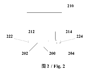
An embodiment of the present invention provides a preferred LED display
screen. As shown in Fig. 2, the LED display screen includes:
1) an LED display screen substrate 200, wherein the LED display screen
substrate 200 is arranged with a driving circuit, an output end of the driving
circuit includes: a first positive electrode 202 and a first negative
electrode 204
and the first positive electrode 202 and the first negative electrode 204 are
located on a first surface of the LED display screen substrate 200;
2) an LED chip 210 located on the first surface, wherein an input end of
the LED chip 210 includes: a second positive electrode 212 and a second
negative electrode 214, the second positive electrode 212 and the second
negative electrode 214 are located on a second surface of the LED chip 210,
and the second surface is opposite to the first surface;
3) a first jointing part 222 and a second jointing part 224, wherein the first
positive electrode 202 is jointed to and electrically connected to the second
positive electrode 212 by the first jointing part 222, and the first negative
6
CA 02919357 2016-01-26
electrode 204 is jointed to and electrically connected to the second negative
electrode 214 by the second jointing part 224.
The LED display screen substrate 200 in the LED display screen provided
according to the embodiment of the present invention may be arranged with
the driving circuit, wherein the driving circuit may be configured to generate
a
control voltage and/or a control current while the first positive electrode
202
and the first negative electrode 204 serving as output ends of the driving
circuit
may be configured to output the control voltage and/or the control current,
thus
the control voltage and/or the control current may be configured to control a
light emitting state of the LED chip 210.
In the embodiment of the present invention, a specific threshold range of
the control voltage and/or the control current may be set according to a
specification and/or a model of the LED chip 210 controlled by the control
voltage and/or the control current, thus the driving circuit configured to
generate the control voltage and/or the control current may be also provided
with various feasible corresponding forms and structures, which will not be
described repeatedly here in the embodiment of the present invention.
As shown in Fig. 2, in the embodiment of the present invention, the first
positive electrode 202 and the first negative electrodes 204 serving as the
output ends of the driving circuit may be located at the same side of the LED
display screen substrate 200, wherein a surface of the LED display screen
substrate 200 at the side is denoted by the first surface so as to facilitate
description. It needs to be noted that a positive electrode and a negative
electrode called in the embodiments of the present invention are only provided
to represent a corresponding connection relationship between an electric
connection end and a corresponding electric connection end thereof, but
should not be understood that there is any other unnecessary limitation. For
example, in same embodiments of the present invention, there may be a
plurality of first positive electrodes 202 on the first surface of the LED
display
screen substrate 200, and a corresponding first negative electrode 204 may be
7
CA 02919357 2016-01-26
a common end. The common end may manifest as a metal sheet having a
specific shape or a bonding pad connected by a conductor, and so on.
Optionally, there may be a plurality of options and combinations of the
shapes, structures or materials of the first positive electrode 202 and the
first
negative electrode 204 in the embodiment of the present invention. For
example, in terms of shapes, the first positive electrode 202 and the first
negative electrode 204 may be rectangular, or may be also circular or
semicircular, or in a shape formed by combining a circle and a rectangle; in
terms of materials, the first positive electrode 202 and the first negative
electrode 204 may be silver electrodes, or may be also metal materials
including copper, gold and so on, or other conductor materials; in terms of
structures, the first positive electrode 202 and the first negative electrode
204
are arranged with smooth surfaces fitted with the LED chip 210, or may be also
partly or wholly provided with a certain curvature, or may be further provided
with a preset texture or a structure including a convex or a groove and so on,
wherein the surfaces of the first positive electrode 202 and the first
negative
electrode 204 may be aligned with the LED display screen substrate 200, or
may be also provided with relatively evident convexes relative to the surface
of
the LED display screen substrate 200, or may be also arranged according to
the structure of an electrode of the LED chip 210. For example, the first
positive electrode 202 and the first negative electrode 204 may be provided
with different heights or thicknesses. Of course, the above are only some
examples, and the embodiments of the present invention do not make any
improper limitation to this.
On the other hand, the LED display screen substrate 200 in the
embodiment of the present invention may be generally a PCB. However, in
some embodiments of the present invention, the LED display screen substrate
200 may be also a ceramic circuit board, such as a porous ceramic circuit
board, a Low Temperature Co-fired Ceramic (LTCC) circuit board and so on, or
is designed by applying other feasible materials that may be used as a circuit
8
CA 02919357 2016-01-26
board or feasible processes, which is not limited by the embodiments of the
present invention. It is worth noting that the LED display screen substrate
200
in the embodiment of the present invention is not identically understood as an
LED substrate in a general sense, but should be understood as a feasible
substrate, including an LED substrate that may be used for assembling a LED
display screen.
As shown in Fig. 2, the LED display screen provided according to the
embodiment of the present invention may further include the LED chip 210
located on the first surface, wherein the second positive electrode 212 and
the
second negative electrode 214 serving as input ends of the LED chip 210 may
be located at the same side of the LED chip 210, wherein a surface of the LED
chip 210 at the side may be denoted by the second surface so as to facilitate
description,
wherein the second positive electrode 212 and the second negative
electrode 214 located on the second surface may represent a positive
electrode and a negative electrode of the LED chip 210, respectively, wherein
the LED chip 210 may be in different light emitting states according to
different
amplitudes of a control voltage and/or a control current inputted by the
second
positive electrode 212 and the second negative electrode 214, wherein it is
worth noting that the light emitting states of the LED chip 210 may be not
only
configured to represent on and off states of the LED chip 210, but also
configured to represent light emitting states of different brightness of the
LED
chip 210, and may be even configured to represent light emitting states of
different colors of the LED chip 210, which is not limited by the embodiments
of
the present invention.
Generally, the LED chip 210 may apply a related LED chip 210 product
directly in the embodiment of the present invention. Optionally, the LED chip
210 may be selected from various specifications and/or models. For example,
the LED chip may be a high power chip, or may be also a low power chip, may
be a single tube chip, or may be also a digital chip, a lattice chip, or a
chip for
9
CA 02919357 2016-01-26
decoration and illumination, and so on, which is not limited by the
embodiments of the present invention. Optionally, the sizes of the LED chip
210, and performance parameters including a positive onset voltage, a rated
current, a light emitting power and so on are also not specifically limited by
the
embodiments of the present invention. Optionally, each parameter of the LED
chip 210 may be configured according to a design requirement and an
application environment of the LED display screen. Of course, in some
embodiments of the present invention, the LED chip 210 may be also a
specific LED chip 210 product designed by a technician according to a related
product requirement, which is not limited by the embodiments of the present
invention.
As shown in Fig. 2, different from the related art, the side, i.e. the second
surface on the LED chip 210, where the second positive electrode 212 and the
second negative electrode 214 are distributed may be opposite to the first
surface of the LED display screen substrate 200 in the embodiment of the
present invention, but is not set back to back with the first surface in a
related
encapsulation process as shown in Fig. 1, thus a spatial structure formed by
the chip electrodes and the substrate electrodes is more compact compared
with the related encapsulation process, so that a connection structure between
the LED chip 210 and the LED display screen substrate 200 in the LED display
screen provided by the embodiment of the present invention may be provided
with a design of a smaller size.
Optionally, as shown in Fig. 2, the LED display screen in the embodiment
of the present invention may further include the first jointing part 222 and
the
second jointing part 224, wherein the first positive electrode 202 may be
jointed to and electrically connected to the second positive electrode 212 by
the first jointing part 222, and the first negative electrode 204 may be
jointed to
and electrically connected to the second negative electrode 214 by the second
jointing part 224.
In the scenario above, an electric connection relationship is formed
I()
CA 02919357 2016-01-26
between the substrate electrodes and the chip electrodes through the first
jointing part 222 and the second jointing part 224, thereby forming a
conduction circuit between the driving circuit and the LED chip 210 in the LED
display screen substrate 200 so as to control the LED chip 210 through the
control voltage/the control current outputted by the driving circuit to
further
implement a display function of the LED display screen.
Besides, as shown in Fig. 2, since an installation method of jointing the
electrodes of the chip 210 and the electrodes on the LED display screen
substrate 200 oppositely is applied in the embodiment of the present
invention,
a support as used in a conventional encapsulation process is avoided so that
the minimum dot pitch of the LED display screen in the embodiment of the
present invention is no longer limited by a size of the support, thus the
technical problem in the related art that the minimum dot pitch of an LED
display screen is excessively large due to a limited size of a support in a
conventional encapsulated lamp bead is solved on the basis of ensuring
relatively small sizes of a first jointing part 222 and a second jointing part
224
between a chip electrode and a substrate electrode, and the technical effect
of
reducing the minimum dot pitch of the LED display screen is implemented.
Further, use of a metal wire for electrically connecting an LED chip 210 and
the
support in the conventional encapsulation process is avoided in the
embodiment of the present invention, thus eliminating the influence of the
welding quality on the performance of the LED display screen to further
achieve the technical effect of improving the reliability of the LED display
screen.
Various specific embodiments of the first jointing part 222 and the second
jointing part 224 will be expounded below.
Referring to Fig. 3 to Fig. 5, and Fig. 6 (a) and Fig. 6 (b), as optional
embodiments of the embodiments of the present invention, the first jointing
part 222 and the second jointing part 224 may include at least one of the
followings:
11
CA 02919357 2016-01-26
1) A metal weldment 302, connected between the first positive electrode
202 and the second positive electrode 212, and/or between the first negative
electrode 204 and the second negative electrode 214.
2) A eutectic compound 402, connected between the first positive
electrode 202 and the second positive electrode 212, and/or between the first
negative electrode 204 and the second negative electrode 214.
3) A conductive silver paste 502, cured and connected between the first
positive electrode 202 and the second positive electrode 212, and/or between
the first negative electrode 204 and the second negative electrode 214.
4) An ACP 602, adhered between the first positive electrode 202 and the
second positive electrode 212, and/or between the first negative electrode 204
and the second negative electrode 214,
wherein a corresponding optional connection method, i.e. a chip fixing
method, between the chip electrodes and the substrate electrodes through the
first jointing part 222 and/or the second jointing part 224 in the first
implementation method may be a jointing method of planting a gold ball,
wherein as shown in Fig. 3, the metal weldment 302 may be a gold ball planted
on the first positive electrode 202 and the first negative electrode 204 of
the
LED display screen substrate 200 respectively, and the other side of the gold
ball is jointed with the second positive electrode 212 and the second negative
electrode 214 of the LED chip 210 respectively.
Optionally, a manufacturing process may be as shown in Fig. 7, including
the following steps:
Step 702: A gold ball is planted on the first positive electrode 202 and the
first negative electrode 204 of the LED display screen substrate 200,
respectively.
Step 704: The LED chip 210 is mounted on the first surface of the LED
display screen substrate 200, wherein the second surface of the LED chip 210
is opposite to the first surface, and the location of the second positive
electrode
212 is opposite to that of the gold ball planted on the first positive
electrode
12
CA 02919357 2016-01-26
202, and the location of the second negative electrode 214 is opposite to that
of the gold ball planted on the first negative electrode 204.
Step 706: The gold balls are subjected to fusion welding using ultrasonic
waves, and a pressure welding device welds the LED chip 210 on the LED
display screen substrate 200 in a pressing manner.
Of course, the above is only an example and is not limited by the
embodiments of the present invention. For example, the following step may be
also included before Step 704 in some embodiments of the present invention:
the horizontal locations of the gold balls on the first positive electrode 202
and
the first negative electrode 204 are calibrated. Besides, the following step
may
be also included before Step 706: the LED chip 210, corresponding bonding
pads of the first positive electrode 202 and the second positive electrode 212
on the LED display screen substrate 200, and/or the gold balls on the first
positive electrode 202 and the second positive electrode 212 are preheated,
and so on.
Besides, in some other embodiments of the present invention, the first
jointing part 222 and the second jointing part 224 may be also metal
weldments 302 formed by gold sheets or gold plates, but not the gold balls. In
addition, the metal weldments 302 may be also metals or alloy materials
besides gold, such as soldering tin, and the embodiments of the present
invention do not make any limitation thereto.
A corresponding chip fixing method of the second implementation method
may be a eutectic bonding method in an embodiment of the present invention,
wherein the first positive electrode 202 and the first negative electrode 204
of
the LED display screen substrate 200 may be respectively jointed with the
second positive electrode 212 and the second negative electrode 214 of the
LED chip 210 through the eutectic compound 402, as shown in Fig. 4.
Optionally, a manufacturing process may be as shown in Fig. 8, including
the following steps:
Step 802: Eutectic layers are covered on the first positive electrode 202
13
CA 02919357 2016-01-26
and the first negative electrode 204 of the LED chip 210.
Step 804: The LED ship 210 is mounted on the first surface of the LED
display screen substrate 200, wherein the second surface of the LED chip 210
is opposite to the first surface, and the location of the second positive
electrode
212 is opposite to that of the first positive electrode 202, and the location
of the
second negative electrode 214 is opposite to that of the first negative
electrode
204.
Step 806: The eutectic layers are heated at a preset temperature
condition.
Of course, the above is only an example, and is not limited by the
embodiments of the present invention. For example, some embodiments of the
present invention may also apply a jointing method of performing a eutectic
process assisted by a welding flux instead of applying a direct eutectic
process,
wherein an auxiliary welding flux may be arranged on the first positive
electrode 202 and the first negative electrode 204 of the LED display screen
substrate 200 in advance.
Besides, the eutectic layers in Step 802 may be selected from various
materials, and may be Au80Sn20 generally. However, the eutectic layers may
be also formed by compounds including CuSn or PbSn and so on in some
other embodiments of the present invention, which is not limited by the
embodiment of the present invention.
Similar to the second implementation method, the chip electrodes may be
aligned with the substrate electrodes first in third implementation method in
an
embodiment of the present invention, and the conductive silver paste 502
coated between the chip electrodes and the substrate electrodes is cured and
adhered between the first positive electrode 202 and the second positive
electrode 212 and between the first negative electrode 204 and the second
negative electrode 214 by means of heating and so on, as shown in Fig. 5,
which will not be described repeatedly in the embodiment of the present
invention.
14
CA 02919357 2016-01-26
A corresponding chip fixing method of the third implementation method
may be an ACP jointing method in an embodiment of the present invention,
wherein the first positive electrode 202 and the first negative electrode 204
of
the LED display screen substrate 200 may be jointed with the second positive
electrode 212 and the second negative electrode 214 of the LED chip 210
through the ACP 602, as shown in Fig. 6 (a).
Optionally, as shown in Fig. 6 (b), as a preferred implementation method,
the ACP 602 may be also adhered between the first positive electrode 202 and
the second positive electrode 212, and between the first negative electrode
204 and the second negative electrode 214 at the same time, and integrates
the first jointing part 222 and the second jointing part 224.
In Fig. 6 (b), different from the connection structure that the first jointing
part 222 and the second jointing part 224 are separated in the first
implementation method, the second implementation method and the third
implementation method, the ACP 602 may be formed to be integrally adhered
between the substrate electrodes and the chip electrodes, wherein as a
polymeric bonding agent, the anisotropy of the ACP may enable the ACP 602
to have better electrical conductivity in a direction vertical to the first
surface
and the second surface while the electrical conductivity in a direction
parallel to
the first surface and the second surface is worse, wherein the electrical
conductivity in the directions above may be implemented by a change of the
electrical conductivity with the directions due to insufficient contact
between
crystalline grains caused by a conductive filler material having a relatively
low
capacity. Since the ACP 602 may be integrally coated between the substrate
electrodes and the chip electrodes in the scenario above, alignment between
the first positive electrode 202 and the second positive electrode 212 and
between the first negative electrode 204 and the second negative electrode
214 is avoided, and a possible short circuit caused by mutual contact of the
first jointing part 222 and the second jointing part 224 in the first
implementation method to the third implementation method is avoided, thereby
CA 02919357 2016-01-26
achieving the technical effect of improving the reliability of the LED display
screen while reducing a requirement on the precision of a chip fixing device
and the manufacturing cost of the LED display screen.
Besides, it may be also seen from the foregoing description that besides
forming a connection loop between the LED display screen substrate 200 and
the LED chip 210, the first jointing part 222 and the second jointing part 224
in
the first implementation method to the fourth implementation method may also
fix the LED chip 210 on the LED display screen substrate 200, thereby also
implementing the technical effect of improving the reliability of the LED
display
screen.
Of course, provided as examples, the first implementation method to the
fourth implementation method are used for explaining the technical solutions
of
the present invention in more details, but should not be understood as forming
any limitation to the present invention. The technical solutions of the
present
invention may be also implemented by other methods, which will not be
described repeatedly here.
Optionally, as shown in Fig. 9, in the embodiment of the present invention,
the LED display screen may further include:
1) An insulating rubber 902, located between the first jointing part 222 and
the second jointing part 224 and implementing an insulating state between the
first positive electrode 202 and the first negative electrode 204 and between
the second positive electrode 212 and the second negative electrode 214.
As described above, in the first implementation method to the third
implementation method, the mutual contact between the first jointing part 222
and the second jointing part 224 may cause a short circuit of the driving
circuit
which is located on the LED display screen substrate 200 to drive the LED chip
210. As shown in Fig. 9, the insulating rubber 902 may be also filled between
the first jointing part 222 and the second jointing part 224 according to the
LED
display screen in the embodiment of the present invention, so as to at least
solve this problem, thereby solving the problem of the short circuit and
16
CA 02919357 2016-01-26
implementing the technical effect of improving the reliability of the LED
display
screen.
Optionally, the insulating rubber 902 may have various options, such as
epoxy resin and so on. It is worth noting that the insulating rubber 902 may
be
in a liquid state, and may be also in a solid state or a mixture of a liquid
and a
solid, which is not limited by the embodiments of the present invention.
By means of the embodiments above, the embodiments of the present
invention have elaborated a structure taking the chip as the smallest unit in
the
LED display screen. Optionally, the embodiments of the present invention will
expound an arrangement structure of LED chips 210 on the LED display
screen by means of the following embodiments,
wherein as shown in Fig. 10, a plurality of said LED chips 210 may be
optionally arranged on the first surface of the LED display screen substrate
200, wherein the distance between two adjacent LED chips in the plurality of
LED chips 210 may be set according to a preset dot pitch of the display
screen.
As shown in Fig. 10, the plurality of LED chips 210 may be generally
aligned regularly by means of a rectangular lattice in an embodiment of the
present invention. However, it does not mean that an arrangement method of
the LED chips 210 is limited by the embodiment of the present invention. For
example, the plurality of LED chips 210 may be also arranged in other ways.
For example, a method of arranging the chips in a slanting and intersecting
manner may be applied, as shown in Fig. 11. Besides, the LED chips 210 may
be also arranged along a preset pattern, which is not limited by the
embodiment of the present invention.
Optionally, the distance between two adjacent LED chips in the plurality of
LED chips 210 may be set according to a size of the chips and a design
requirement, such as the minimum dot pitch, of the LED display screen in the
embodiment of the present invention. For example, as shown by Fig. 12, in the
case that the shapes of light emitting surfaces of the LED chips 210 are
17
CA 02919357 2016-01-26
squares, the distance S between two adjacent LED chips 210 may be set
according to the following formula:
S=P-D, where S is provided to represent the distance between the chips,
P is provided to represent a preset minimum dot pitch and D is provided to
represent a side length of the squares serving as the outlines of the light
emitting surfaces of the chips.
On the other hand, an arrangement method of the LED chips 210 for an
LED display screen having a design requirement of color display may be
further set according to the design requirement, an imaging resolution and so
on in some embodiments of the present invention. For example, as an optional
embodiment of the present invention, on the first surface of the LED display
screen substrate 200, the plurality of LED chips 210 are divided into a
plurality
of LED chip 210 groups having the same arrangement structure, wherein each
of the plurality of LED chip 210 groups includes: a first chip, a second chip
and
a third chip, wherein the first chip is configured to emit red lights, the
second
chip is configured to emit green lights and the third chip is configured to
emit
blue lights.
In the scenario above, lights of three colors, i.e. red lights, green lights
and
blue lights of different proportions may be synthesized, according to the
principles of the three primary colors, into lights of other colors
recognizable by
human eyes, thereby the driving circuit may provide an adjustable control
voltage and/or control current to the first chip, the second chip and the
third
chip so as to control the color and brightness of the LED display screen.
Optionally, as shown in Fig. 13, the LED display screen may further
include the followings in an embodiment of the present invention.
1) A light transmitting plate 1302, located outside the LED chip 210, and
jointed or adjacent with a third surface of the LED chip 210, wherein the
third
surface is opposite to the second surface,
wherein the light transmitting plate 1302 may be configured to
encapsulate and protect a display side of the LED display screen, wherein the
18
CA 02919357 2016-01-26
light transmittance of the light transmitting plate 1302 may be set according
to
a design requirement. Besides, the embodiments of the present invention
make no limitation to a specific material and a shape of the light
transmitting
plate 1302.
The present invention provides the foregoing preferred embodiments to
further explain the present invention, but it is worth noting that the
foregoing
preferred embodiments only serve to better describe the present invention, but
do not constitute improper limitation to the present invention.
It may be seen from the foregoing description that the present invention
has implemented the following technical effect.
1) An installation method of directly jointing an electrode of an LED chip
210 and an electrode on an LED display screen substrate 200 is applied,
thereby avoiding the dependency on a support in a conventional encapsulation
process so that the minimum dot pitch of an LED display screen in the
embodiments of the present invention is no longer limited by a size of the
support, and achieving the technical effect of reducing the minimum dot pitch
of the LED display screen.
2) Use of a metal wire for electrically connecting an LED chip 210 and the
support in the conventional encapsulation process is avoided, thus eliminating
the influence of the welding quality on the performance of the LED display
screen to further achieve the technical effect of improving the reliability of
the
LED display screen.
The above are only preferred embodiments of the present invention, but
are not used for limiting the present invention. For those skilled in the art,
the
present invention may have various modifications and changes.
19
CA 02919357 2016-01-26
Industrial applicability
The embodiments of the present invention apply an installation method of
directly jointing an electrode of an LED chip and an electrode on an LED
display screen substrate, thereby avoiding the dependency on a support in a
conventional encapsulation process so that the minimum dot pitch of an LED
display screen in the embodiments of the present invention is no longer
limited
by a size of the support, and achieving the technical effect of reducing the
minimum dot pitch of the LED display screen. Further, use of a metal wire for
electrically connecting an LED chip and the support in the conventional
encapsulation process is avoided in the embodiments of the present invention,
thus eliminating the influence of the welding quality on the performance of
the
LED display screen to further achieve the technical effect of improving the
reliability of the LED display screen.