Note : Les descriptions sont présentées dans la langue officielle dans laquelle elles ont été soumises.
CA 02921290 2016-02-12
WO 2015/022414 PCT/EP2014/067457
1
RADIAL P-N JUNCTION NANOWIRE SOLAR CELLS
FIELD OF THE TECHNOLOGY
[0001] The present disclosure relates to photovoltaic devices, in particular
nanowire solar cells with radial p-n junctions for high solar cell
efficiencies.
BACKGROUND
[0002] Photovoltaic devices typically employ a planar thin-film
structure,
wherein a negatively doped (n-type) material is stacked on top of a positively
doped (p-type) material or a positively doped (p-type) material is stacked on
top
of a negatively doped (n-type) material. In these planar photovoltaic devices,
the light absorbing layer needs to be thick enough to effectively absorb
impinging photons with energies larger than the bandgap energy of the light
absorbing material. However, when the light absorbing layer in a planar
structure is made thicker this compromises the effective collection of the
photo-
generated carriers as the thickness of the light absorbing layer may be larger
than the diffusion length of the minority carriers. Therefore the design of
typical
planar photovoltaic devices leads to a compromise between the thickness of the
light absorbing layer for efficient light absorption and the effectiveness of
carrier
collection, thereby imposing limits on the efficiencies of these devices.
[0003] For example, typical thin-film GaAs solar cells require a light
absorbing
layer several microns thick to effectively absorb photons with energies higher
than its bandgap energy, but as the diffusion length of the minority carriers
is
typically only a few hundreds nanometres, many of the photo-generated carriers
cannot be collected.
[0004] Rather than using planar p-n junctions in photovoltaic devices, radial
p-n
junctions are being investigated. In these structures, a long central p-type
core
extends out of a substrate and an n-type shell is wrapped around the core. In
alternative configurations, the core is of an n-type material, while the shell
is
formed of a p-type material. Using this structure, one of the two photo-
generated carrier types is collected in the shell orthogonally to the light
CA 02921290 2016-02-12
WO 2015/022414 PCT/EP2014/067457
2
absorption along the length of the core.
Unlike in planar p-n junctions,
increasing the length of the core to improve light absorption does not
increase
the distance the carriers need to travel before being collected, and therefore
does not lead to the trade-off in light absorption and carrier collection
found in
typical planar devices.
[0005] Recent developments in the fabrication of nanowires extending out of
substrates have made it possible to manufacture radial p-n junction
photovoltaic
devices. However, the efficiencies that have been achieved with these radial
p-n junctions have been substantially less than corresponding planar devices,
achieving solar cell efficiencies of less than 10% under one-sun AM1.5G solar
spectrum illumination.
[0006] It is desirable for single-junction photovoltaic devices to achieve
solar
cell efficiencies as close to the Shockley-Queisser limit of -33.5% as
possible,
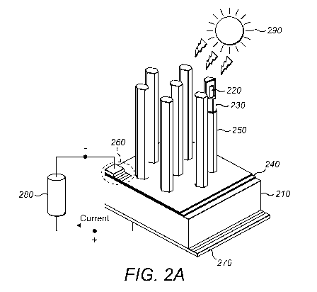
or even exceeding the limit, as higher solar cell efficiencies result in more
solar
energy collected per square metre of solar panel, leading to smaller
footprints
and potentially cheaper installations.
SUMMARY
[0007] In one embodiment, the present disclosure provides a photovoltaic
device comprising at least one nanowire structure fixed to a substrate,
wherein
each of the at least one nanowire structures comprise: a heavily doped p-type
core having a proximal end fixed to the substrate and a distal end extending
away from the substrate; and an n-type shell around the p-type core.
[0008] Nanowires with p-type cores and n-type shells allow for improved
carrier
collection compared to planar photovoltaic devices, resulting in potentially
improved solar cell efficiencies. While in planar photovoltaic devices the
solar
cell efficiencies are lowered with an increase in p-type doping, it has been
found
that by heavily doping the p-type layer nanowire core leads to substantial
improvements in solar cell efficiency.
CA 02921290 2016-02-12
WO 2015/022414 PCT/EP2014/067457
3
[0009] In some example embodiments the p-type core and the n-type shell are
III-V compounds.
[0010] In some example embodiments the p-type core is formed of GaAs and
the n-type shell is formed of AlxGai_xAs. GaAs compounds are particularly
suited for photovoltaic devices, as the bandgap energy of around 1.4eV allows
for high solar cell efficiencies in accordance with the Shockley¨Queisser
model.
[0011] In some example embodiments x (the Al mole fraction) has a value less
than or equal to 0.2. An Al mole fraction of 0.2 may minimise surface
recombination and the energy barrier in the conduction band at the interface
between the nanowire core and shell.
[0012] In some example embodiments the p-type core is sufficiently heavily
doped to at least one of: maximise quasi-Fermi level energy splitting,
maximise
a built-in electric field of the nanowire structure, extend an absorption
spectrum
of the nanowire structure, and maximise one or more of diffraction and
reflection of sunlight inwardly in the core.
Maximising diffraction and/or
reflection inwardly in the core may reduce optical reflection, enhance optical
confinement as well as maximise photon recycling.
[0013] In some example embodiments the doping density of the p-type core is
greater than 1018 cm-3 and preferably 1019 cm-3.
[0014] In some example embodiments the n-type shell is lightly doped. Lightly
doping the n-type nanowire shell may minimise the carrier loss due to carrier-
carrier scatterings, thereby maximising carrier collection efficiency and
solar
power conversion efficiency. Furthermore, lightly doping the n-type shell may
maximise the depletion region in the shell to minimise carrier recombination
in
the shell, hence maximising carrier collection efficiency and solar power
conversion efficiency.
[0015] In some example embodiments the doping density of the n-type shell is
less than 1017 cm-3 and preferably around 1016 cm-3.
CA 02921290 2016-02-12
WO 2015/022414 PCT/EP2014/067457
4
[0016] In some example embodiments the doping density of the p-type core is
greater than or equal to 1016 cm-3, and less than 1018 cm-3.
[0017] In some example embodiments the n-type shell is sufficiently thin to
minimise carrier recombination in the n-type shell. Furthermore, thin lightly-
doped shell may enable the collection of high-energy or hot electrons, hence
making it possible to achieve ultra-high solar power conversion efficiencies.
[0018] In some example embodiments the n-type shell has a thickness of
between 20nm and 50nm, and preferably 40nm.
[0019] In some example embodiments the diameter of the p-type core is
sufficiently large to maximise spectrum overlap between an incoming solar
spectrum and optical propagation modes of the nanowire . The diameter of the
p-type core may also be sufficiently large to achieve a good balance between
carrier collection and the amount of spectrum overlap between an incoming
solar spectrum and optical propagation modes of the nanowire.
[0020] In some example embodiments the diameter of the p-type core is greater
than 300nm, and preferably 400nm.
[0021] In some example embodiments the length of the nanowire is sufficiently
large to absorb deep-penetrating spectral components of an incoming solar
spectrum. The length of the nanowire may be restricted to avoid the
detrimental
effects of severe hole pile-up.
[0022] In some example embodiments the length of the nanowire is between
5pm and 7pm, and preferably 6pm.
[0023] In some example embodiments the substrate comprises silicon.
[0024] In some example embodiments the substrate comprises a graphitic layer
(such as graphene or modified graphene).
Graphitic layers are highly
CA 02921290 2016-02-12
WO 2015/022414 PCT/EP2014/067457
conductive, so may improve the solar power conversion efficiency and minimise
carrier losses.
[0025] In some example embodiments the distal end of the nanowire comprises
5 an anti-reflection coating.
[0026] In some example embodiments each of the at least one nanowire
structures are coated in a transparent conductive oxide (TCO).
[0027] In some example embodiments, a planar TCO contact lies above the at
least one nanowire structures.
[0028] In some example embodiments, an insulating polymer is disposed
between the planar TCO contact and the at least one nanowire structures.
[0029] In some example embodiments the p-type core has a radius greater than
300nm (preferably 400nm) and is formed of GaAs with a doping density greater
than 1018 cm-3 (preferably 1019 cm-3), the n-type shell has a thickness of
less
than 50nm (preferably 40nm) and is formed of A102Ga08As with a doping density
less than 1017 cm-3 (preferably 1016 cm-3), and the nanowire structure has a
length of between 5pm and 7pm, and preferably around 6pm. This combination
of material parameters and nanowire dimensions may lead to high solar cell
efficiencies of above 20%, and preferably above 30%.
[0030] In another embodiment, the present disclosure provides a method of
fabricating a photovoltaic device comprising at least one nanowire grown on a
substrate, the method comprising: growing a nanowire comprising a heavily
doped p-type core having a proximal end fixed to the substrate and a distal
end
extending away from the substrate, and an n-type shell around the p-type core.
[0031] In another embodiment, the present disclosure provides a solar cell
comprising plurality of the photovoltaic devices descried in the embodiments
above, wherein the plurality of photovoltaic devices are arranged in an array
with
a packing percentage of greater than 8%, preferably greater than 20%, and
CA 02921290 2016-02-12
WO 2015/022414 PCT/EP2014/067457
6
more preferably between 50 and 55%. By arranging an array of tightly packed
photovoltaic devices in a solar cell, the light trapping is improved, thereby
increasing the solar efficiency.
[0032] In another embodiment, the present disclosure provides a photovoltaic
device comprising at least one nanowire structure fixed to a substrate,
wherein
each of the at least one nanowire structures comprise: a planar TCO contact
above the at least one nanowire structures, wherein insulating polymer is
disposed between the planar TCO contact and the at least one nanowire
structures; a p-type core having a proximal end fixed to the substrate and a
distal end extending away from the substrate; and an n-type shell around the p-
type core.
BRIEF DESCRIPTION OF DRAWINGS
[0033] Examples of the present proposed approach will now be described in
detail with reference to the accompanying drawings, in which:
[0034] Figure 1 is a cross section of a single core-shell nanowire solar cell
on a
substrate;
[0035] Figures 2A and 2B are schematic diagrams illustrating solar cells made
out from an array of core-shell nanowires on a substrate;
[0036] Figure 3 shows a three-layer slab illustrating a computational method
used for determining optimum parameters of a nanowire;
[0037] Figure 4 shows energy band diagrams in short-circuit condition for a
range of p-type nanowire core doping densities;
[0038] Figure 5 is a graph showing the short-circuit current density and open-
circuit voltage as a function of the density of p-type nanowire core doping;
[0039] Figure 6 shows electric-field profiles in short-circuit condition for a
range
of p-type nanowire core doping densities;
CA 02921290 2016-02-12
WO 2015/022414 PCT/EP2014/067457
7
[0040] Figures 7 shows energy band diagrams in short-circuit condition for a
range of n-type nanowire shell doping densities;
[0041] Figure 8 is a graph showing the short-circuit current density and open-
circuit voltage as a function of the density of n-type nanowire shell doping;
[0042] Figure 9 shows electric-field profiles in short-circuit condition for a
range
of n-type nanowire shell doping densities;
[0043] Figure 10 is a chart showing solar cell efficiencies of a nanowire as a
function of p-type nanowire core doping density and n-type nanowire shell
doping density;
[0044] Figure 11 shows energy band diagrams in short-circuit condition for a
range of Al nanowire shell mole fractions;
[0045] Figure 12 shows electric-field profiles in short-circuit condition for
a
range of Al nanowire shell mole fractions;
[0046] Figure 13 is a graph showing the short-circuit current density and open-
circuit voltage as a function of Al nanowire shell mole fraction;
[0047] Figure 14 is a graph showing the solar cell efficiency as a function of
Al
nanowire shell mole fraction;
[0048] Figure 15 is a graph showing solar cell efficiency as a function of p-
type
core nanowire diameter for a range of nanowire lengths;
[0049] Figures 16 is a graph showing solar cell efficiency as a function of
nanowire lengths;
[0050] Figure 17 shows profiles of hole current densities along the length of
a
nanowire for a range of nanowire lengths; and
[0051] Figure 18 is a graph showing solar cell efficiency as a function of
shell
thickness with different TCO contact types;
CA 02921290 2016-02-12
WO 2015/022414 PCT/EP2014/067457
8
[0052] Figure 19 is a graph showing the J-V characteristics (relationship
between effective current density and voltage) of nanowires with different TCO
contact types in optimal conditions;
[0053] Figure 20 is a graph showing the J-V characteristics of nanowires with
different TCO contact types in ideal theoretical conditions;
[0054] Figure 21 shows energy band diagrams for different TCO contact types
in optimal conditions;
[0055] Figure 22 shows the carrier densities of profiles of nanowires with
different TCO contact types in optimal conditions;
[0056] Figure 23 shows the recombination rates of profiles of nanowires with
different TCO contact types in optimal conditions;
[0057] Figure 24 is a graph showing how solar cell efficiency of a nanowire
array is affected by the nanowire packing percentage of the array;
[0058] Figure 25 is a graph showing the J-V characteristics, solar cell
efficiency,
open-circuit voltage and fill factor of a nanowire array over a range of solar
ray
zenith angles of incidence; and
[0059] Figure 26 is a graph showing the J-V characteristics, solar cell
efficiency,
open-circuit voltage and fill factor of a nanowire array over a range of solar
ray
azimuth angles of incidence.
DETAILED DESCRIPTION
[0060] Reference will now be made to Figure 1 which shows a cross section of
an example nanowire structure. A p-type core 120 may be grown on a substrate
110 through a catalyst-free or catalyst-assisted process, for example, or may
be
fabricated by some other means that ensure that a distal end is fixed to the
substrate 110 while a distal end extends away from the substrate 110. The p-
type core may be a III-V compound, such as GaAs (gallium arsenide), as its
bandgap energy of around 1.4eV makes it suitable for achieving maximum solar
CA 02921290 2016-02-12
WO 2015/022414 PCT/EP2014/067457
9
cell efficiencies in the Shockley¨Queisser model. The substrate 110 may be a
p-type substrate to allow carriers to flow through from the p-type core.
[0061] The substrate 110 may by p-type silicon, for example, or any other
semiconductor. The substrate 110 may include a high electrical conductive
layer like a graphitic layer. The substrate may comprise a combination of
layers,
such as a silicon base with a thin graphitic layer on top, or even a graphitic
layer
on top of an insulating layer like glass. It would be clear to the skilled
person
what choice of substrate would be appropriate for allowing the core-shell
nanowires to grow from the substrate and remain fixed, while still allowing
for
the transport of generated charge carriers.
[0062] An n-type shell 130 is formed around the p-type core 120. The n-type
shell may be grown around the p-type core using a catalyst-free or catalyst-
assisted process as well, or by some other means. The n-type shell may be a
III-V compound such as AlxGai_xAs, where 'x' is the Al molar fraction.
[0063] The n-type shell 130 may be electrically insulated from the substrate
110 by having an insulating layer 140 between the shell 130 and substrate 110.
This insulating layer may be Si02, for example, and may be deposited on the
substrate prior to growing the p-type core and n-type shell.
[0064] To form an electric contact to the n-type shell 130, the device may
have
either a conformal contact or planar top contact made of either a transparent
conductive oxide (TCO) 150 or graphitic layer deposited on top.
[0065] To connect an electric load to the device, metal contacts may be
deposited on the top 160 and bottom 170 of the device, such that the top metal
contact 160 is in contact with the TCO layer 150 or graphitic layer, and
therefore
the n-type shell, and the bottom metal contact 170 is in contact with the p-
type
substrate 110, and therefore the p-type core 120.
[0066] Figure 2A shows a schematic diagram of an array of nanowires
arranged on a substrate 210. One nanowire is illustrated to show its interior,
CA 02921290 2016-02-12
WO 2015/022414 PCT/EP2014/067457
with a p-type core 220 at its centre extending away from the substrate 210,
the
p-type core 220 having an n-type shell 230 around it, and the whole nanowire
coated in the TCO 250 layer. Figure 2 shows that between the substrate 210
and the n-type shell 230, there may be an insulating layer 240 such as Si02. A
5 top metal contact 260 is connected to the negative terminal of an
electrical load
280, while the bottom contact 270 is connected to the positive terminal of an
electric load 280.
[0067] When light 290, typically with AM1.5G solar spectrum, is incident on
the
10 nanowire array, carriers are generated at each of the nanowires and
current
flows through the electric load 280.
[0068] Figure 2B shows a schematic diagram of an alternative embodiment to
that illustrated in Figure 2A. Similar to Figure 2A, one nanowire is
illustrated to
show its interior, with a p-type core 220 at its centre extending away from
the
substrate 210, the p-type core 220 having an n-type shell 230 around it.
Between the substrate 210 and the n-type shell 230, there may be an insulating
layer 240 such as Si02, and a bottom contact 270 is disposed under the
substrate 210. While Figure 2A illustrates a conformal TCO layer coating each
individual nanowire structure, the embodiment illustrated in Figure 2B has a
planar TCO contact 256 covering the array of nanowires, and the top metal
contact 260 is in connection with the planar TCO contact 256. The planar TCO
contact 256 may be supported by a transparent layer, preferably an insulating
polymer 255 that substantially surrounds each of the nanowire structures and
fills the gaps between the nanowire structures to effectively concentrate and
confine sunlight in the nanowires for maximal sunlight absorption and photon
recycling, hence maximising solar power conversion efficiency.
[0069] In some example embodiments, the nanowire is substantially cylindrical
with a cylindrical core and a cylindrical shell around it. The nanowire may be
substantially prism-shaped with an n-sided polygonal base, such as a hexagon,
at the proximal end of the prism and in contact with the substrate and the
other
face at the distal end extending out away from the substrate. In other example
embodiments, the nanowire is substantially conical, with the base at the
CA 02921290 2016-02-12
WO 2015/022414 PCT/EP2014/067457
11
proximal end near the substrate and the vertex at the distal end away from the
substrate. In some example embodiments there is a heavily n-doped cap in
between the n-type shell and the TCO or graphitic layer.
[0070] The physics involved in radial p-n junctions is different to that of
established planar p-n junction photovoltaic devices. Therefore, when
designing
an efficient radial p-n junction, well-known assumptions, design
considerations
and prejudices associated with planar p-n junctions need to be challenged in
order to achieve maximum solar cell efficiency. Therefore, when studying the
device physics of a novel radial p-n junction, new computational methods and
considerations need to be made.
[0071] In p-n junction devices, minority carrier transport may be an important
consideration as it can control the majority carrier transport. Therefore,
when
designing a radial p-n junction, attention should be paid to the transport of
minority carriers in order to obtain desirable voltage-current
characteristics.
[0072] Unlike planar p-n junction solar cells, the boundaries of radial p-n
junction nanowire solar cells are essentially three dimensional. Therefore,
although more computational expensive, in the model used in the proposed
solution the radial p-n junction nanowire solar cell is modelled in three
dimensions where boundary conditions such as the radial boundary conditions
are defined.
Traditional approaches have typically used two-dimensional
simulations to reduce the computational complexity of the simulation, but it
has
been determined that the errors involved in such a simplification is large
enough
to warrant a three-dimensional analysis.
[0073] As computational requirements are a key concern when simulating the
behaviour of p-n junctions, and as utilising a three-dimensional model
increases
the computational costs significantly, computational efficiencies need to be
found elsewhere to keep the required computational resources within
manageable bounds. Therefore, in the proposed solution, the finite-element
method and transfer-matrix methods are used to simulate the electric and
optical
properties of radial p-n junctions. More
specifically, the complex wave
CA 02921290 2016-02-12
WO 2015/022414 PCT/EP2014/067457
12
impedance approach is used to simulate the optical transports in the device,
and
Poisson's equation and carrier continuity equations are solved to determine
the
electrical transports.
[0074] In the computations performed, a GaAs/AlõGai_xAs core-shell nanowire
structure is used. However, it should be clear to the person skilled in the
art
how to adapt the computations for any p-type/n-type core-shell structure, such
as III-v compounds, and how the results of these simulations can be adapted to
other material choices.
[0075] It was found that by assuming a core diameter of 100nm, a shell
thickness of 100nm, and a nanowire length of 3pm leads to high computational
efficiencies, so where these parameters are not initially being varied, they
are
used for the simulations, particularly as they are in-line with what is
practically
feasible to construct.
[0076] To improve the computational efficiencies of the simulation, it may be
advantageous to simulate only a single nanowire structure, rather than an
array.
This would be an appropriate simplification to make, as the only effect not
taken
into account by considering individual nanowires instead of array would be
light
trapping / concentrating / confining effects, which would not decrease the
solar
cell efficiencies calculated anyway. On the contrary, light trapping /
concentrating / confining effects may further improve the solar cell
efficiency
calculated.
[0077] To ensure an adequate compromise between computational
requirements and realistic results, the complex wave-impedance approach is
used to simulate the propagation of sunlight through the single radial p-n
junction GaAs/AlxGai_xAs core-shell nanowire solar cell. This approach may be
used to compute the propagation of electromagnetic-waves efficiently using the
transfer-matrix method and the finite-element method. The approach involves
discretizing the propagation media into fine fragments, constructing the
transfer-
matrix for each fragment, and solving the transfer-matrices using the finite-
element method.
CA 02921290 2016-02-12
WO 2015/022414 PCT/EP2014/067457
13
[0078] Figure 3 illustrates a complex wave-impedance approach using a three
layer slab (310, 320 and 330), as an example. In this example two lightwaves,
T1 and P2, propagating through the three-layer slab (310, 320 and 330) in
opposite directions are considered. The lightwave T1 has a forward travelling
component TiF 351 indicated by the superscript `+' sign and arrow 352. The
lightwave T1 also has a backward travelling component Pj 341 indicated by the
superscript `-' sign and arrow 342. As each lightwave passes through a
different
slab nx_1 310, nx 320, and n,1 330, the slab it is passing is indicated by the
subscript sign. For example, component 41x 1 is the forward travelling
component of T2 in the right-most slab n+1 330.
[0079] The forward travelling lightwaves in the centre layer nx 320 , 1P1+xand
1P4,
are represented as follows:
[111x1 _Tix+,1
¨ [tp-
'rlx 2x+1
[0080] Where
,x,x+1 is the transfer-matrix for the interface between the centre
layer nx 320 and the layer on the right n,1 330.
[0081] The backward travelling or reflected lightwaves in the centre layer nx
320
, tiyxand Tix , are represented as follows:
[IP1x1 [4'41
= G(1) =
L - 2x
[0082] Where G(1)is the propagation transfer-matrix for the centre layer nx
320.
The propagation transfer-matrix G(/) and interfacial transfer-matrix
+1 are
expressed as follows:
[ ,2n-i=nx Tose 9 xl / A) 0
G(/) =
0 e-2n-i=nx=c0s(9x1/A)
1 [Zx + Zx+1 Zx ¨ Zx+1:1
x'x+1 2Zxlx¨ Zx+1 Zx + Zx+1_I
CA 02921290 2016-02-12
WO 2015/022414 PCT/EP2014/067457
14
[0083] Where nx is the complex refractive index for layer x, Ox is the angle
of
refraction for layer x, l is it propagation distance in the given layer, 2 is
the
wavelength of the incident light, and Zx (Z,1) is the complex wave-impedance
for
layer x (x+1). For a transverse electric (TE) wave, the mathematical
expression
for Zx is nx cos(61x), and for tranverse-magetic (TM) waves, it is expressed
as
nx cos(61x). The spatial intensity lx(/) in layer nx 320, is given by the
following:
IP1
jx(i) = Re -(40 . 1G ii\ . [ 11 rw 1 m2]
i RetZoi 1) 1P¨ L
2x
[0084] Where Zo is the complex wave-impedance of free space.
[0085] To simulate the characteristics of the radial p-n junction
GaAs/AlxGai_xAs
core-shell nanowire solar cells, the optical simulation is coupled with the
electrical simulation to determine the electrical characteristics of the
device.
Carrier transport simulations may be performed by solving the Poisson equation
and charged carrier continuity equations utilising specific models to account
for
certain phenomena.
[0086] In
order to achieve realistic results from the simulation, particular
attention may be paid to ensure that the physical parameters of the materials
are as accurate as possible and the phenomena affecting the values of those
physical parameters are accounted for as much as necessary.
[0087] For example, the magnitude of the change in optical absorption around
the GaAs bandgap due to change in doping level has been traditionally
observed as relatively small compared to the magnitude of the absorption peak,
therefore traditional approaches may have ignored this effect. However, the
effect on optical generation has actually been found to be significant in
radial p-n
junctions. It was discovered that traditional approaches had an
underestimation
of approximately 60% in solar energy conversion efficiency when the above
phenomenon was neglected. Therefore, in the simulations used in the proposed
solution, the complex refractive index of the materials and the parameters
associated with carrier transports are represented with a high accuracy.
CA 02921290 2016-02-12
WO 2015/022414 PCT/EP2014/067457
[0088] The optical absorption coefficient a of materials used is determined
from
the complex refractive index through the following relation:
a = 471[cm-1]
A
5 [0089] Where ñ is the imaginary part of the complex refractive index.
With a
known, the optical generation can be calculated with the following equation:
G = aniLh [cres-1]
[0090] Where Ili is the internal quantum efficiency, h is the Planck's
constant,
10 and v is the frequency of the incident light. Assuming that each photon
will
generate an electron-hole pair, the value of Ili may be taken as 1.
[0091] Other parameters to calculate include the doping-dependent carrier
mobility in GaAs (P ), AI nqAS (II
-x--i-x-- xl-AlGaAs), and Si (Ps,), and these parameters
15 may be determine using the following empirical models:
liGaAs,A1GaAs = kinun 1+(NA1
2
oD/No) [cm2/vs]
ISi -(Pc/NA,D) max
= Yoe li _____________ [CM2 NS]
1+ (N AD/Cr))'in 1+ (CsIN A,D)
[0092] Where NAJD is the doping density, and u
Pmax, Po, Pi, Ym, [3, No, Pc, Cr
and Cs, are material-specific model parameters. As the loss of photo-generated
carriers through radiative recombination, Auger recombination, Shockley-Read-
Hall recombination, and surface combination may have a major effect on the
solar energy conversion efficiency of solar cells, some or all of these
processing
may be considered using the following mathematical models. The radiative
recombination rate, Rradiative, is determined using the following equation:
Rradiative = Cradiative = (71P [cres-l]
[0093] Where Cradiative is the radiative coefficient, and n, p and n, are the
electron density, hole density, and effective intrinsic electron density
respectively. The Auger recombination rate, RAuger, may be obtained by the
following equation:
RAuger = CnAuger, + p CpAuger)(np ¨ [cres-1]
CA 02921290 2016-02-12
WO 2015/022414 PCT/EP2014/067457
16
[0094] Where Cri_Auger and CID_
Auger are the Auger recombination coefficients for
electrons and holes, respectively. The Shockley-Read-Hall recombination rate,
RsRH may be determined from:
2
RS RH = _____ np-n, [CM -3S-1]
Tp (n+nt)-Frn(P+nt)
[0095] where rp and -En are the hole and electron lifetimes, respectively.
These
hole and electron lifetimes may be determined using the following Scharfetter
relation between doping density and carrier lifetime:
To
T p,n = N A D [s]
(Nr.)
[0096] Where NAD is the doping density and Nõf is the reference doping
density. The surface recombination rate Rsurface may be calculated using:
np-12,2
R surf ace = __ [cm-2s-1]
(n+nt)/sp-F(P+nt)/sn
[0097] Where sp and sn are the surface recombination velocities for holes and
electrons, respectively. Finally, the trap-assisted Auger recombination rate,
R-rm,
may be computed using the following equation:
np-12,2
RTAA = [cm-3S-1]
trp/[1-FrpciTAA(n+011(n+nt)-Ftrn/[1+rnq;AA(n+011(p+nt)
[0098] Where CPA and CAA are the trap-assisted Auger recombination
coefficients for holes and electrons respectively.
[0099] The parameters mentioned above are examples of parameters that may
be of interest when performing simulations. However, there are several other
parameters not mentioned that the skilled person would know to include that
are
readily available in semiconductor device literature and fundamental equations
within the field.
[0100] Performing simulations based on the above approach, the dependence
of band structure, electric field distribution, and carrier recombination in
radial p-
CA 02921290 2016-02-12
WO 2015/022414 PCT/EP2014/067457
17
n junctions on parameters such as doping levels, material compositions and the
structure of the nanowire may be determined to find combinations of parameters
with improved solar cell efficiencies.
[0101] The effect of the doping density of the p-type core may be determined
by
assessing the changes in energy band diagrams over a range of p-type doping
densities while the keeping the n-type shell doping density constant.
[0102] Figure 4 shows the results of simulating the energy band diagrams in
short-circuit conditions for a range of p-type core doping densities. In the
example simulations presented in Figure 4, the p-type core is GaAs, the n-type
shell is A102Gao8As, and the range of p-type doping densities is between 1
016CM-
3 and 1020cm-3.
[0103] The energy band diagram for p-type doping density of 1016cm-3 is
shown in 410. The x-axis shows the horizontal distance from the centre of the
p-type core (indicated by x=Opm) and the y-axis shows the energy level (eV) of
the bands. The vertical line at -0.05pm 411 shows the boundary between the n-
type shell and p-type core, as does the line at +0.05pm.
[0104] Solid line 412 shows the conduction band Ec along the profile of the
radial p-n junction. Similarly lines 422, 432, 442, and 452 shows the
conduction
bands for p-type core doping densities of 1017cm-3, 1018cm3, 1019cm-3, and
1020cm-3, respectively. The other solid line 415 shows the valence band Ev
along the profile of the radial p-n junction, with lines 425, 435, 445, and
455
shows the valence bands for p-type core doping densities of 1017cm-3, 1018cm-
3,
1019cm-3, and 1020cm-3, respectively.
[0105] Quasi-Fermi level energy splitting is indicated in graph 410, with
dotted
line 413 indicating the quasi-Fermi level energy for electrons (EF_e) and
dotted
line 414 indicating the quasi-Fermi level energy for holes (EF_h). The quasi-
Fermi level energy for electrons is also shown as lines 423, 433, 443, and 453
for p-type core doping densities of 1017cm-3, 1018cm-3, 1019CM-3, and 1020cm-
3,
respectively, and the quasi-Fermi level energy for holes are shown as lines
424,
CA 02921290 2016-02-12
WO 2015/022414 PCT/EP2014/067457
18
434, 444, and 454 for p-type core doping densities of 1017cm-3, 1018cm-3,
1019cm-3, and 1020cm-3, respectively.
[0106] The quasi-Fermi level energy splitting for NA=1016cm-3 (410) and
NA=1017cm-3 (420) remains relatively constant as shown by the profile of 413
and 414, and 423 and 424. However, in band diagram 430, which shows an
increased p-type core doping density of NA=1018CM-3, there is a large step
change in the quasi-Fermi level energy splitting as shown in 433 and 434,
compared to the quasi-Fermi level energy splitting 423 and 424 in band diagram
420. This step-change remains as the p-type core doping density is increased
to 1019cm-3 (440) and 102 cm-3 (450). It would therefore be reasonable to
expect
that for these material parameters, when the doping density of the p-type GaAs
core is higher than 1017cm-3 the open circuit voltage would increase
considerably.
[0107] A heavily doped p-type GaAs core is also advantageous as it can
diffract
sunlight towards the normal axis (i.e., inwardly in the core) and may result
in a
10% reduction in optical reflection loss compared to planar p-n junction GaAs
solar cell with no anti-reflection coatings, and at the same time improves
photon
recycling.
[0108] Figure 5 shows a graph of the short-circuit current density and open-
circuit voltage as a function of the density of p-type core doping and does
indicate a significant increase in open-circuit voltage 510 from 0.383V to
0.889V
when increasing the p-type core doping density above 1017cm-3. There is a
similarly large increase of short-circuit current density 520 from the same
increase in p-type core doping.
[0109] Given the teaching of common general knowledge regarding planar p-n
junctions, this result is surprising, as the magnitude of change in optical
absorption around the GaAs band gap due to change in doping levels is
typically
very small compared to the magnitude of the absorption peak. By performing
calculations using a three-dimensional model and by taking extra care to
maintain the accuracy of parameters associated with carrier transport and
light
CA 02921290 2016-02-12
WO 2015/022414 PCT/EP2014/067457
19
propagation, for example, the result of increasing p-type core doping to
improve
open-circuit voltage and short-circuit current density were discovered.
[0110] Figure 6 shows the electric field profiles in short-circuit conditions
over a
range of p-type core doping densities. Graph 601 shows the electric field
profiles where the p-type core doping densities are 1016cm-3 (610) and 1017cm-
3
(620). The increase in doping density from 1016cm-3 (610) to 1017cm-3 (620)
resulted in a relatively small change in the electric field profile. Graph
602, on
the other hand, shows electric field profiles for p-type doping levels of
1018cm-3
(630) and higher. Comparing graphs 601 and 602 shows that the electric field
increases significantly when the p-type doping increases above 1017cm-3, as
shown by the substantially stronger and well-distributed electric field
profiles
630, 640 and 650 for p-type doping densities 1018cm-3, 1019CM-3, and 1020cm-3,
respectively. This result indicates that increasing the p-type doping density
over
1017cm-3 would lead to a significant increase in short-circuit current as a
result of
higher carrier collection efficiency.
[0111] For p-type core doping densities higher than 1018cm-3, the short-
circuit
current density increases marginally due to band-gap shrinkage of the p-type
core when heavily doped which causes the absorption spectrum to be extended.
[0112] From the above results it is clear that heavily doping the p-type core
of
the nanowire structure can lead to increased quasi-Fermi level energy
splitting
and a stronger, well-distributed electric field in a radial p-n junction. This
was
found to cause the open circuit voltage and short circuit current to increase
substantially for heavily doped p-type cores, thereby leading to higher solar
cell
efficiencies.
[0113] The term heavily doped is a term well known in the art, and is
typically
used when the number of dopant atoms are of the order of one per ten thousand
atoms or more. The doping density of a heavily doped material may vary
depending on the material, while p-type GaAs may be considered heavily doped
if at 1018cm-3, for p-type silicon this may be higher at 1020cm-3. For the
material
CA 02921290 2016-02-12
WO 2015/022414 PCT/EP2014/067457
parameters chosen in this simulation, p-type core doping densities above
1017cm-3 would lead to high solar cell efficiencies.
[0114] In another example, analysis is performed on the characteristics of a
5 3pm length nanowire with a 400nm diameter GaAs core, a 50nm thick
Alo2Gao 8As shell with an n-type doping density of 1016cm-3. In this example,
the
p-type doping density is increased, and it is found that the short circuit
current
density increases steeply between core doping densities of 2x1017cm-3 and
4x1017cm-3 when the long-wavelength end of the GaAs absorption spectrum
10 widens with increasing p-type doping. The short circuit current density
eventually
saturates at 3x10-18cm-3 when the absorption spectrum ceases to widen on
further increases in p-type doping.
[0115] Increasing the p-type doping density also increases the internal
electric
15 field, thereby changing the width of the depletion region in the core
and shell,
causing the built-in electromotive force to vary accordingly. Therefore, for
core
doping densities above 1018cm-3, the widening of the depletion region in the
shell
may stop when carrier diffusion ceases, whereas the depletion region in core
core becomes narrower. Therefore, the built-in electromotive force at core
20 doping densities above 1018cm-13 may remain roughly constant even as the
internal electric field increases, leading to a constant open-circuit voltage
for
core doping densities above 1018cm-3.
[0116] In yet another example, rather than varying the core doping density in
nanowires with conformal sidewall TCO contacts (such as in Figure 2A),
simulations can be performed when varying the core doping densities in
nanowires with planar TCO contacts (such as in Figure 2B). In the example
simulation performed, the nanowire structure with a planar TCO contact has a
400nm diameter GaAs core, and a 50nm thick Alo2Gao 8As shell with an n-type
doping density of 1016cm-3. The nanowire with a planar TCO contact may have
much higher short-circuit current densities and open-circuit voltages compared
to an equivalent nanowire with a conformal contact. This is because the planar
contact would not suffer from the same amount of band-bending as in a
conformal contact, and therefore there will be a reduced build-up of
uncollected
CA 02921290 2016-02-12
WO 2015/022414 PCT/EP2014/067457
21
carriers, resulting in a larger electromotive force. However, at p-type doping
densities above roughly 7x1016cm-3 the planar contact embodiment may
experience carrier avalanche effects, thereby causing uncollected carriers and
leading to a junction breakdown at a core doping density of roughly
1.6x1017cm-3.
[0117] In the example simulations provided above, a nanowire with a planar
TCO contact may reach a maximum solar cell efficiency of 10.5% at a core
doping density of 7x1016cm-13, while a nanowire with a conformal contact may
reach a maximum solar efficiency of 10.3% at a core doping density of
6x1018cm-3.
[0118] Figure 7 shows the results of simulating the energy band diagrams in
short-circuit conditions for a range of n-type shell doping densities. In the
example simulations presented in Figure 7, the n-type shell is Alo2Gao 8As,
the
p-type core is GaAs, the p-type doping density is fixed at 1019cm-3 and the
range
of n-type shell doping densities ranges between 1016cm-3 and 1019cm-3.
[0119] The energy band diagram for n-type shell doping density of 1016cm-3 is
shown in 710. Solid line 711 shows the conduction band Ec along the profile of
the radial p-n junction. Similarly lines 721, 731, and 741, shows the
conduction
bands for n-type shell doping densities of 1017cm-3, 1018cm3, and 1019cm-3,
respectively. The other solid line 714 shows the valence band Ev along the
profile of the radial p-n junction, with lines 724, 734, and 744 shows the
valence
bands for n-type shell doping densities of 1017cm-3, 1018cm3, and 1019cm-3,
respectively.
[0120] Quasi-Fermi level energy splitting is indicated in graph 710, with
dotted
line 712 indicating the quasi-Fermi level energy for electrons (EF-e) and
dotted
line 713 indicating the quasi-Fermi level energy for holes (EF-h). The quasi-
Fermi level energy for electrons is also shown as lines 722, 732, and 742 for
n-
type shell doping densities of 1017cm-3, 1018cm3, and 1019cm-3 respectively,
and
the quasi-Fermi level energy for holes are shown as lines 723, 733, and 743
for
n-type shell doping densities of 1017cm-3, 1018cm3, and 1019cm-3 respectively.
CA 02921290 2016-02-12
WO 2015/022414 PCT/EP2014/067457
22
[0121] As shown across the four charts 710, 720, 730 and 740, the quasi-
Fermi-level energy splitting between the p-type core and n-type shell was
relatively constant when increasing the n-type shell doping density from
1016cm-3
to 1020cm-3, indicating a potentially weak dependence of open-circuit voltage
on
n-type doping density in the shell.
[0122] Figure 8 shows a graph of short-circuit current density 820 and open-
circuit voltage 810 as a function of the density of n-type shell doping and
does
indicate a limited change in open-circuit voltage 810 as the n-type doping
density was increased over the range. In fact, at n-type doping densities
above
of 1018cm-3, it was noticeable that the open-circuit voltage 810 began to drop
gradually as a result of reduced quasi-Fermi-level energy splitting between
the
p-type core and n-type shell and the fact that the increase in electric field
does
not keep up with the decrease in depletion width.
[0123] Figure 9 shows the electric field profiles in short-circuit conditions
over a
range of n-type doping densities. Graph 901 shows the electric field profiles
where the n-type doping densities are 1016cm-3 (910) and 1017cm-3 (920). For
these doping densities, the depletion width is shown to be relatively wide.
[0124] Graph 902, shows the electric profiles for higher n-type shell doping
densities of 1018cm-3 (930) and 1019cm-3 (940). Compared to the electric field
profiles in graph 901, the electric-field is larger but the depletion width
significantly reduced. As a result, the open-circuit voltage only reduced
marginally. Increasing the doping density from 1018cm-3 930 to 1019cm-3 940
reduced the depletion width, causing the open-circuit voltage to drop slightly
because the increase in electric-field with increasing doping density does not
keep up with the decrease in depletion width.
[0125] The electric-field plots shown in Figure 9 show that the depletion
width in
the p-type core increases with increasing n-type shell doping density whereas
the depletion width in the n-type shell decreases. Such a decrease in n-type
depletion width would therefore lead to a decrease in short-circuit current.
As
CA 02921290 2016-02-12
WO 2015/022414 PCT/EP2014/067457
23
shown in line 820 of Figure 8, the short-circuit current density does decrease
with increasing n-type shell doping density, as carrier recombination due to
carrier-carrier scatterings in the shell increased as the depletion width in
the n-
type shell narrows.
[0126] From the example simulations shown in Figures 7, 8 and 9, it may be
advantageous to ensure that the n-type shell should be lightly doped, for
example at 1016cm-3 for Alo2Gao8As. The term lightly doped is a term well
known in the art, and is typically used when the number of dopant atoms are of
the order of one per 100 million atoms or fewer.
[0127] Figure 10 is a chart showing the solar cell efficiencies for a nanowire
as
a function of both p-type doping density of the core 1020, and n-type doping
density of the shell 1010. This chart summarises the findings indicated above
and shows generally that higher p-type core doping densities and lower n-type
shell doping densities are desirable. In particular, the p-type core doping
density
should be greater than 1017cm-3 and more preferably at least 1018cm-3 and even
more preferably around 1019 cm-3. It also shows that the n-type shell doping
density should be low, and preferably less than 1017cm-3 and more preferably
around 1016 cm-3 in order to achieve high solar cell efficiencies.
[0128] It has also been found from the example simulations illustrated above,
that over the range of preferable p-type core and n-type shell doping
densities
for achieving high solar cell efficiencies, the n-type shells should not be
considerably thicker than -30-40nm, as otherwise carrier-carrier scattering
starts
to escalates. Therefore, the lightly-doped n-type shell should be as thin as
possible to maximise carrier collection efficiency through reduced carrier
recombination / carrier-carrier scattering in the shell, and should not be
substantially thicker than -30-40nm. Therefore, the n-type shell is preferably
less than 60nm, more preferably 50nm or less, and even more preferably
around 30-40nm, depending on the material parameters used.
[0129] In nanowire structures were a p-type GaAs core and n-type AlxGai_xAs
shell is used, the molar fraction of the AlxGai,As may affect the solar cell
CA 02921290 2016-02-12
WO 2015/022414 PCT/EP2014/067457
24
efficiency of the solar cell. Therefore, with p-type core and n-type shell
doping
densities kept constant at 1019cm-3 and 1016cm-3 respectively, simulations can
be run over a range of Al mole fractions.
[0130] Figure 11 shows energy band diagrams in short-circuit condition over a
range of Al mole fractions from x=0.1 to x=0.9. The cluster of solid lines
1100
shows the conduction bands over a range of Al mole fractions, where the lowest
line 1101 corresponds to the lowest Al mole fraction of x=0.1 and the highest
line 1109 corresponds to the highest Al mole fraction of x=0.9. The solid
lines
in between 1101 and 1109 shows the progressive change in conduction bands
between these extremes of Al mole fraction. The conduction band 1100 shows
that at the hetero-junction at 0.05pm, the conduction band energy barrier
increases for higher Al mole fractions.
[0131] The cluster of solid lines 1130 shows the valence bands over a range of
Al mole fractions, where the highest line 1131 corresponds to the lowest Al
mole
fraction of x=0.1 and the lowest line 1139 corresponds to the highest Al mole
fraction of x=0.9.
[0132] The cluster of dotted lines 1110 indicates the quasi-Fermi level energy
for electrons (EF-e), where the lowest line 1111 has the lowest Al mole
fraction of
x=0.1 and the highest line 1119 has the highest mole fraction of x=0.9. The
diagram also shows the quasi-Fermi level energy for holes EF-h indicated by
the
cluster of dotted lines 1120, where the highest line 11121 corresponds to the
lowest Al mole fraction of x=0.1 and the lowest line 1129 corresponds to the
highest Al mole fraction of x=0.9. The two clusters 1110 and 1120 indicates
how
the quasi-Fermi-level energy splitting increases with Al mole fraction,
indicating
that carrier collection deteriorates with increasing Al mole fraction, and
therefore
an increase in electric-field and open-circuit voltage, but a decrease in
short-
circuit current.
[0133] Figure 12 shows the electric field profiles in short-circuit conditions
over
a range of Al mole fractions in the nanowire shell. Of the cluster of solid
lines
shown, the lowest line 1201 corresponds to the electric field profile for the
lowest
Al mole fraction of x=0.1, and the highest line 1209 corresponds to the
electric
CA 02921290 2016-02-12
WO 2015/022414 PCT/EP2014/067457
field profile for the highest Al mole fraction of x=0.9. The solid line 1204
corresponds to the electric field profile of an Al mole fraction of x=0.4, but
as the
solid lines between 1201 and 1209 shows the progressive change in electric
fields between these extremes of Al mole fraction, this graph also shows that
5 above an Al mole fraction of x=0.4, further increases in Al mole fraction
lead to
limited changes in electric field.
[0134] The electric field profiles 1201 to 1209 shows an increased Al mole
fraction generally leads to higher electric fields, but it also shows that
above the
Al mole fraction of x=0.4 1204, the increase in electric field is limited due
to
10 saturation. This saturation is when the lowest conduction band in
AlxGai_xAs
goes from r to the X-point (where r and X-points are critical points of the
Brillouin zone) to become an indirect bandgap, and varies very slowly with
increasing x thereafter.
[0135] Figure 13 is a graph showing the short-circuit current density and open-
15 circuit voltage as a function of Al mole fraction and illustrates the
effect of the
saturation observed in Figure 12 from Al fractions in above x=0.4. The open
circuit voltage 1310 is shown to increase significantly from x=0 to x=0.4, but
above x=0.4 the saturation results in limited to no increase in open-circuit
voltage.
20 [0136] Furthermore, the short-circuit current density line 1320
indicates that
increasing the Al mole fraction has an adverse effect on the short-circuit
current
density due to the increase in conduction-band energy barrier at the hetero-
junction illustrated in Figure 11.
[0137] Figure 14 is a graph showing the solar cell efficiency 1410 as a
function
25 of Al mole fraction, and illustrates the combined effect of the results
observed in
Figures 11 to 13. Although the short-circuit current density decreases with Al
mole fraction, the effect on solar cell efficiency 1410 is counteracted by the
increase in electric-field as the Al mole fraction increases, resulting in a
peak at
x=0.2, before saturation reduces this effect. Therefore, above an Al mole
fraction of x=0.2, the solar cell efficiency is shown to decrease.
CA 02921290 2016-02-12
WO 2015/022414 PCT/EP2014/067457
26
[0138] The above simulation results indicate that it may be advantageous for
the Al mole fraction to be kept low, preferably below x=0.3, more preferably
between x=0.1 and x=0.3, and more preferably still at x=0.2.
[0139] The dimensions of each nanowire may affect the solar cell efficiency,
and
therefore simulating different core diameters, shell thickness, and nanowire
lengths may be advantageous. Figure 15 is a graph showing solar cell
efficiency
as a function of p-type core diameter for a range of nanowire lengths. In the
simulations illustrated in Figure 15, the p-type core and n-type shell doping
densities were kept constant at 4x1019cm-3 and 4x1016cm-3 respectively, and
the
shell thickness and Al mole fraction were fixed at 50nm and x=0.2
respectively.
[0140] Solid line 1510 shows how the solar cell efficiency of a nanowire
structure varies with a length of lpm and p-type core diameters between 50nm
and 500nm. Lines 1520 and 1530 similarly show variations in solar cell
efficiency over a range of p-type core diameters, but with nanowires of length
2pm and 3pm. For a 1pm nanowire 1510, a first peak of solar cell efficiency is
found at a 200nm diameter, with a second, larger peak at a core diameter of
400nm. For a 2pm nanowire 1520, the solar cell efficiency generally increased
with core diameters up to 250nm, where a substantial increase with core
diameter starts up to a peak at 400nm. Similarly, for a 3pm, the solar cell
efficiency rises marginally with core diameter up to 250nm, before a sharp
rise
to a substantial peak between 300nm and 500nm. These simulation results
indicate that it may be advantageous for the core diameter to be between
250nm and 500nm, preferably between 300nm and 450nm, and more preferably
around 400nm.
[0141] The optimum core diameter of 400nm determined from the above
simulations may be a result of the spectral overlap between optical modes of
the
radial p-n junction and the AM1.5G solar spectrum being at its largest, as
well as
a degree of carrier collection, thereby yielding the optimum absorption and
carrier regeneration rates as well as carrier collection efficiency.
[0142] Figure 15 also shows that increasing the length of nanowire from 1pm to
3pm results in an increase in an solar cell efficiency, indicating a
relationship
between the length of the nanowire and solar cell efficiency. Using
appropriate
CA 02921290 2016-02-12
WO 2015/022414 PCT/EP2014/067457
27
nanowire lengths would allow the spectral components of the AM1.5G solar
spectrum overlapping the optical modes of the nanowire to be maximally
absorbed to yield the optimum solar cell efficiency for the radial p-n
junction, as
heavily doped p-type cores have extended absorption bandwidth as a result of
bandgap shrinkage. To determine optimum nanowire lengths, simulations may
be run keeping p-type core doping density, n-type shell doping density, shell
thickness, Al mole fraction, and core diameter constant at 4x1019cm-3, 4x10¹⁶
cm-3, 50nm, x=0.2, and 400nm, respectively, for example.
[0143] Figure 16 is a graph showing the solar cell efficiency as a function of
nanowire lengths between 1pm and 30pm, and also illustrates the difference
between using a conformal and planar TCO contact. Sections 1611 and 1631
show that increasing the nanowire length from 1pm to 6pm results in a rapid
increase in solar cell efficiency as a result of increased optical absorption
of
deep penetration AM1.5G solar spectral components. However, there is a
considerable drop in solar cell efficiency illustrated between nanowire
lengths
6pm and 7pm due to severe hole pile ups in the p-type core causing excessive
non-radiative carrier recombination.
[0144] Subsequent increases in nanowire length from 7pm to 17pm (1612 and
1632) results in similar increases in solar cell efficiencies until a second
severe
hole pile up at 17pm. This cycle is shown to repeat itself with progressively
decreasing rates of increase in solar cell efficiency as illustrated by the
lower
gradient of lines 1613 and 1633, as the intensity of AM1.5G solar spectral
components within the absorption band of the p-type core weakens as they
penetrate axially through the nanowire. The rate of increase in solar cell
efficiency with increasing nanowire length would eventually become negative
when the nanowire length is considerably longer than the length that fully
absorbs all the AM1.5G solar spectral components within the absorption bands.
[0145] Figure 16 also illustrates the differences in solar cell efficiency
between
nanowire structures with conformal sidewall TCO contacts (see 250 of Fig 2A)
and planar TCO contacts (see 256 of Fig 2B). The graph shows that solar cells
with a planar TCO contact have higher solar cell efficiencies than those with
CA 02921290 2016-02-12
WO 2015/022414 PCT/EP2014/067457
28
conformal TCO contacts, except for cases where the nanowire is 1pm to 2pm
long.
[0146] The increase in solar cell efficiency with increasing nanowire length
for
the planar TCO contact cases are steeper compared to those for the conformal
sidewall TCO contact cases. With the planar TCO contacts, the solar cell
efficiency peaks at roughly 14.1% for a 6pm-long nanowire compared to the
13.7% efficiency for the conformal TCO contact at 6pm. Increasing the lengths
from 6pm to 7pm may result in a drop in solar efficiency to 9.7% and 9.5% for
conformal and planar contacts respectively.
[0147] Planar TCO contacts perform better than conformal sidewall TCO
contact because planar TCO contacts do not suffer from severe band-bending
effects which limit carrier dynamics/transport and photon recycling efficiency
like
conformal sidewall TCO contacts do.
[0148] At lower nanowire lengths (1pm and 2pm) solar cell efficiencies are
lower with planar TCO contacts because the electrons generated by high-energy
photons cannot be collected as efficiently as in the case of a conformal
sidewall
TCO contact due to the shorter lifetimes of higher energy electrons. At these
shorter lengths, planar TCO contacts have a lower effective current density
than
solar cells with conformal TCO contacts.
[0149] Although planar TCO contacts may lead to slightly higher open-circuit
voltages than solar cells with conformal TCO contacts, it would not be
sufficient
to compensate for the loss of the electrons generated by high-energy photons.
The slightly higher open-circuit voltages in solar cells with a planar TCO
contact
is because of the significantly higher radiative, Auger, and SRH recombination
rates in the core and shell, and the higher radiative recombination rate (in
the
core and shell) and Auger recombination rate (in the core) causing the
electron
quasi-Fermi-level energy in the core to increase in solar cells with planar
TCO
contacts.
[0150] The severe hole pile up observed in Figure 16 is illustrated in Figure
17
which shows axial profiles of the hole current densities for nanowire lengths
of
5pm 1705, 6pm 1706, 7pm 1707, and 8pm 1708. The change from the 5pm line
CA 02921290 2016-02-12
WO 2015/022414 PCT/EP2014/067457
29
1705 and 6pm line 1706 shows that there is no sign of sever hole pile up from
the increase in nanowire length, and the longer length led to an increase in
hole
current density. However, the change from the 6pm line 1706 and 7pm line
1707 shows a significant decrease in hole current density, indicating a hole
pile
up with its effects propagating through the entire length of the nanowire, as
shown by the axial profile.
[0151] A further increase of nanowire length from 7pm 1707 to 8pm 1708
shows an increase in hole current density as the nanowire builds up the photo-
generated carrier population through absorption of AM1.5G solar spectral
components having low absorption coefficients. As these additional photo-
generated holes are generated within 1pm from the p-type substrate, those
holes are readily swept out of the p-type core to the p-type substrate and out
of
the bottom contact to the external circuitry leading to an increase in hole
current
density at equilibrium and therefore does not contribute to the severe hole
pile-
up. The additional photo-generated electrons move readily from the p-type core
to the n-type shell, flowing out of the top contact to the external circuitry.
[0152] From the above simulation results, it may be advantageous to restrict
the nanowire length to certain values. It may therefore be preferably to
restrict
the nanowire length, particularly the p-type core length to one of the peaks
determined in the simulations indicating the longest local lengths before
severe
hole pile up. The nanowire length is selected from at least one of the ranges
5
to 7pm and 15 to 17pm, and preferably selected from at least one of the ranges
5 to 6pm and 15 to 16pm, and more preferably selected from one of 6pm and
16pm, and more preferably still 6pm.
[0153] Figure 18 illustrates the effects of shell thickness on the solar cell
efficiencies. Line 1810 shows the relationship between shell thickness and
solar
cell efficiency for cells with conformal TCO contacts, while line 1820 shows
the
relationship when planar TCO contacts are used. Line 1810 and line 1820 show
that thinner shells yield higher solar cell efficiencies but eventually drop
considerably when the optical modes of the nanowire become leaky. This
leakiness may be because the shells are too thin to effectively confine light
in
the nanowire, resulting in the optical modes deviating from the optimal point.
CA 02921290 2016-02-12
WO 2015/022414 PCT/EP2014/067457
The optical modes of a GaAs/A102Gao8As core-shell nanowire become unstable
when the shell thickness is 30 nm, and the solar cell efficiency falls steeply
for
shells thinner than 30 nm. Hence, the thinnest shell for radial p-n junction
GaAs/A102Gao8As core-shell nanowire solar cells with either a conformal
5 sidewall or planar TCO contact may be around 40 nm.
[0154] At shell thicknesses of 20 nm or below, the solar cell efficiency of a
solar
cell with a planar TCO contact 1820 falls below that of a solar cell with a
conformal sidewall TCO contact 1810 because the re-emitted photons from the
core penetrate through the optically leaky shell without generating any
electron-
10 hole pair in the shell. Consequently, the current density in solar cells
with a
planar TCO contact (whereby the conduction-band energy barrier at the
GaAs/A102Gao8As interface is considerably higher) is lower than that of solar
cell
with a conformal sidewall TCO contact when the shell thickness is 20 nm,
leading to lower solar cell efficiency.
15 [0155] In another example a 6pm length nanowire with a conformal
sidewall
contact, a 400nm diameter GaAs core with p-type doping of 6x1018cm-3, and an
Alo2Gao8As shell with an n-type doping density of 3x1016cm-3 is simulated. The
solar efficiency of the nanowire increases as the shell is made thinner,
reaching
a solar efficiency peak of 14.4% at 40nm thickness before falling sharply to
20 around 11% solar efficiency at thinner shells. In another example a 6pm
length
nanowire with a planar contact, a 400nm diameter GaAs core with p-type doping
of 7x1016cm-3, and an A102Ga08As shell with an n-type doping density of
1016cm-3 is simulated. Here, the shell becomes fully ionised when the shell is
thinner than 48nm, therefore the highest solar cell efficiency in this example
is
25 14.4% when the shell is 48nm thick.
[0156] Figure 19 illustrates the effective J-V characteristics
(relationship
between effective current density and voltage) for solar cells with a 6pm long
nanowire, 400nm diameter GaAs core (NA=4x1019cm-3), 40nm thick Alo2Gao8As
shell (ND=4x1018cm-3), with either a conformal TCO contact (indicated by line
30 1910) or a planar TCO contact (indicated by line 1920). The nanowire
with a
planar TCO contact exhibits an effective short-circuit current density of
roughly
45.1 mA/cm2 and an open-circuit voltage of roughly 1.03 V, while the nanowire
CA 02921290 2016-02-12
WO 2015/022414 PCT/EP2014/067457
31
with a conformal TCO contact exhibits an effective short-circuit current
density of
roughly 43.7 mA/cm2 and an open-circuit voltage of roughly 0.94 V.
[0157] Figure 20 illustrates the effect of optical reflection loss by showing
the J-
V characteristics for an ideal case with no optical reflection loss. The graph
is
directed to solar cells with a 6pm long nanowire, 400nm diameter GaAs core
(NA=4x1019cm-3), 40nm thick Alo2Gao8As shell (ND=4x1018cm-3). The graph
shows the J-V characteristics of a cell with a conformal TCO contact with zero
optical reflection 2010 and the theoretical limit 2020, as well as the J-V
characteristics of a cell with a planar TCO contact with zero optical
reflection
2030 and the theoretical limit 2040. The theoretical limit is considered where
there is neither carrier recombination nor optical reflection loss.
[0158] For a cell with a planar TCO contact and zero optical reflection 2030
the
effective short-circuit current density and open-circuit voltage are roughly
83.6mA/cm2 and 1.05V respectively. This is due to the ability to collect high-
energy or hot electrons which is made possible by a high electric field and
lightly-doped thin shell that minimizes carrier-carrier scattering loss as
well as
the strong optical confinement of the nanowire optical modes, which gives rise
to
intrinsically high photon-recycling and carrier generation rates, For a cell
with a
planar TCO contact at the theoretical limit 2040 the effective short-circuit
current
density and open-circuit voltage are roughly 87.6mA/cm2 and 1.07 V
respectively.
[0159] Figure 21 shows the results of simulating the energy band diagrams in
short-circuit conditions for cells with conformal top contacts and planar
contacts.
In the example simulations presented in Figure 21, the nanowire has length
6pm, the Alo2Gao8As shell has a doping density of 4x1016cm-3 and thickness of
50nm, and the GaAs core has a doping density of 4x1019cm-3 and a diameter of
400nm.
[0160] The energy band diagram for a solar cell with a conformal TCO contact
is shown in 2101. The line 2110 shows the conduction band Ec along the profile
of the radial p-n junction and line 2113 shows the valence band Ev along the
profile of the radial p-n junction. Quasi-Fermi level energy splitting is
indicated
in graph 2101 with line 2111 indicating the quasi-Fermi level energy for
CA 02921290 2016-02-12
WO 2015/022414 PCT/EP2014/067457
32
electrons (EF-e) and line 2112 indicating the quasi-Fermi level energy for
holes
(EF_h). Similarly, in graph 2102, lines 2120, 2121, 2122 and 2133 shows
Ec,
EF-e, EF-h, and Ev respectively for a solar cell with a planar TCO contact.
[0161] As shown in graphs 2101 and 2102, the conduction energy barrier at the
GaAs/A102Gao8As interface is considerably higher with the planar TCO contact,
and the band bending in the conformal TCO contact 2101 is lifted with the
planar
TCO contact 2102. Furthermore, with a planar TCO contact the electron quasi-
Fermi-level energy in the shell is considerably higher and the dip of the hole
quasi-Fermi-level energy in the shell is very small. These properties suggest
more efficient carrier transport in solar cells with planar TCO contacts
compared
to those with conformal TCO contacts.
[0162] Figure 22 shows how the carrier densities vary across the profile of a
radial p-n junction for solar cells with a conformal TCO contact (graph 2201)
and
a planar TCO contact (graph 2202). The properties of the nanowire simulated in
Figure 22 are the same as those in the nanowire simulated in Figure 21. Lines
2210 and 2220 show the hole densities across the profile for solar cells with
conformal and planar TCO contacts respectively, and lines 2211 and 2221
show the electron densities across the profile for solar cells with conformal
and
planar TCO contacts respectively.
[0163] The graphs 2201 and 2202 show that the hole densities at the shell and
the electron densities at the core are much higher with the planar TCO contact
than the conformal TCO contact. The higher conduction-band energy barrier at
the GaAs/A102Gao8As interface in solar cell with a planar TCO contact
increases
the electron density in the core resulting in higher recombination rates in
the
core and gives rise to a higher photon recycling efficiency.
[0164] Figure 23 shows the recombination rates along the profiles for solar
cells
with conformal and planar TCO contacts having the same properties as the solar
cells simulated in Figures 21 and 22. Specifically graph 2301 shows the Auger
recombination rates for solar cells with conformal (line 2311) and planar
(line
2310) TCO contacts, and inset 2315 provides a magnified view of the graph
2301 for values on the x-axis between -0.2pm and Opm. Similarly, graph 2302
shows the radiative recombination rates for solar cells with conformal (line
2321)
CA 02921290 2016-02-12
WO 2015/022414 PCT/EP2014/067457
33
and planar (line 2320) TCO contacts, graph 2303 shows the Shockley-Read-Hall
(SRH) recombination rates for solar cells with conformal (line 2331) and
planar
(line 2330) TCO contacts, and insets 2325 and 2335 are also provided.
[0165] In each of graphs 2301, 2302 and 2303 it can be seen that the carrier
recombination rates are substantially higher in solar cells with planar TCO
contacts.
[0166] The higher radiative recombination rate in the core leads to higher
hole
density in the shell through absorption of re-emitted photons from the core in
solar cells with a planar TCO contact and contributes to the electron current.
The higher hole density in the shell in turn leads to higher carrier
recombination
rates in the shell whereby the higher radiative recombination rate increases
photon recycling.
[0167] As a result of the higher radiative (in both the core and shell) and
Auger
(in the core) recombination rates, the electron quasi-Fermi-level energy in
the
core increases and leads to a higher open-circuit voltage in solar cells with
a
planar TCO contact.
[0168] Although there is a considerably higher conduction-band energy barrier
at the GaAs/A102Gao8As interface in solar cells with a planar TCO contact, the
effective current density for nanowires longer than 2pm is still higher than
solar
cells with a conformal sidewall TCO contact due to better photon recycling in
the
shell as a result of the absorption of re-emitted photons from the core. This
indicates that although carrier recombination rates in the shell in solar
cells with
a planar TCO contact are higher than solar cells with a conformal sidewall TCO
contact, the carrier collection and photon recycling efficiencies of solar
cells with
a planar TCO contact are higher than that of solar cells with a conformal
sidewall TCO contact.
[0169] The solar cell efficiency of a photovoltaic device utilising
these
nanowires may reach higher solar power conversion efficiencies by optimising
the packing ratio of the nanowires to improve light trapping / concentrating /
confining effects and reducing reflection by applying anti-reflective
coatings.
CA 02921290 2016-02-12
WO 2015/022414 PCT/EP2014/067457
34
[0170] To optimise the packing ratio of the nanowires in an array, further
simulations have been made. Figure 24 shows how the packing percentage of
nanowires in a nanowire array affects the solar efficiency. In the simulation
shown in Figure 24, a hexagonal nanowire with a planar TCO contact,
embedded in Si3N4 (chosen for its heat spreading capability and refractive
index
matching with the TCO such as ZnO to minimise optical reflection loss), and
with
the optimised properties indicated above was used. The pitch length in the
nanowire array is varied in the simulations to investigate the degree of light
trapping and the solar cell characteristics as a function of the nanowire
packing
percentage.
[0171] The graph of Figure 24 shows that the solar cell efficiency 2410
increases linearly with packing percentage. The graph also shows how the
facet-to-facet spacing 2420 between adjacent nanowires changes with packing
percentage. When the facet-to-facet spacing between adjacent nanowires is
roughly 160nm-174nm, in the example simulation provided, sunlight is very
strongly trapped in the nanowire array and an optimum solar efficiency is
achieved.
[0172] Reducing the facet-to-facet spacing below 174nm causes the solar
efficiency to saturate and decrease as a result of increased diffraction loss,
preventing sunlight from entering the space between the nanowires. In the
example simulation, the solar efficiency drops to less than 38% when the pitch
length is too small to allow any sunlight to enter the space between
nanowires.
[0173] Even at packing percentages as low as 8%, results in a solar efficiency
of 10%, which is comparable to the current reported solar cell efficiencies of
core-shell nanowire arrays. Therefore, packing percentages are preferably
greater than 8%. The packing percentages are more preferably higher than
20%, and even more preferably near the point at which solar efficiencies start
to
drop due to increased diffraction losses, which in this example is at 53.9%.
[0174] The simulation of Figure 24 are performed with incident angles for
AM1.5G sunlight at 25 zenith angle and 0 azimuth angle. The zenith angle
CA 02921290 2016-02-12
WO 2015/022414 PCT/EP2014/067457
2431 is taken as the angle relative to the nanowire's 2430 vertical z-axis.
The
azimuth angle 2432 is taken as the horizontal angle between the incident sun
ray and the normal of a side facet of the hexagonal nanowire 2430.
5 [0175] In another example, simulations are performed with incident angles
for
AM1.5G sunlight at 60 zenith angle and 0 azimuth angle on a 6pm length
nanowire with a planar TCO contact, a 400nm diameter GaAs core with p-type
doping of 7x1016cm-3, and an Alo2Gao8As shell with an n-type doping density of
1016cm-3. In this example, the solar cell efficiency increases with increasing
10 nanowire package percentage but decreases significantly when the spacing
between the nanowires falls below the diffraction limit case as a result of
increasingly large diffraction loss. When the nanowires are spaced 160nm
apart, and the packing percentage is roughly 57.2%, a peak solar efficiency of
33.4% is achieved. When the spacing is smaller than 160nm, the solar
15 efficiency drops significantly (down to 23.9% solar efficiency at a
spacing of
150nm).
[0176] The incident angles of sunlight on the nanowire array solar cell can
have
a considerable influence on the trapping of sunlight. Figure 25 illustrates
how
20 the zenith angle of sunlight affects the short-circuit current density
2510, the
solar cell efficiency 2520, the open-circuit voltage 2530 and the fill factor
2540,
of the optimised nanowire array with a packing percentage of 53.9% and an
azimuth angle of 0 . The graph shows that the zenith angle should be within
15 and 65 in order to achieve high solar cell efficiencies. For incident
angles
25 below 15 and above 75 , the solar cell efficiency falls steeply at 0
and 89 ,
respectively. This is the result of higher reflection loss which reduces the
short-
circuit current density from between 71 mA/cm2 to 80 mA/cm2 for the range of
incident angles from 15 to 65 to 24.3 mA/cm2 and 10.1 mA/cm2 for incident
angles at 0 and 89 , respectively. The open-circuit voltage and fill factor
remain
30 relatively consistent throughout the range of incident angles between 0
and 89 .
[0177] As the nanowires are hexagonal in shape, the azimuth angle of the
incident sun rays should also affect the characteristics of the nanowire array
solar cell. Figure 26 illustrates how the azimuth angle of sunlight affects
the
CA 02921290 2016-02-12
WO 2015/022414 PCT/EP2014/067457
36
short-circuit current density 2610, the solar cell efficiency 2620, the open-
circuit
voltage 2630 and the fill factor 2640, of the optimised nanowire array with a
packing percentage of 53.9% and an zenith angle of 25 .
[0178] The short-circuit current density is shown to be at a maximum of about
79.6 mA/cm2 at an azimuth angle of 0 when the sun is in-line with the normal
of a side facet of the hexagonal nanowire. The current density is shown to
gradually dip to a minimum of roughly 64.5 mA/cm2 as the azimuth angle
increases to 30 , where the sun is in-line with two directly opposite corners
of
the hexagonal wires, before rising to another maximum at 60 . As a result of
this variance in short-circuit current density with azimuth angle, the solar
cell
efficiency also falls and rises. The open-circuit voltage and fill factor
remain
relatively consistent over the range of azimuth angles.
[0179] The simulations illustrated in Figures 25 and 26 show that the
optimized
nanowire array solar cell exhibits a high solar efficiency over a wide range
of
zenith angles and over all azimuth angles.
[0180] In another example, simulations are performed on nanowires with a
planar TCO contact for determining the effect of changing zenith and azimuth
angles. For solar cells with a planar TCO contact, the short-circuit current
density increases steeply over a range of zenith angles 0 to 10 as light is
concentrated onto the nanowires from the side. Over the range of zenith angles
from 10 to 75 , the short-circuit current density saturates and decreases
gradually to another plateau as a result of the increasing optical reflection
loss at
the surface of the planar TCO contact, and corresponding decrease in optical
reflection loss and illumination length at the nanowire side facets. For
zenith
angles above 75 , the short-circuit current density declines steeply due to
increasingly high optical reflection loss at the surface of the planar TCO
contact
and short illumination length of the nanowire side facets.
[0181] The open-circuit voltage stays essentially constant apart from a slight
roll-off for zenith angles ranging from 0 to 10 , and 75 to 89 . The slight
change in open-circuit voltage is due to a small change in uncollected
carriers,
CA 02921290 2016-02-12
WO 2015/022414 PCT/EP2014/067457
37
thereby changing the built-in electromotive force marginally. Similarly, the
fill-
factor remains essentially constant apart from a slight increase for zenith
angles
ranging from 0 to 10 , and 75 to 89 .
[0182] While the solar efficiencies plotted in Figure 25 are based on the
illuminated wafer surface area, a better calculation for solar efficiency
would be
based on the actual absorption area. The absorption-based solar efficiency
increases considerably from 2.5% to 28.5% over zenith angles 1 to 30
respectively, as less sunlight is reflected off the nanowire side facets,
thereby
increasing the amount of sunlight absorbed in the nanowires.
[0183] For zenith angles ranging from 35 to 70 , the absorption-based solar
efficiency saturates between 29.6% and 31.8% when the decreasing optical
reflection loss at the air/cell interfaces. Beyond a zenith angle of 70 , the
absorption-based solar efficiency steeply declines due to the increasingly
large
optical reflection loss at the air/cell interface. Therefore, the highest
absorption-
based solar efficiency in this example with a nanowire spacing of -174nm is
31.8% where the zenith and azimuth angles are 60 and 0 respectively.
[0184] Like the earlier example, the azimuth angle of incident light has
negligible effects on the open-circuit voltage and fill-factor, which remain
mostly
unchanged at 0.93V and 0.73 respectively. The short-circuit current density
does dip gradually to a minimum of 45mA/cm2 at 30 from a maximum of
58.8mA/cm2. Therefore, the absorption-based solar efficiency falls and rises
between 26% and 31.8% as the azimuth angle varies.
[0185] In one example, a solar efficiency of 33.4% is achieved for a nanowire
structure with an array of nanowires with a planar TCO contact and the
following
parameters: 400nm diameter p-type GaAs core with doping density 7x1016cm-3,
and a 50nm thick n-type A102Ga08As shell around the core with a doping density
1016cm-3, a nanowire length of 6pm, a facet-to-facet spacing of 160nm, a
packing percentage of 57.2%, a 0 azimuth angle of incident light, and a 60
zenith angle of incident light. This solar cell efficiency is high for single
p-n
junction GaAs solar cells, as it surpasses the -28-29% solar cell efficiency
CA 02921290 2016-02-12
WO 2015/022414 PCT/EP2014/067457
38
achieved with the current best single-junction planar thin-film GaAs solar
cells,
and substantially exceeds the efficiencies of current radial p-n junction
solar
cells with efficiencies of less than 10%.
[0186] While the above combination of parameters may lead to an optimum
solar cell efficiency, each of the individual parameter ranges indicated lead
to
their own improvements in solar cell efficiency. The different parameters
defined may be used together or in isolation to improve on solar cell
efficiencies
of radial p-n junction solar cells.
[0187] While computational simulation methods exist for determining
characteristics of p-n junctions, novel and inventive considerations have been
made when designing the simulations resulting in a plurality of surprising and
useful results. The computational requirements for accurately calculating the
parameters of the proposed solution are inhibitively large, and therefore the
skilled person must make specific choices as to what estimations are
appropriate, which physical effects should be included in the model, what
modelling system to use and what meshes to use, for example. Previous
attempts to model such systems have resulted in inconsistent and uncorrelated
results given to inappropriate choices such as the wrong mesh for a given
large
parameter space. It is only with considerable knowledge over a broad range of
fields in semiconductor device physics and computational modelling, and by
overcoming the preconceptions and prejudices associated with known design
trends in planar thin-film solar cells that the consistent and surprising
results of
the proposed solution have been found.
[0188] It is to be understood that the present disclosure includes
permutations
of combinations of the optional features set out in the embodiments described
above. In particular, it is to be understood that the features set out in the
appended dependent claims are disclosed in combination with any other
relevant independent claims that may be provided, and that this disclosure is
not
limited to only the combination of the features of those dependent claims with
the independent claim from which they originally depend.