Note : Les descriptions sont présentées dans la langue officielle dans laquelle elles ont été soumises.
CA 02924166 2016-03-11
MEMS CHIP, MEASURING ELEMENT AND PRESSURE SENSOR FOR
MEASURING A PRESSURE
TECHNICAL FIELD
The present invention relates to a micro-electro-
mechanical system chip (MEMS chip) for measuring a
pressure in a pressure space, comprising a MEMS
substrate and a carrier substrate, which are bonded to
one another in a two-dimensional manner along their
longitudinal axis A, wherein the MEMS chip has a
measuring region with electromechanical measuring
means, and has a contact-making region with contacts
connected via conductors with the region to be
measured. The MEMS chip is configured in the form of a
rod, and the measuring region and the contact-making
region are spaced apart from one another in the
direction of the longitudinal axis by a bushing region.
The invention also relates to a measuring element,
together with a pressure sensor comprising such a MEMS
chip.
PRIOR ART
MEMS chips (micro electromechanical systems) combine
electronic elements and micromechanical structures on a
semiconductor chip and can process electrical and
mechanical information. They are deployed in sensors,
actuators and other items.
In the operating state the measuring regions of the
MEMS chips of the above-described type are exposed to
the pressure space, whereby appropriate measured
signals that are recorded in the pressure space can be
taken off the contacts. Such MEMS chips are suitable
for a pressure-tight arrangement in a bushing, which
CA 02924166 2016-03-11
- 2 -
can be formed by a full peripheral encasement of the
surface of the bushing region 11 normal to the
longitudinal axis A.
Embodiments of such MEMS chips of known art are, for
example, described in WO 2004/081510 Al, or also in the
publication of Birkelund K et al: "High pressure
silicon sensor with low-cost packaging", SENSORS AND
ACTUATORS A, ELSEVIER SEQUOIA S.A., LAUSANNE,
SWITZERLAND, Vol. 92, No. 1-3, Pages 16-22. Such MEMS
chips have in the measuring region a cavity in the
carrier substrate, which is closed by a silicon-on-
insulator (SOI) wafer, whereby a measuring bridge is
fitted within the cavity on the SOI wafer. Moreover, in
the whole of the forward region of the MEMS chip the
SOI wafer is configured with a reduced thickness, so
that the latter operates there as a membrane.
The stiffness of this membrane, which is responsible
for the sensitivity of the MEMS chip, or more
particularly the measuring element, is now adjusted via
the remaining residual thickness of the SOI wafer in
the measuring region. This is relatively costly, since
the thickness reduction as a rule is achieved by
selective etching of the silicon layer: the longer the
etching process, the thinner becomes the membrane
layer. However, since these etching times are very
short, an accurate reproduction of a specified membrane
stiffness becomes extremely difficult.
SUMMARY OF THE INVENTION
The object of the present invention is to describe a
MEMS chip, a measuring element and a pressure sensor
for the measurement of pressures at a high ambient
temperature, in particular one above 200 C, whereby
the production of such a MEMS chip is to be simplified,
CA 02924166 2016-03-11
- 3 -
with at the same time, an improvement of the
reproduction of specified sensitivities.
This object is achieved by means of a MEMS chip, a
measuring element and a pressure sensor in accordance
with the features of patent claims 1, 13 and 19.
In accordance with the invention a MEMS chip as
described in the introduction is specified, whose
electromechanical measuring means are configured in
such a manner that the MEMS substrate has a cavity
forming a blind hole, the edge of which forms a
membrane in the MEMS substrate, and a measuring bridge
comprising piezoresistive elements is arranged on that
side of this membrane which faces away from the cavity,
whereby the MEMS substrate is bonded to the carrier
substrate with the side of the cavity facing the
carrier substrate, with the result that the carrier
substrate forms a bottom wall of the cavity formed
under the membrane.
By means of the size, and therefore the area of the
blind hole in the MEMS substrate, which forms the SOI
layer, it is thus possible to adjust the stiffness of
the membrane accurately. The thickness of the membrane
is always the same, since the blind hole extends up to
an oxide layer in the MEMS substrate, which acts as an
etching boundary.
A further advantage consists in the fact that no cavity
needs to be formed in the carrier substrate. Moreover,
the conductors can be arranged on the surface of the
MEMS substrate, which has proved to be simpler than
leading them between the two layers.
Such MEMS chips can easily be produced as wafers, and
can be sawn into the individual parts; this leads to
CA 02924166 2016-03-11
=
- 4 -
chips with rectangular cross-sections, which are simple
to manipulate.
Advantageous forms of embodiment are disclosed in the
dependent claims. By means of an inventive MEMS chip a
measuring element can be formed, and from that a
pressure sensor.
A compact build of the MEMS chip ensues, and of a
measuring element formed from the latter, whereby a
membrane closing a cavity is used as the
electromechanical measuring means. For purposes of
determining the prevailing pressure, the mechanical
stress induced by the deflection of the membrane is
used. For this purpose the membrane can deflect, since
it bounds the cavity and does not lie against it. With
the pressure measurement by means of the membrane,
after forming the measuring element in a measuring
region, only a small part of the MEMS chip must be
freely exposed to the pressure space and thus to the
medium. The stiffness of the membrane is defined by the
open surface area of the cavity, onto which the
membrane bounds.
Media separation and passivation are considerably
simplified. Media separation, with the measuring
element installed, takes place in the region of a
holding ring, which is part of the measuring element.
Amongst other applications, the inventive measuring
element can in particular be deployed for high
temperature pressure sensors in car production, in
aerospace, for gas turbines, technical processes in the
gas and oil supply industry, and in the geothermal
sector.
BRIEF DESCRIPTION OF THE FIGURES
CA 02924166 2016-03-11
- 5 -
A preferred example of embodiment of the subject matter
of the invention is described in what follows, in
conjunction with the accompanying drawings. Here:
Fig. 1 shows an inventive MEMS chip in a plan view;
Fig. 2a shows a longitudinal section through an
inventive MEMS chip with an evacuated cavity,
suitable for the measurement of absolute
pressure;
Fig. 2b shows a longitudinal section through another
inventive MEMS chip with a channel, suitable
for the measurement of relative pressure;
Fig. 2c shows a longitudinal section through another
inventive MEMS chip with a channel and a
further closed cavity;
Fig. 3a shows a plan view onto an inventive measuring
element with MEMS chip and holding ring
Fig. 3b shows a frontal view onto the measuring
element in Fig. 3a from the contact-making
region, as indicated by the arrow in Fig. 3a;
Fig. 3c shows a partial section through an inventive
pressure sensor, whereby a housing encloses
the inventive measuring element and a
connecting cable is laid out of the housing
from the contact-making region;
Fig. 4a shows a longitudinal section through an
inventive measuring element with a cavity and
an attached clamping contact;
CA 02924166 2016-03-11
- 6 -
Fig. 4b shows a longitudinal section through an
inventive measuring element with a channel
adjoining the cavity, together with an
attached clamping contact.
ROUTES TO THE EMBODIMENT OF THE INVENTION
A part of the inventive measuring element here
presented, for purposes of measuring a pressure at high
temperatures, probably in excess of 200 C, is a MEMS
chip 3 as represented in Figure 1, which is essentially
configured in the form of a rod. In the vicinity of a
first end the MEMS chip 3 comprises a measuring region
4, and in the vicinity of a second end, a contact-
making region 6. Electromechanical measuring means are
arranged in the measuring region 4 on a longitudinal
surface of the MEMS chip 3. Here these
electromechanical measuring means comprise a membrane
7, which is doped with a plurality of piezoresistive
elements 2, which are in the form of a measuring bridge
19. From the measuring bridge 19 a plurality of
conductors 8 are arranged, running along the
longitudinal surface of the MEMS chip 3 from the
measuring region 4 to the contact-making region 6. The
conductors 8 lead to a multiplicity of contacts 16 in
the contact-making region 6. In the operational state
the contact-making region 6 lies outside the pressure
space D in which the pressure is to be determined.
In the sectional views along the longitudinal axis A of
the MEMS chip 3 in Figures 2a to 2c, various forms of
embodiment of the MEMS chip 3 are represented. All MEMS
chips 3 are in each case formed from a MEMS substrate
30 and a carrier substrate 31. Here the MEMS chip 3 is
an SOI-Si-chip, which is formed from the MEMS substrate
30, preferably as an SOI-substrate 30, and the carrier
substrate 31 is designed in the form of an Si-carrier
CA 02924166 2016-03-11
- 7 -
substrate 31. However, it is also possible for the
carrier substrate 31 to be produced from glass, in
particular from a borosilicate glass.
The MEMS substrate 30 and the carrier substrate 31 are
arranged bonded to one another in a two-dimensional
manner along their longitudinal axis A.
All MEMS chips 3 have a cavity 5 arranged in the
measuring region 4, which is formed in the MEMS
substrate 30, or is etched out of the latter. The
cavity 5, the membrane 7, together with the
piezoresistive elements 2, are produced by etching,
doping, and/or coating of the substrates 30, 31.
In accordance with the invention, the membrane 7 forms
the covering surface of the cavity 5, and thereby
closes the cavity 5 in a pressure-tight manner on the
side facing away from the substrate 31. The membrane 7
is arranged in a plane running parallel to the
longitudinal axis A of the MEMS chip 3. The bottom wall
50 of the cavity 5 is formed by the carrier substrate
31. Since both substrates 30, 31 are permanently
connected to one another in a pressure-tight manner,
the cavity 5 is closed. The wall thickness of the
bottom wall 50 is greater by a multiple than the
thickness of the membrane 7. The membrane 7 with the
measuring bridge 19 is preferably designed as a thin-
film SGI-membrane with piezoresistances 2. This
measuring bridge 19 is arranged outside the cavity 5,
on the outer surface of the membrane 7, facing away
from the substrate 31.
In order to measure absolute pressure a vacuum is
formed in the closed cavity 5, as in the MEMS chip 3 in
Fig. 2a. In the course of production of the MEMS chip 3
the production space is evacuated for this purpose, and
CA 02924166 2016-03-11
- 8 -
means are provided with which the vacuum can be
maintained in the cavity over a long period of time.
In the emboodiment of the MEMS chip 3 as in Fig. 2b the
cavity 5 is not evacuated, but is provided with a
channel 21 running in the direction of the contact-
making region 6, which channel, by means of an opening
210, is open to atmospheric conditions. With such a
MEMS chip 3 the relative pressure or differential
pressure can be measured.
In the embodiment of the MEMS chip 3 as in Figure 2c
the channel 21 terminates in a further closed cavity
12. The latter is preferably arranged in the contact-
making region 6, and can be configured to be much
larger than the first cavity 5, contrary to its
representation. Since in this arrangement the total
space of the cavity 5 subjected to a vacuum is much
larger, the vacuum is more stable, even if gases
occasionally diffuse into the cavity 5. In addition a
getter 13 can be arranged in the further cavity 12, in
order to maintain the vacuum for as long as possible.
Contrary to its representation in Fig. 2c, the channel
21 can also be arranged in the MEMS substrate 30. In
particular, the further cavity 12 and the channel 21
can be arranged, independently of one another as
required, either in the MEMS substrate 30, or in the
carrier substrate 31. Moreover, the option exists of
designing the channel 21, as in Fig. 2b or 2c, such
that no bonding material is present between the MEMS
substrate 30 and the carrier substrate 31 in this
region. Thus a gap is formed, which functions as a
channel 21, and terminates, as required, either in a
second cavity 12, or as an opening 210 into the
environment.
1 CA 02924166 2016-03-11
- 9 -
The membrane 7 is always formed from the MEMS substrate
30, as a result of which an open cavity 5, a blind
hole, is formed in the MEMS substrate 30. The blind
hole in the MEMS substrate 30 is provided on the side
of the membrane 7 facing away from the carrier
substrate 31, and points away from the carrier
substrate 31. The blind hole forming the cavity 5
preferably has steep walls, whereby the walls stand
essentially at right angles to the membrane 7. This has
the advantage that the size of the cavity 5, can be
reproduced more accurately, and the cavity 5 overall
requires less space.
In a particularly preferred configuration, the membrane
7 is bounded towards the cavity 5 by an oxide layer. In
this case the oxide layer serves as an etching
boundary, as a result of which the membrane 7 can
always be produced with the same thickness.
As a rule, a further silicon layer is applied adjacent
to the oxide layer on the side of the membrane 7 facing
away from the cavity 5; this layer extends over the
whole MEMS substrate 30. The piezoresistive elements 2
are configured in the latter as resistances in the
membrane 7, in particular by doping of the silicon. In
order to insulate the resistances 2 from the
surrounding silicon, the latter can either be etched
away, or the resistances can be insulated from the
surrounding silicon by a border made from oxide layers
in the form of trenches.
In general it can be seen in Figures 2a - 2c that in
accordance with the invention the electromechanical
measuring means are always configured in such a manner
that the MEMS substrate 30 has a cavity 5, the floor of
which forms a membrane 7 in the MEMS substrate 30,
whereby the measuring bridge 19 comprising
CA 02924166 2016-03-11
- 10 -
piezoresistive elements 2 is arranged on the side of
this membrane 7 that faces away from the cavity 5. As
soon as a pressure is applied onto the membrane 7, the
latter bends. The resistances 2 can record this bending
by means of alterations in the mechanical stresses and
can provide appropriate signals via the conductors 8 to
the contacts 16.
In Figure 3a is represented an inventive measuring
element 10, comprising a MEMS chip 3 with the measuring
region 4 and the contact-making region 6, which here is
arranged and permanently attached in a pressure-tight
manner in a holding ring 1, which is positioned between
the two regions 4, 6. The holding ring 1 is embodied in
a closed manner, and thereby forms a part of the
bushing of the measuring element 10. The MEMS chip 3 is
led in the direction of its longitudinal axis A through
the holding ring 1, so that a part of the MEMS chip 3
lies within the holding ring 1, that is to say, it is
encased by the latter. The measuring region 4 and the
contact-making region 6 protrude from the holding ring
1 in different directions, and the holding ring 1
encloses approximately the central region of the MEMS
chip 3.
Looking onto the contact-making region 6, with the
contacts 16 of the measuring element 10, in Figure 3b,
the holding ring 1 can be discerned; this completely
surrounds the MEMS chip 3.
A complete pressure sensor S in accordance with the
invention is represented in Figure 3c. The latter
comprises a measuring element 10, comprising the MEMS
chip 3 and the holding ring 1, an enclosing housing 9,
and cabling 14. The housing 9 extends parallel to the
longitudinal axis A of the MEMS chip 3, and serves to
protect the measuring element 10. Between the measuring
CA 02924166 2016-03-11
- 11 -
region 4 and the contact-making region 6 the holding
ring 1 holds the MEMS chip 3, which it encircles in its
periphery. The measuring element 10 is permanently
connected with the housing 9, in particular the
measuring element 10 on the holding ring 1 is welded to
the housing 9 in a pressure-tight manner. For this
purpose the holding ring 1 and the housing 9 are
preferably embodied in steel. On a front face the
housing 9 has at least one housing opening 90, through
which the measuring element 10 in the measuring region
4 can be brought into contact with the medium in a
pressure space D. A number of housing openings 90 are
preferably formed in the front face wall of the housing
9, or the front face wall is designed as a grid or a
screen.
Since only the measuring region 4 of the MEMS chip 3 is
exposed to the medium in the pressure space D, only the
corresponding section of the pressure sensor S is
connected with the pressure space D. Here an external
thread 91 is provided for purposes of attaching the
pressure sensor S, with this thread the pressure sensor
S can be screwed into a wall of the pressure space D.
In order that the whole pressure sensor S can be
screwed in such that it is sealed, sealing means are
provided, preferably configured in the form of a front
seal, or also behind the thread in the form of a
shoulder seal.
Cabling 14 is connected with the contacts 16 on the
contact-making region 6 of the measuring element 10,
whereby the cabling 14 forms a part of the pressure
sensor S. By virtue of the design of the pressure
sensor S with the cabling 14, the pressure sensor S can
be directly built into an exhaust system of an internal
combustion engine, and read-out electronics can easily
be connected, outside the pressure space D, and
CA 02924166 2016-03-11
- 12 -
sufficiently spaced apart from the measuring region 4
to avoid any disturbances. Depending upon customer
requirements, a pressure sensor S with an encapsulated
measuring element 10 and an appropriate means of
connection to the housing 9, for example in the form of
an external thread 91, can be fully cabled up and ready
for connection.
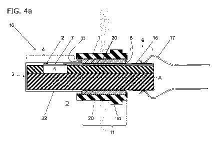
Figures 4a and 4b serve to illustrate the pressure-
tight attachment of the holding ring 1 on the MEMS chip
3. They show respectively a longitudinal section
through a measuring element 10 with a MEMS chip 3 and a
formed cavity 5, and a longitudinal section through a
measuring element 10 with a MEMS chip 3, a formed
cavity 5, and an adjacent channel 21. The measuring
elements 10 are otherwise identical in construction.
As can be discerned in Figure 4a, the MEMS chip 3 is
cast into a holding ring 1 using a casting compound 20,
and is thereby mounted in a mechanically robust manner.
The casting compound 20 completely surrounds and seals
the MEMS chip 3 along the outer periphery in a bushing
region 11. The casting compound 20 permanently connects
the MEMS chip 3 with the holding ring 1 in the bushing
region 11, whereby the holding ring 1 and the casting
compound 20 form a partial encapsulation of the MEMS
chip 3. The bushing region 11, and thereby the casting
compound 20, are arranged between the measuring region
4 and the contact-making region 6 along the
longitudinal axis A. When deployed, the measuring
region 4 is located in a pressure space D that is to be
measured, while the contact-making region 6, when
deployed, is located in an environment at ambient
pressure. The pressure space D is separated by a wall,
represented in Figures 4a - 4b by a grey bar, from the
environment at ambient pressure. The holding ring 1 and
the casting compound 20 thereby form a pressure-tight
CA 02924166 2016-03-11
- 13 -
bushing, whereby instead of disadvantageous attached
bonding wires, here the whole body of the MEMS chip 3
passes through the holding ring 1 and is secured with
the casting compound 20.
Here the holding ring 1 serves to provide simple
manipulation of the measuring element 10, since the
measuring element 10 can be introduced into a pressure
space D simply by contact with the holding ring 1,
without any need to manipulate the measuring region 4.
The measuring element 10 can be attached directly onto
the wall of the pressure space D in a pressure-tight
manner. If a housing 9 is attached onto the holding
ring 1, as shown in Figure 3c, the holding ring 1 can
be indirectly attached onto the wall of the pressure
space D via the housing 9.
In Figures 4a and 4b the holding ring 1 is embodied
with a thickened section 100, which serves as a stop
when attaching the housing 9 onto the holding ring 1,
or when fixing the holding ring 1 directly onto the
wall of the pressure space D. The measuring element 10
can be gripped simply and safely on the holding ring 1
and introduced into a hole in the wall of the pressure
space D, and there secured on the holding ring 1.
Here the holding ring 1 is configured so as to be only
insignificantly longer in the direction of the
longitudinal axis A than the bushing region 11, in
which the casting compound 20 is located. In other
forms of embodiment the holding ring 1 can extend
significantly beyond the bushing region 11 in the
direction of the measuring region 4, that is to say, it
can extend over the whole of the measuring region 4,
whereby the MEMS chip 3 is additionally protected.
The casting compound 20 can take the form of an
CA 02924166 2016-03-11
- 14 -
electrically insulating or conducting mass with as
small a thermal expansion coefficient as possible, in
particular a glass, a ceramic, or an adhesive.
In order to protect the MEMS chip 3 in the measuring
region 4, which is exposed to the medium of the
pressure space D at high temperatures and high
pressures, a passivation layer 32 is arranged here, in
particular an atomic layer deposition passivation layer
32. This ALD passivation layer 32 should be applied to
sensitive surfaces, which, depending upon the
application, can be exposed to an aggressive medium.
Since no delicate bonding wires are arranged on the
contact-making region 6, here a clamping contact 17 can
simply and easily make contact with the contacts 16 on
the atmospheric side of the MEMS chip 3. These clamping
contacts 17 can simply lead to cabling, which is not
represented here.
While the measuring element 10 in accordance with
Figure 4a can be used for the measurement of absolute
pressure, the measuring element 10 in accordance with
Figure 4b, which is of the same design up to the
channel 21, can be used for differential pressure
measurement.
In order to produce an inventive measuring element 10,
a MEMS chip 3, comprising a semiconductor material
composite made from a MEMS substrate 30 and a carrier
substrate 31, is firstly produced. The contacts 16, the
conductors 8, the measuring bridge 19, the
piezoresistive elements 2, together with the membrane
7, are to be arranged in the course of substrate
production, and the semiconductor substrates, 30, 31
are to be fixed to one another. The MEMS chip 3 is then
led through the holding ring 1 in the direction of the
CA 02924166 2016-03-11
- 15 -
longitudinal axis A, and the holding ring 1 is secured
by means of the casting compound 20 over the whole of
the periphery of the MEMS chip 3 in a pressure-tight
manner; here the gap between the surface of the MEMS
chip 3 and the inner surface of the holding ring 1 is
completely filled, whereby the result is a pressure-
tight mounting. Here the casting compound 20 is
arranged in the bushing region 11, between the
measuring region 4 and the contact-making region 6.
In the Figures 1, 3a and 3c here described, any
sharpness of the outer edges of the MEMS chip 3 is
represented as having been removed. Such an optional
configuration of the outer edges of the MEMS chip 3
provides an opportunity for reducing edge stresses, in
particular in the region of the holding ring 1.
It is optionally possible to arrange amplification
electronics on the MEMS chip 3 at a position at a point
on the MEMS chip 3 along the longitudinal direction A.
An arrangement in the vicinity of or in the measuring
region 4 would be best for optimal signal strength, and
freedom from noise and crosstalk, but can only be
achieved with appropriate electronic components that
can be deployed at high temperatures and pressures.
Arrangement of the amplification electronics in the
contact-making region 6, and thus outside the pressure
space D, is the more cost-effective alternative.
Such amplification electronics can be variously
configured and comprise essentially an amplifier,
located as near as possible to the site of the
piezoresistive elements 2, which executes an
amplification of the signals received. In addition to
signal amplification, noise suppression, or further
processing of the measured signals is also possible. An
additional analogue-digital converter enables the
A CA 02924166 2016-03-11
- 16 -
generation of digital signals.
4
. CA 02924166 2016-03-11
1 ,
- 17 -
REFERENCE LIST
S Pressure sensor
Measuring element
1 Holding ring
100 Thickened section
2 Piezoresistive elements
3 MEMS chip
30 MEMS substrate/ SOI substrate
31 Carrier substrate / Si-carrier substrate
32 Passivation layer
4 Measuring region
5 Cavity
50 Bottom wall
6 Contact-making region
7 Membrane
8 Conductor
9 Housing
90 Housing opening
91 External thread
11 Bushing region
12 Further cavity
13 Getter
14 Cabling / sensor cable / outer electrical
conductor
16 Contact
17 Clamping contact
19 Measuring bridge
Casting compound
21 Channel
210 Opening
A Longitudinal axis
D Pressure space