Note : Les descriptions sont présentées dans la langue officielle dans laquelle elles ont été soumises.
CA 02925303 2016-03-23
WO 2015/048486 PCT/US2014/057774
FREQUENCY DEPENDENT LIGHT EMITTING DEVICES
RELATED APPLICATION DATA
The present application claims priority pursuant to 35 U.S.C. 119(e) to
United States
Provisional Patent Application 61/883,710 filed September 27, 2013 which is
incorporated
herein by reference in its entirety.
FIELD
The present invention relates to light emitting devices and, in particular, to
light emitting
devices demonstrating properties related to alternating current voltage
frequencies.
BACKGROUND
Organic thin film electroluminescent (EL) devices, including organic light
emitting
devices (OLEDs), typically operate using constant voltage or direct current
(DC) power sources.
The charge carriers, holes and electrons, are directly injected from high work
function and low
work function metal electrodes, respectively. Several disadvantages exist with
direct current
injection architectures. Direct current injection, for example, can
precipitate charge
accumulation in the recombination zone and large leakage current, resulting in
significant
exciton quenching. Exicton quenching produces low brightness and series
efficiency roll-off.
Further, DC driven architectures require power converters and increase device
sensitivities to
dimensional variations that lead to run away current imperfections. More
importantly, in order
to achieve effective charge injection, high work function metals are required
for anodes, and low
work function metals are required for cathodes. Such requirements severely
restrict suitable
electrode materials for DC devices. Additionally, low work function metals are
unstable in air
and water, thereby increasing fabrication complexities for DC devices.
SUMMARY
Electroluminescent devices are described herein which, in some embodiments,
offer
advantages over prior devices. For example, electroluminescent devices
described herein can be
driven by alternating current (AC), alleviating charge accumulation by the
frequent reversal of
applied bias. Further, electroluminescent devices described herein can provide
radiant
1
CA 02925303 2016-03-23
WO 2015/048486 PCT/US2014/057774
recombination in the absence of direct current injection, thereby breaking
electrode dependency
on high and low work function metals.
Briefly, an electroluminescent device described herein, in one aspect,
comprises a first
electrode and second electrode and a light emitting layer positioned between
the first and second
electrodes. A current injection gate is positioned between the first electrode
and the light
emitting layer or between the second electrode and the light emitting layer.
In some
embodiments, the current injection gate comprises a semiconductor layer of
electronic structure
restricting injected current flow from the first or second electrode through
the semiconductor
layer as a function of alternating current voltage frequency applied to the
first and second
electrodes.
In another aspect, an electroluminescent device described herein comprises a
first
electrode and second electrode and an organic light emitting layer positioned
between the first
and second electrodes. An electron dopant layer is positioned on a first side
of the organic light
emitting layer and a hole dopant layer is positioned on the opposing side of
the organic light
emitting layer, wherein a nanoparticle phase bridges an interface formed by
the electron dopant
layer and organic light emitting layer. Alternatively, the nanoparticle phase
can bridge an
interface formed by the hole dopant layer and organic light emitting layer.
Further, a
nanoparticle phase can bridge an interface formed by the electron dopant layer
and organic light
emitting layer and an interface formed by the hole dopant layer and organic
light emitting layer.
Methods of generating light are also described herein. A method of generating
light
comprises providing an electroluminescent device comprising first and second
electrodes, a light
emitting layer positioned between the first and second electrodes and a
current injection gate
positioned between the first electrode and the light emitting layer or between
the second
electrode and the light emitting layer. An alternating current voltage is
applied to the first and
second electrodes and current injected from the first or the second electrode
is restricted from
flowing into the light emitting layer by the gate as a function of alternating
current voltage
frequency, wherein holes and electrons are radiatively combined in the light
emitting layer.
These and other embodiments are further described in the detailed description
which
follows.
2
CA 02925303 2016-03-23
WO 2015/048486 PCT/US2014/057774
BRIEF DESCRIPTION OF THE DRAWINGS
Figure 1 illustrates a cross-sectional view of an electroluminescent device
according to
one embodiment described herein.
Figure 2 illustrates a cross-sectional view of an electroluminescent device
according to
one embodiment described herein.
Figure 3 illustrates luminance versus AC voltage frequency for
electroluminescent
devices according to some embodiments described herein.
Figure 4 illustrates AC current and luminance versus AC voltage at set voltage
frequencies for electroluminescent devices according to some embodiments
described herein.
DETAILED DESCRIPTION
Embodiments described herein can be understood more readily by reference to
the
following detailed description, examples and drawings. Elements, apparatus,
and methods
described herein, however, are not limited to the specific embodiments
presented in the detailed
description, examples and drawings. It should be recognized that these
embodiments are merely
illustrative of the principles of the present invention. Numerous
modifications and adaptations
will be readily apparent to those of skill in the art without departing from
the spirit and scope of
the invention.
The term "alkyl" as used herein, alone or in combination, refers to a straight
or branched
chain saturated hydrocarbon radical having from 1-20 carbon atoms. In some
embodiments, for
example, alkyl is C8_12 alkyl.
The term "alkenyl" as used herein, alone or in combination, refers to a
straight or
branched chain hydrocarbon radical containing from 2-20 carbon atoms and at
least one carbon-
carbon double bond. In some embodiments, for example, alkenyl comprises C8_12
alkenyl.
The term "aryl" as used herein, alone or in combination, refers to an aromatic
ring system
radical. Aryl is also intended to include partially hydrogenated derivatives
of carbocyclic
systems.
The term "heteroaryl" as used herein, alone or in combination, refers to an
aromatic ring
radical with for instance 5 to 7 member atoms, or to an aromatic ring system
radical with for
instance from 7 to 18 member atoms, containing one or more hetero atoms
selected from
nitrogen, oxygen, or sulfur heteroatoms, wherein N-oxides and sulfur monoxides
and sulfur
3
CA 02925303 2016-03-23
WO 2015/048486 PCT/US2014/057774
dioxides arc permissible heteroaromatic substitutions; such as, e.g., furanyl,
thienyl, thiophenyl,
pyrrolyl, imidazolyl, pyrazolyl, triazolyl, tetrazolyl, thiazolyl, oxazolyl,
isoxazolyl, oxadiazolyl,
thiadiazolyl, isothiazolyl, pyridinyl, pyridazinyl, pyrazinyl, pyrimidinyl,
quinolinyl,
isoquinolinyl, benzofuranyl, benzothiophenyl, indolyl, and indazolyl, and the
like. Heteroaryl is
also intended to include the partially hydrogenated derivatives of the
heterocyclic systems.
I. Electroluminescent Devices
An electroluminescent device described herein, in one aspect, comprises a
first electrode
and second electrode and a light emitting layer positioned between the first
and second
electrodes. A current injection gate is positioned between the first electrode
and the light
emitting layer or between the second electrode and the light emitting layer.
In some
embodiments, the current injection gate comprises a semiconductor layer of
electronic structure
restricting injected current flow from the first or second electrode through
the semiconductor
layer as a function of alternating current voltage frequency applied to the
first and second
electrodes.
In some embodiments, a plurality of light emitting layers are positioned
between the first
and second electrodes. For example, in some embodiments, a plurality of light
emitting layers,
each having a construction selected from Section(s)1B(1)(i)-(iv) and IB(2)
herein, are positioned
between the first and second electrodes. The light emitting layers can have
various emission
profiles that, when combined, provide the desired emission profile
characteristics from the
electroluminescent device. Further, an electron dopant layer can positioned on
a first side of the
light emitting layer and a hole dopant layer can positioned on an opposing
side of the light
emitting layer.
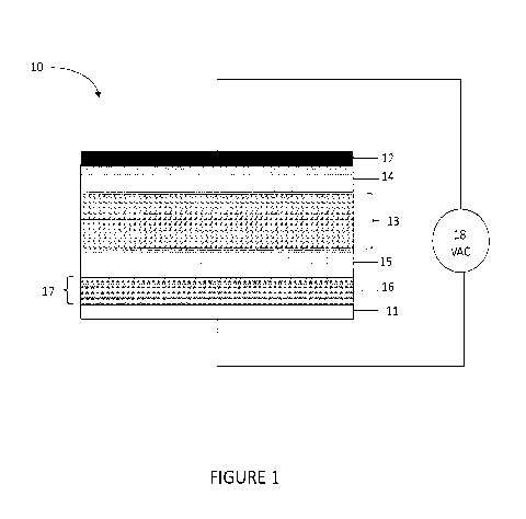
Figure 1 illustrates a cross-sectional view of an electroluminescent device
according to
one embodiment described herein. The electroluminescent device (10)
illustrated in Figure 1
comprises a first electrode (11) and second electrode (12) and a light
emitting layer (13)
positioned between the first (11) and second (12) electrodes. An electron
dopant layer (14) is
positioned on a first side of the light emitting layer (13) and a hole dopant
layer (15) is
positioned on the opposing side of the light emitting layer (13). As discussed
further herein,
electron and/or hole dopant layers, in some embodiments, can be blended
directly into the light
4
CA 02925303 2016-03-23
WO 2015/048486 PCT/US2014/057774
emitting layer, thereby obviating any requirement for discrete layers of
electron donor and/or
hole donor materials. A current injection gate (16) is positioned between the
first electrode (11)
and the light emitting layer (13). The current injection gate (16) can
comprise a layer (17) of
semiconductor material of electronic structure restricting injected current
flow from the first
electrode (11) through the semiconductor layer (17) as a function alternating
current voltage
frequency (18) applied to the first (11) and second (12) electrodes. In
alternative embodiment,
the current injection gate (16) can be positioned between the second electrode
(12) and light
emitting layer (13).
Specific components of electroluminescent devices are now described.
A. First and Second Electrodes
First and second electrodes can be fabricated from any material not
inconsistent with the
objectives of the present invention. As described above, materials for the
first and second
electrodes arc not limited to high and low work function metals required for
prior DC operating
devices. First and second electrodes, for example, can be formed of metal,
such as aluminum,
nickel, copper, gold, silver, platinum, palladium or other transition metals
or alloys thereof.
When constructed of a metal or alloy, the first and/or second electrode can be
reflective or
otherwise non-radiation transmissive. However, in some embodiments, a metal
electrode can be
of thickness permitting the transmission of radiation.
Alternatively, the first and/or second electrode can be constructed of one or
more
materials that are radiation transmissive. Radiation transmissive materials
can pass
electromagnetic radiation provided by light emitting layers described herein
without substantial
interference or attenuation. Suitable radiation transmissive materials can
comprise one or more
radiation transmissive conducting oxides. Radiation transmissive conducting
oxides can include
one or more of indium tin oxide (ITO), gallium indium tin oxide (GITO),
aluminum tin oxide
(ATO) and zinc indium tin oxide (ZITO). In some embodiments, a radiation
transmissive first
and/or second electrode is formed of a radiation transmissive polymeric
material such as
polyanaline (PANT) and its chemical relatives or 3,4-
polyethylenedioxythiophene (PEDOT).
Further, a radiation transmissive first and/or second electrode can be formed
of a carbon
nanotube layer having a thickness operable to at least partially pass visible
electromagnetic
CA 02925303 2016-03-23
WO 2015/048486 PCT/US2014/057774
radiation. An additional radiation transmissive material can comprise a
nanoparticle phase
dispersed in a polymeric phase.
The first electrode and second electrode can demonstrate the same or different
constructions. For example, the first electrode can be non-radiation
transmissive and the second
electrode radiation transmissive. Moreover, in some embodiments, the first and
second
electrodes can both be radiation transmissive or non-radiation transmissive.
In such
embodiments, the first and second electrodes can be fabricated from the same
material or
different materials. Also, first and second electrodes can have any thickness
not inconsistent
with the objectives of the present invention. In some embodiments, first and
second electrodes
have a thickness ranging from 10 nm to 100 gm. Additionally, a layer of
lithium fluoride (LiF)
or lithium oxide (Li20) can be positioned between the light emitting layer and
first and/or second
electrode. For example, a layer of LiF or Li20 can be positioned between an
electron dopant
layer and electrode.
B. Light Emitting Layer
A light emitting layer of an electroluminescent device described herein can
demonstrate a
variety of constructions. For example, a light emitting layer can be an
organic light emitting
layer or inorganic light emitting layer.
(1) Organic Light Emitting Layers
A light emitting layer of an electroluminescent device can be formed of
various light
emitting organic materials as set forth below.
(i) An organic light emitting layer, in some embodiments, comprises a
conjugated
polymeric or oligomeric phase. The light emitting polymeric or oligomeric
phase of an organic
layer comprises one or a plurality of conjugated polymers or oligomers. The
light emitting
polymeric or oligomeric phase, for example, can comprise a blend of conjugated
polymers or
oligomers. In some embodiments, a blend of conjugated polymers or oligomers
comprises a
copolymer of the polymers or oligomers.
6
CA 02925303 2016-03-23
WO 2015/048486 PCT/US2014/057774
A conjugated polymer or oligomer suitable for use in the light emitting
polymeric or
oligomeric phase can comprise at least two repeating units selected from the
group consisting of
repeating units A, B and C:
NV NN R1 R2
________________ (-4110
(A),
R3
R6 R7
=
R4 (B), and
R9
R8
41. O
(C),
wherein represents points of attachment in the polymer chain or oligomer
chain, X is selected
from the group consisting of S, 0, Se and NR5 and RI, R2, R5, R6, R7, R8 and
R9 are
independently selected from the group consisting of hydrogen, C1_20 alkyl,
C2_20 alkenyl, C8_12
7
CA 02925303 2016-03-23
WO 2015/048486 PCT/US2014/057774
alkyl and C8_12 alkenyl and R3 and R4 are independently selected from the
group consisting of
aryl and heteroaryl, wherein the alkyl and alkenyl of RI, R2, R59 R69 R7, R8
and R9 and the aryl
and heteroaryl of It.3 and R4 are optionally independently substituted one or
more times with a
substituent selected from the group consisting of -alkyl, -alkenyl, -aryl, -
heteroaryl, -alkyl-aryl, -
alkyl-heteroaryl, -alkenyl-aryl and -alkenyl-heteroaryl.
In some embodiments, R3 and R4 are independently selected from the group
consisting of
pyridyl, pyranyl, pyridinyl, bipyridinyl, phenylpyridinyl, thienyl, furanyl,
selenophenyl,
fluorenyl, carbazolyl, pyrrolyl, quinolinyl, isoquionolinyl, purinyl, oxazolyl
and isoxazolyl and
oligomers thereof.
In some embodiments, repeating unit A of a conjugated polymer or oligomer
described
herein is selected from the group consisting of:
ZsNN C8H" C8F-117
=
N7sN Cl0H21 C10H21
_a*
\ / ;
NV NN C12H25 C12H25
8
CA 02925303 2016-03-23
WO 2015/048486
PCT/US2014/057774
H3c-H2C-H2c4i2c(H3C-H2c)Hc-H2c
N 7N N CH2-CH(CH2-CH3)CH2-CH2-CH2-CH3
S
41/ MO"
C8H17 C8H17
_________ (
0 C
V NN C10H21 10H21
\
0
NV N C12H25 C12H25
H3C-H2C-H2C-H2C(H3C-H2C)HC-H2C
CH2-CH(CH2-CH3)C12-CH2-CH2-CH3
N7 N N
111
9
CA 02925303 2016-03-23
WO 2015/048486
PCT/US2014/057774
Se
NV \ C8I-117 C8H17
Se
Nr N Cl0H21 Ci8H21
/N
NVSe C,21125
\ C12H25
H3C-H2C-12C-H2C(H3C-H2C)FIC-H2C
Se CH2-CH(CH2-CH3)CH2-CF12-CH2-CH3
IN olio
R5
V
C NN C8H17 8H17
_____________ c 410
CA 02925303 2016-03-23
WO 2015/048486
PCT/US2014/057774
R5
V NN C10H21 C1011121
\
9
R5
NN C12H25 C12H25
; and
H3C-H2C4H2C-N2C(H3C-H2C)HC-N2C
R5-N CH2-CH(CH2-CH3)CH2-CI-12-CH2-CH3
N,
9
wherein R5 is defined hereinabove.
In some embodiments, repeating unit B of a conjugated polymer or oligomer
described
herein is selected from the group consisting of:
11
CA 02925303 2016-03-23
WO 2015/048486
PCT/US2014/057774
N\I
C8H17
I C8H/7
41
C101121
I CioH2i
A440
12
CA 02925303 2016-03-23
WO 2015/048486
PCT/US2014/057774
N
C121.125 C H
-12 25
N
N
CH2-CH(CH2-CH3)CH2-CH2-CH2-0H3
CH2-CH(CH2-CH3)CH2-CH2-CH2-CH3
11 fie
N
;
13
CA 02925303 2016-03-23
WO 2015/048486
PCT/US2014/057774
/ =
C8H17 C8F117
ID"
= /
/ =
CioH21 C101-121
411
= /
14
CA 02925303 2016-03-23
WO 2015/048486
PCT/US2014/057774
/ =
Ci2H26 C12H25
=
= /
/ =
CH2-CH(CH2-CH3)CH2-CH2-CH2-CH3
CH2-CH(CH2-CH3)CH2-CH2-CH2-CH3
slia*
= /
CA 02925303 2016-03-23
WO 2015/048486
PCT/US2014/057774
S
C
C8H17 H17
8
11
S
CioH21
I C101121
___________ 111 *
S
16
CA 02925303 2016-03-23
WO 2015/048486 PCT/US2014/057774
C121125 Cl2H25
= ea.
S
; and
s\
cH2-cH(cH2-cH3)cH2-cH2-cH2-cH3
cH2-cH(cH2-cH3>cH2-cH2-cH2-cH3
***
s
Repeating unit C of a conjugated polymer or oligomer described herein, in some
embodiments, is
selected from the group consisting of:
17
CA 02925303 2016-03-23
WO 2015/048486
PCT/US2014/057774
c8H17 c10H21
c8H17 cloH21
40a. 441a.
Cl2H25 C12H25
and
cH2-cH(cH2-cH3)cH2-cH2-cH2-cH3
H3c-H2c-H2c-H2c(i3C-13C-H2c
.400
Moreover, the selection and molar ratios of repeating units A, B, and C can be
used to
select the emission profile of the conjugated polymer or oligomer, as taught
in Aimsen et al.,
"Synthesis and Electroluminescence Properties of Polyfluorerie Deriatives for
Light-Emitting
Diodes," Proceedings of the 2010 5th IEEE International Conference on
Nano/Micro
Engineered and Molecular Systems, 21-25, the entirety of which is incorporated
by reference
herein. For example, in some embodiments, the repeating units are selected to
provide white
light emission. Alternatively, the repeating units can be selected to provide
green or blue-green
emission.
A conjugated polymer or oligomer of the light emitting polymeric or oligomeric
phase
comprising repeating units A and B can be a conjugated polymer or oligomer of
Formula (1):
18
CA 02925303 2016-03-23
WO 2015/048486 PCT/US2014/057774
R3
R6 R7
/X\
R
R1 2
***
x I
R4
(I)
wherein X, RI, R2, R3, R4, R6 and R7 are defined above and x and y are
integers independently
ranging from 1 to 10,000. As described herein, repeating units A and B of a
conjugated polymer
or oligomer of Formula (I) can be arranged to provide an alternating
copolymer, a block
copolymer, statistical copolymer or a random copolymer. In some embodiments, a
conjugated
polymer or oligomer of Formula (I) has a weight average molecular weight (Mw)
ranging from
about 1,000 to about 1,000,000. A conjugated polymer or oligomer of Formula
(I) can have a
number average molecular weight (Mn) ranging from about 500 to about 500,000.
In some embodiments, a conjugated polymer or oligomer of Formula (I) described
herein
is selected from the group consisting of:
N\I
R6 R7
N/x\ RR 2_
41 = *** Y
9
19
CA 02925303 2016-03-23
WO 2015/048486 PCT/US2014/057774
/
R6
N/ R7
xNN R 1 R2
a 0* ***
x
= /
and
R7
XR6
N/ NN R1 R2
41 1
x
wherein X, RI, R2, R6 and R7 are defined above and x and y are integers
independently ranging
from 1 to 10,000.
In some embodiments, a conjugated polymer or oligomer of Formula (I) described
herein
is selected from the group consisting of:
CA 02925303 2016-03-23
WO 2015/048486 PCT/US2014/057774
c81117
c8H,7
N/SXN C9H17 C81117
4,40 = le**
_ Y
x
11
N\I
C8H17
C81117
-
/0 NN C81117 C8H17
N
olo 11.* ____________________________________________________
_x
c8H17
C81117
¨ Se
/ NN C81.417 C8I1,7
N
0,0 = .1q*
x
9
21
CA 02925303 2016-03-23
WO 2015/048486 PCT/11S2014/057774
p
¨ NI I C8H17 C8E1,7
N/ NN C8H17 C5I-117
. 110" V
_ . 0
____________________________ _ x 1
/
,
/ l'\I
,¨
CicH21 _
I C101121
¨ /SN C101121
N N c 1 0H21
a moo = 10* so
/\ y
_.
_ x ,
,
;
, ,
_ _
cioõ
1 ci,H2,
_ /0N
c,QH2,
N N õAi
I 401,40 = se* c_/)
/\ y
_.
_
,
;
22
CA 02925303 2016-03-23
WO 2015/048486 PCT/US2014/057774
/
---__
_ _
CioH21
1 CioH2i
¨ Se _
/ \
, \a e CioH21
C101121
N N
o, = .** 0
_ Y
_
/ µ 1
U .
9
/
R5 ¨
.0
1 CioH21 C10H21
.¨
¨N/N\N C10121 C10H21
44 e*...
v
,
_
,
,
_
ci2H25 _
1 Ci2H25
¨ /SN
Ci2H25
N N Ci2H25
a 0,40 = it** _______________________________________________________ 0
, \ Y
_
_ x 1
____ ¨
0/
,
23
CA 02925303 2016-03-23
WO 2015/048486 PCT/US2014/057774
Ci2H25
Ci2H25
- /0\Ci2H25
N N C12H25 0
I la*
X
9
N\I
Ci2H25
Ci2H25
¨ Se
N/ "N C12H25 C12H25 0
ii** 4.4*
_
x ,
H3C-H2C-H2C-H2C(H3C-H2C)HC-H2C
CH2-CF(CH2-CF13)CH2-CH2-CH2-CH3
cH2.H(cH2_cm3)CH2.,,2_cH2_cH3
H3c_H2c.H2c_H2c(H3c_H2c)Hc..R2c
N\ 0
=== = *alb_ y
x
24
CA 02925303 2016-03-23
WO 2015/048486 PCT/US2014/057774
H3C-H2C-H2C-H2C(H3C-H2C)HC-H2C
0H2_cH(cH2.cH3)0H2..cF,2_cH2_0H3
p cH2-cH(cH2-cH3)cH2.2-CH2_cH3
H3c_H20_,,2c_H2c(H30_,,2c)Fic_H2c _ _
_
/0\ .
N N
*
/ __ \ a 0*
- x 1
IJ /
,
H3C-H2C-H2C-H2C(H3C-H2C)HC-H2C
CH2-CH(CH2-CI-13)CH2-CH2-CH2-CH3 / N
\
CH2-CH(CH2-CF13)CH2-CH2-CH2-CH3
-........
H3C-H2C-H2C-H2C(H3C-H2C)HC-H2C _
1 _
_
Se
/N N
K)
a 010 Ili liall _________________________________________________
/\ Y
_
_ x 1
\
N / =
'
CA 02925303 2016-03-23
WO 2015/048486 PCT/US2014/057774
H3c-H2c-H2c-H2c(H3c-H2c)Fic-H2c
H3c-H2c-H2c-H2c(H3c-H2c)Hc-H2c cH2.H(cH2_cH3)cH2.H2..cFi2-cH3
cH2_cH(cH2_cH3)cH2_cH2.H2_cH3
N/ \N
1.**= '41**
x
110
C8F117 C81117
/S\ C8I-117
C8I-117
411 P. 1 1.*
x
= /
26
CA 02925303 2016-03-23
WO 2015/048486 PCT/US2014/057774
/ =
C81-111
C8F-117
¨ 0
N/ \NC8H17 C8H17
a leo ____________________________________________________________
x
= /
1110
C8E117
C81117
¨ Se
N/Na C8H17 C81-117 00 = Iwo* ______________________________________ 0
_ Y
x
= /
110
R5
C8F117 G8H17
N
N/ \N C8H/7 C81117
C> IY
x
N.
= /
27
WO 2015/048486 CA 02925303 2016-03-23
PCT/US2014/057774
¨ /sN / 410
/ \ N N Cioi-121
40,40
cioH2, _ N
1 C101421
¨ CloH21 ¨
. it**
4 ________________________________________________________________ (--)
= /
,
\ /
\ =
C101121
N N CioH21 ¨1 _ N
1
C101121 /= N
/0i _
11.4* __________________________________________________________
/
N Y
_
= /
¨ Se / 1110
;
N/ NN Cio1-121
/ \ a 00 ,_ N
C101-121 i Clol-121 C10F121 ¨
. 1.** ( __________________________________________________________ )
N
= /
2.8
.
,
CA 02925303 2016-03-23
WO 2015/048486 PCT/US2014/057774
111110
R,
NC101-421 C/DH21
N/ "N C10H21 C10H21
eio it its*
= /
110
C921125
Cl2H25
/S\ Ci2H25
N N Cl2H25
40,0 = e)**
x
/
9
1110
Cl2H25
Ci2H25
- /0\
N N C12H25 C12H25
= O.
V.
= /
29
CA 02925303 2016-03-23
WO 2015/048486 PCT/US2014/057774
/ 110
----N
-
Ci2H2s
- Se 1 C12H25
Ci2H25
N/ N C121125 \ ____ i
/ \ a 1 Ika* * *** _ Y
_ x 1
N
= /
/ 1110
N
R5 - -
1 1 C121125 Cl2H25
- /NN
Cl2H25
N N C121125 0
< __ \ 1=I k" 1 Pal. . 1 1.4*
_
N
= /
;
/ \ H2-CH(CH2-CH3)CHrCH2-CH2-
CH3
4110
CH2-CH(CH2-CH3)CH2-CH2-CH2-CR3 -----N
H3C-H2C-H2C-H2C(H3C-H2C)HC-H2C CH2-
CH(CH2-CH3)CH2-CH2-CH2-CH3
I
- /S\
N N 0
/ \ 1 itio = slia*
_ , , _ v
___ _
N
= /
,
CA 02925303 2016-03-23
WO 2015/048486 PCT/US2014/057774
/ \ cH2-cH(cH2-cH3)cH2-cH2-cH2-
cH3
110
,...
CH2-CH(CH2-CH3)CH2-CH2-CH2-CH3 N
H3C-H2C-H2C-H2C(H3C-H2C)HC-H2C I
_ CH2-CH(CH2-CH3)CH2-CH2-CH2-
CH3
-
_
0
111 a .. = 1 1 I la* 3
_ x I
N
= /
,
/ \ CH2-CH(CH2-CH3)CH2-CH2-CH2-
C1-13
-....._
CE2-CH(CH2-CH3)CH2-CH2-CH2-CH3 N
H3c-H2C-H2C-H2C(H3C-H2C)HC-112C CH2-CH(CH2-CH3)C1-12-CH2-CH2-C)3
_
r Se
N/ "N 0
0 a **** 1 I la* _ 3
_ x i
N
;
H3C-H2C-H2C-H2C(H3C-H2C)HC-H2C
R5 CH2-CH(CH2-CH3)CH2-0-12-CH2-CH3
/ \ CH2-CH(CH2-CH3)C1-12-C H2-C
H2-C H3
---....
N
CH2-CH(CH2-CH3)CH2-CH2-CH2-C H3
-
II
_
N
N N 0
k" 1 Ia . it" J )'
NI 1
N,...
= /
;
3'
CA 02925303 2016-03-23
WO 2015/048486 PCT/US2014/057774
p
_ 1 _ Cetii7 C8Hi7
- /SN C8H17
N N CO-117
/
a
_
____________________________ L x 1
\ S ;
s\
1 C8H17 C8H17
N/ _
NN C8H17 C8N17
a
/\ Y
_
_ x I
\ S .
9
s\
_ _
1 C81117 C8F117
_
- N/S\N C8H17 C81117
a leo = 0* _________________________________________________________ (_)
/ \ Y
_
\ S .
,
32
CA 02925303 2016-03-23
PCT/US2014/057774
WO 2015/048486
s \
_
_
C8I-117
R5 1 C8I-117
I -
- /NN C8H17
C8H17 (-)
N N
\ / ille* _______________
II le .
/ \ _ Y
- x 1
\ S .
,
s\
-
_
Ci0H21
I Ciolizi
- S
N/ NM C10H21 C10H21 ___________________________ ( ___ )
/\ I 14/ 1 la. 4 1 I la* - y
_ x 1
\ S .
9
S \
...0101-121
1 010E421
--
- 0
/ N C10H21 C10H21 c igi ________________
N N
0 ________________________________________________________________ K )
\ / ____________ <! _
x
_ 1
\ S ,
33
CA 02925303 2016-03-23
WO 2015/048486 PCT/US2014/057774
s\
1 C101121 C101121
¨Se
N/ "N CioH21 Ci0H21
a ono = leo ________________________________________________________ 0
, \ _ Y
_ x 1
\ S .
,
p
R5 ¨
I 1 C1 0H21
c,0H2, ¨
¨ N
N/ \N Ci0H21 Ci0E21
,\a
= __________________________________________________________________ OP* 0
Y
-
_ x 1
\ S .
9
p
.- 1 ¨ Ci2H25 Ci2H25
¨ N/S \N C12F25 C12R25
, \a0*
_
= __________________________________________________________________ it** 0
Y
_
_ x 1
____ _
C( .
,
34
,
CA 02925303 2016-03-23
WO 2015/048486 PCT/US2014/057774
s \
_ _
1 Ci2H25 012N25
- /0\
N N C121125 C12H25 (-)
/ \a el*
31
_
- x 1
\ S .
/
s\
_ -
1 C121125 C121425
- Se
N/ NN C12H25 C121-125 1 N ______ ( __ )
/ \a le Y
_* = Mk
x 1
\ S .
/
s\
R5 - -
- NI I Cl2H25 Ci2H25
N/ NN C12H25 Ci2H25
I io* sp. 40* ______________________________________________________ 0
/ \ Y
_
x 1
\ S .
/
CA 02925303 2016-03-23
WO 2015/048486 PCT/US2014/057774
H3C-H2C-H2C-H2C(H3C-H2C)HC-H2C
s\
cH2-cH(cH2-cf13)cH2-cH2-cH2-cH3
cH2-cH(cH2-cH3)ci-f2-cH2-cH2-cH3
H3c-H2c-H2c-H2c(H3c-H2c)Hc-H2c
N/sNN
________ a 14 1* 1 141.
x I
S
H3C-H2C-H2C-H2C(H30-H2C)HC-H2C
cH2-cH(cH2.cH3)cH2-C.2.cH2.cH3
.2.H(cH2_cH,õ2_cH2_cH2.,,,
H3c_H2c_H2c_H2c(H3c_H2c),A.H2c
0
N/N ita*
a IP y
x
S
H3C-H2C-H2C-H2C(H3C-H2C)HC-H2C
C
CH2-CH(CH2-CH3)CH2-CH2-CH2-CH3 H2-CH(CH2-
CH3)CH2-CH2-CH2-CH3
H3C-H2C-H2C-H2C(H3C-H2C)HC-H2C
Se
4 TO".
S
and
36
CA 02925303 2016-03-23
WO 2015/048486
PCT/1JS2014/057774
H3c-H2c-H2c-H2c(H3c-H2c)Hc-H2c
H3c-H2c-H2c-H2c(H3C-13C-H2c
CH2-CH(CH2-CF13)CH2-CH2-CH2-CH3 cH2
cH(cH2-cH3)cH2-cH2-cH2 cH3
R5
N/ \N
al 4.4*
V
x
wherein R5 is defined hereinabove and x and y are integers independently
ranging from 1 to
10,000.
A conjugated polymer or oligomer of the light emitting polymeric or oligomeric
phase
comprising repeating units A and C can be a conjugated polymer or oligomer of
Formula (II):
R
R8 9
R1 R2
NVxNN
_ x
(II)
wherein X, R1, R2, Rg and R9 are defined above and x and y are integers
independently ranging
from Ito 10,000. As described herein, repeating units A and C of a conjugated
polymer or
oligomer of Formula (II) can be arranged to provide an alternating copolymer,
a block
copolymer, statistical copolymer or a random copolymer.
In some embodiments, a conjugated polymer or oligomer of Formula (II) has a
weight
average molecular weight (Mõ,) ranging from about 1,000 to about 1,000,000. A
conjugated
polymer or oligomer of Formula (II) can have a number average molecular weight
(MO ranging
from about 500 to about 500,000.
In some embodiments, a conjugated polymer or oligomer of Formula (II)
described
herein is selected from the group consisting of:
37
CA 02925303 2016-03-23
WO 2015/048486 PCT/US2014/057774
c8h,7
_ -1 c81117
/s\ 8F117
c8H,7 ,
N N c
0 _________ a le* _ x -
_ Y
_
;
_ _ C8H97
C8F197
/0\ C81117
C5H17
N N - a*
\ / 0
/\111 \/1110 _____________________________
_ x - \ ______________________________________ /
-y
- ,
_ _ C5H17
Ce1197
Se
N/ NN C8H17 C81117 (-)
/\ It" el* _ X - C1,1* __________________________________
_ Y
=
9
_ -
R5
-
I _
C5H17
C5H17
_
N
N/ \N Celli7 C81497
____Ip*
\ / N ________________________________ \ /
11 ________ = ______ c_fillt
_ _
/'
x \ /
_ Y
_ ;
_
_ C101121
_
C10H21
/S\CloH21 C10N21
.a 40* _ x _ \ /
Y
_ ;
38
CA 02925303 2016-03-23
WO 2015/048486 PCT/US2014/057774
¨ _ Ci0H21
CioH21
0
N/ \N C10H21 C10H21
\ / 0
\ = *** ________________________________________________ (-1/11111*
Y.
_ x - _
,
_ C101121
-
CioH21
Se
N/ \N C101121 Ciolizi
\ i 0
/\ ilk 404 _____________________________________________ (-II*
_ y
_ x - .
,
_ -
R5
-
CiaR21
1 - CI0H21
N
N/ \N C10H21 C101121
\ i 0
/\ /110 IP* ____________________________________________ di*
_ Y
_ x -
- _
- - C12H25
Ci2R25
S
N/ \N C12H25 C1211250
11 ____________ ilk" ___________________________________ *** _ X - (-1/11"111
- '
_
,
39
CA 02 925303 2 016 -03-2 3
WO 2015/048486
PCT/US2014/057774
_
_ ci2H25
Ci2H25
N/ 0\
N Ci2H25
Ci2H25
/\i it** _ X _ (11411* _
y 0
- ;
_ -
- - C121125
Ci2H25
Se
N/ \ N C 1 2H25 C121125
0
0 __________ 4 If**
_
_ X
_
,
¨ _
R5
-
I _
Ci2H25 C121125
N
N/ \N C12H25 C121125
\ / 0
/\ ilk ealk __________________________________________ dr"
-
_ X -
13C-H2C-H2C-H2C(H3C-H2C)HC-H2C CH2-CH (C
H2-C H3)CH2-C H2-C H2-C H3
C 2-CH (CH2-CH3)CH2-C H2-CH2-CH3
H3C-H2C-H2C-H2C(H3C-H2C)HC-H2C - -
- -
/S\
N N
\ / 0
/ __ \ ilk /I** _________________________ cll.
_ Y
-
_ x .
/
CA 02925303 2016-03-23
WO 2015/048486 PCT/US2014/057774
H3c-H2c-H2c-H2c(H3c-H2c)Hc-H2c CF12-
CH(CH2-0-13)CH2-CRTCH2-CH3
CR2-CH(CHTCH3)C112-CF12-CR2-CH3
H3C-H20-R2C-H2C(R3C-R2C)R0-R2C
N/ \N
a ____________________ lila* _ x " _
H3C-H2C-H2C-H2C(H3C-H2C)HC-H2C CH2-
CH(CH2-CH3)CH2-CH2-CH2-CH3
CR2-CH(CH2-CR3)CR2-CR2-CH2-CH3
H3C-H2C-H2C-H2C(H3C-H2C)K-R2C
Se
N/
0
and
HC-H2c-H2c-H2c(H3c.-H2c)Fic-H2c CH2-CH(CH2-CH3)CH2-CH2-CH2-CH3
H3C-H2C-H2C-H2C(H3C-H2C)HC-H2C
CH3
CH2-CH(CI-12-CH3)CH2-CH2-CH2
R5
N
\
44/ *olio ___________________________________
x
wherein R5 is defined hereinabove and x and y are integers independently
ranging from 1 to
10,000.
A conjugated polymer or oligomer of the light emitting polymeric or oligomeric
phase
comprising repeating units B and C can be a conjugated polymer or oligomer of
Formula (III):
41
CA 02925303 2016-03-23
WO 2015/048486 PCT/US2014/057774
R3 Rg
1/ R8
Re R7
410 _______________________________________________________________
_ x _ Y
R4
(III)
wherein R3, R4, R6, R7, Rg and R9 are defined above and x and y are integers
independently
ranging from Ito 10,000. As described herein, repeating units B and C of a
conjugated polymer
or oligomer of Formula (III) can be arranged to provide an alternating
copolymer, a block
copolymer, statistical copolymer or a random copolymer.
A conjugated polymer or oligomer of Formula (III) can have a weight average
molecular
weight (1V1,) ranging from about 1,000 to about 1,000,000. In some
embodiments, a conjugated
polymer or oligomer of Formula (III) has a number average molecular weight (KJ
ranging from
about 500 to about 500,000.
A conjugated polymer or oligomer of Formula (III) described herein can be
selected from
the group consisting of:
42
CA 02925303 2016-03-23
WO 2015/048486
PCT/1JS2014/057774
RB R9
R7
R6
(-1/111110 ___________________________________________________
- Y
_ x
t(j
4104
R9
R9
R6 R7
(-MO
___________________ ONO
- Y
_ x
/
and
43
CA 02925303 2016-03-23
WO 2015/048486 PCT/US2014/057774
p
R9
R9
- -
1 0 ____________________________________ c R6 R7 ____________ 4110 (--)
coo
_ _ Y
_ x
1
C(
wherein R6, R7, Rg and 1Z9 are defined above and x and y are integers
independently ranging from
1 to 10,000.
In some embodiments, a conjugated polymer or oligomer of Formula (III)
described
herein is selected from the group consisting of:
p
_
c8H,7 _
_ _
c8H17
I c8Hi, caHl7
clill* _______________________________________________________ 0
,
_
1 -
(I ;
44
CA 02925303 2016-03-23
WO 2015/048486
PCT/US2014/057774
pi
_
_
cioH2,
ci0H21 _
_
1 c10'-'21 c10H21
opio __________________________________________________________
( __ \ it iii.10 _ 0
_ y
x
_
I _
0/
,
-
p
_ _
Ci2H25 _
Ci2H25
ICi2H25 C121-125
( __ \ . lia* - -y
x
_
1 _
r(i .
9
1-13C+12C-H2C-H2C(H3C-H2C)FIC-H2C
CH2-CH(CH2-CH3)CF12-CH2-CH2-CH3
p
_ H,c_H2c_H2c_H2c(H3c_H2c)Hc_H2c
cH2_.(cH2_cH3)cH2_cH2cH2_cH3
_
1
I di" _____________________ 1
( __ \ . lia* _ _ Y
x
_
1 _
I(J .
1
CA 02925303 2016-03-23
WO 2015/048486 PCT/US2014/057774
/ 10
C8F117 _
¨ ----N ¨ _
C8F117
C8H17
I C8H17 (¨I).* __________________ 0
( __ \ . *** _ Y
x
_
I _
N--...
= /
9
/\
¨ N ¨ _
CioH21 _
CioH21
C10F121
0
I
C1
OF121
( ________________________________________ \ . le* - -y
x
_
1 ¨
N--._.
= /
9
/ =
¨ ----N ¨ _
C121-125
_
Ci2H25
Ci2H25
I Cl2H25 clip* ____________ ( ____ )
( ________________________________________ \ li *** _ -y
x
_
1 ¨
N¨...._
= /
9
46
CA 02925303 2016-03-23
WO 2015/048486 PCT/US2014/057774
13C-H2C-H2C-H2C(H3C-1-12C)HC-H2C
CH2-CH(C12-CH3)CH2-CH2-
CH2-CH(C12-CH3)CH2- CH2-CH3
/ =
CH2-CH2-CH3
CH2-CH(CH2-CH3)CH2-
CH2-CH2-CH3
- ---"Ni - _
I Op* ____________________ 0
*** _ _
,
_
I _
N
= /
,
p
coil7 _
_ _ _
c8H,7
1 co-117 c8H17
op* _________________________________________________________ 0
( _______________________________________ \ . *** _ -y
x
_
1 -
C(
,
p
_ _ _
c10H21 c10H21
1 C10H21 C10H21
Op* _________________________________________________________ 0
( _______________________________________ \ . ..* _ r
_
1 _
cf
;
47
CA 02925303 2016-03-23
WO 2015/048486
PCT/US2014/057774
p - C12H25 _
- -
Ci2H25
I -)
Cl2H25 Cl2H25
__________________________________________ Cal* __________________
_ (
x
-
1 -
S
'
and
H3c-H2c-H2c-H2c(H3c-H2c)uc-H2c cH2-cH(cH2-cH3)cH2-cH2-cH2-cH3
p H3c-H2c-H2c-H2c(H3c-H2c)Hc-u2c cH2-
cu(cH2-cH3)cH2-cH2-cti2-cH3
- -
_ _
(¨) ________ li lia* ___________________ _cal*
-y
x
_
1 _
- S
wherein x and y are integers independently ranging from 1 to 10,000.
A conjugated polymer or oligomer of a light emitting polymeric or oligomcric
phase
comprising repeating units A, B and C can be a conjugated polymer or oligomer
of Formula
(IV):
/R3 --
R9
Rs
1 -
- R2 - R6 R7 - _41110 _________
, X ,
N N Ri
a* ii _________________________________________ \ __ / . ititio le le _ z
_
_ -, -,1 _ Y
Ri
48
CA 02925303 2016-03-23
WO 2015/048486 PCT/US2014/057774
(IV)
wherein X, RI, R7, R3, R4, R6, R7, Rg and R, are defined above and x, y and z
are integers
independently ranging from 1 to 10,000. As described herein, repeating units
A, B and C of a
conjugated polymer or oligomer of Formula (IV) can be arranged to provide an
alternating
copolymer, a block copolymer, statistical copolymer or a random copolymer.
In some embodiments, a conjugated polymer or oligomer of Formula (IV) has a
weight
average molecular weight (Mw) ranging from about 1,000 to about 1,000,000. A
conjugated
polymer or oligomer of Formula (IV) can have a number average molecular weight
(MO ranging
from about 500 to about 500,000.
In some embodiments, a conjugated polymer or oligomer of Formula (IV)
described
herein is selected from the group consisting of:
R9
_ - R6 R7 R8
41110
,X, R2
N N Ri
1 /
# .1111. = 400 __ _ z
- _ Y
N
/ 10,
R9
R6 R7 R8
R2 411*
N N
1 /
OS \_,1111110
\ _ Y
= /
and
49
CA 02925303 2016-03-23
WO 2015/048486
PCT/US2014/057774
p
1 R6
-
- R9 _
R9
R7
-
õX R2
N 'N Ri
__________________________________________________ 1010 ________ =
\-S
wherein X, RI, R2, R6, R7, R8 and R9 are defined above and x, y and z are
integers independently
ranging from Ito 10,000.
For example, a conjugated polymer or oligomer of Formula (IV) described herein
can be
selected from the group consisting of:
p _ r.9. C8H17 -
,,,4i7
,
_ - - I C8H17 C9F117 =10
''NN C8I-117
C9H17
11140 *
1.
. iiii, .O. # II _
_x _ 1 _ y
d ;
pi __. ci0H21
uioH21
-
C
I c10H21 10 21 _
H
-
0
,S,
N N Clol-121 Ci0F121 -
.
41110 ________________________________________ (¨MO
\ / 7
IF ./pOl .."...
Ilit
d ;
CA 02925303 2016-03-23
WO 2015/048486
PCT/US2014/057774
p _
C -
C12H25 i2H25
-- - - I Cl2H26 C12H25
S Ci2H25
N' NN C121-125 * ¨01110
*
aOt ________________________________________________________ .
= ii 0. \/ _ _ z
-',i.-
U =
,
H3C-H2C-H2C-H2C(H3C-H2C)HC-H2C CH2-CH(CH2-CH3)CH2-CH2-CH2-CH3
CH2-CH(CH2-CH3)CH2-
CH2-CH2-CH3
N _ cHrcH,H,
cH2_,H2_cH3)cH2-
_
H3c.2.H2c_H2c(H3c_H2c)H,H2c
/
H3C-H2c_H2c_H2c(H3c_H2c).2c
I
.
_
N. _ _A.N ONO
a*
.
* *
_ _ z
ii O.
_x _ I _}
d
, ,,,,
_
c8F,17
caH,7
c,H17
_ _ I õHi., _
,o, c8H17 1 N
N N C8H)7
# .OI
_ z
0 e moo
_
/
0
N / =
9
51
CA 02925303 2016-03-23
WO 2015/048486
PCT/US2014/057774
p_
co2, c10H21 _
_ I cioH c
zi 10H21 _als
,0,, C101-121 _
0
_
N- N C101121
_ z
= 11" It"
0/
N /
;
p _
Ci2H25
Ci2H25 -
i--\-
Ci2H25
- - - I 012H25
0, C
N' N C 12H25 l2H25
*
_________________________________________________ a. _________ i
-z
N/ =
9
H3C-H2C-H2C-H2C(H3C-H2C)HC-H2C CH2-CH(CH2-CH3)CH2-CH2-CH2-CH3
CH2-CH(CH2-CH3)CH2-
CH2-CH2-CH3
N
cH2_GH(cH2_cH3).H2_
chircHrcH,
_
H3c_H2c_H2c_H2c(H3c_H2c)Hc_H2c ,
H3c_H2c-,_,2c_H2c(H,c_H2c),,c_H2c
I , __ ,_
_ _ olio 1 vii
õo,
. Nii so..
* _44
\ ____________________________________ , _ z
-y
/
0
N /
52
CA 02925303 2016-03-23
WO 2015/048486
PCT/US2014/057774
p _ C8n ., coi7 -
17
- - - I C81-1/7 C8H17
- 01110 __ .
,Se
C8H17
N iki C,-i7 olio . 00
_.
_x _ ,
(-.
"
=
,
p _
u ci,H2, -
C15,121
- - I C/0H21 C/OH21 -, ie. ___________ 0
Se
N-, =N CioH21 C10H21
11111*
olio it = _z
,...õ,
"
=
,
N
_
u Ci2H25
C1 r,25
- 411. _________________________________________________________ =
- - - I C/2H25 C12H25
,Se C12H25
N 'N C12H25
\ _______________________________________________ /
\ /
is ii -** * \--/a. - _ z
_x _ , _,
,-;N e
=
,
53
CA 02925303 2016-03-23
WO 2015/048486 PCT/US2014/057774
H3C-H2C-H2C-H2C(H3C-H2C)HC-H2C CH2-CH(CH2-C1-13)CH2-CH2-CH2-CH3
CH2-CH(CH2-CH3)CH2-
CH2-CH2-CH3
/c3 - CH2-CH(CH2-
CH3)CH2-
_
CH2-CH2-CH3
H3C-H2C-H2C-H2C(H3C-H2C)HC-H2C
H3C-H2C-H2C-H2C(H3C-H2C)HC-H2C
I /¨ __ \
- _ -
N N
,Se. O=10 __ µ i
w
. 4 amio
* ,
-N,:- I _ _
3.
u
p _
C5F117
R5 C5H17
- I - I C81-117 C8F117
-
N", IV C81-117 C8H17
. e 10õ. = 0* _ \/as ____________________________________________ z0
_ x =_ 1 _
d .
9
P _ .., . . C101121
R5 t,10r121
- I - - I C101121 C10H21
- _______________________________________________________________ - alill 0
N
N",, -N CioF121 C10H21 O. _\/
0 11" 10. " _______________________________________________ z
¨ix - 1 _ Y
L)
;
54
CA 02925303 2016-03-23
WO 2015/048486
PCT/US2014/057774
p ci2H25
R5Ci2H25
I 1 Ci2H25 C12H23
-
N -110 O-
N' %N Ci2F125 C121125 _ ______________________
z
-x _ 1 _
d .
9
H3C-H2C-H2C-H2C(H3C-H2C)HC-H2C CH2-CH(CH2-CH3)CH2-CH2-CH2-CH3
CH2-CH(CF12-CH3)C142-
CH2-CH2-CH3
N
cHrcH(cH2.H3).,2_
cHrcH2_cH,
H3c_H2c_H2c+,2c(H,c_H2c)Ficti2c , _
H3c_H2c.H2c_H2c(H3C_H2c)c_H2c
I _
_ _ _ _a0
,,NR5 \ 0
. NI,ii leo
* * ________________________________________________
a0
- ________________________________________________ \ /
_ z
-'i-
U
/ 110
"Ths1 C8H17 _
C81117 /--\
1 C8F117 C8I-117
_
S _ _
C8F117
=
N,, N C8H17
ii. 4õ,* = IP* ,
õ \ _ Y
N
= /
;
CA 02925303 2016-03-23
WO 2015/048486 PCT/US2014/057774
--N
* /..111:CiO0F121 C10H21 -
CioH21
ICion21 _
,S, Cio1121 4011.1 0
N N CioH2i
is 4 itito _,
_
N
= /
,
/ AP
---N - C12H25 -
Ci2H25
Ci2H25
- - I Cl2H25 -
.,S, C12H25 -*ill ___________ 0
N N Cl2H25
* 100 \ __________________________________________ /
µ /_411110
_ Z
\) -
-.--- /i--- /
X [ \ _Y
N
= /
;
N3C-H2C-H2C-H2C(H3C-H2C)FIC-N2C CH2-CH(C12-CH3)CH2-CH2-C1-12-CH3
CH2-C(CH2-CH3)CH2-
N3C-H2C-H2C-H2C(N3C-H2C)HC-H2C ii H
CH2-CH2-CH3
'''' N CH2-CH(CH2-
i
H3C-H2C-H2C-H2C(H3C-H2C)HC-H2C \ _ CH3)C1-12.-
.CH2-CH2-
CH3
I
- _
S, IOO __________ 0
N' N * ¨ " \ ______________ /
. * ¨.110
\ __________________ / / _ -z
x \ -y
N
= /
56
CA 02925303 2016-03-23
WO 2015/048486 PCT/US2014/057774
/ =
-Thl _
C8H17 -
C8H17 r--\-
1 Cgr-ii7
õ j C8H17 =10 ____ \ ___ i
-
NA N C8F117 C8H17
all* *
. .4. 0,40 = = _=_ L
N
= /
9
/ =
ClOH21
IN
C10H21 C101121 / __
- I C10r121 -
at* _____________________________________________________________ u
N N Cio1121 C10H21
er. W
. 4 40,40 = = _ _ z
, \ _ Y
N
= /
;
/ =
--N _
C12H25 C12H25 -
1 C12H25 C12H25
-
-
A.
N" N C12H25 C121125
. a es . 0* _________________________________ _ 0
oalo
_ z
, \
N
= /
;
57
CA 02925303 2016-03-23
WO 2015/048486
PCT/US2014/057774
cH2-CH(cH2-CHDCH2-CH2-CH2-CH3
H3c-H2c-H2C-12C-H2c)HC-H2c
cH2-cH(CH2-CH3)CH2-
H3c-H2C-H2c-H2C(H3C-H2C)Hc-H2c 110
CH2-cH2-cH3
H3c-H2c-H2C-H2c(H3c-H2c)Hc-H2c --- N
\ I CH2-CH(CH2-
CH3)CH2CH2-CH2-
CH3 :
I
___________________________________________________________________ 4.4140 0
_
_
-0,
. ¨**
/ _ z
x \ -y
N
/
/ 110
--N _
C8H17 -
C8H17
_ I C8H17 C8H17
_ _411140 _________________________________________________
,Se C8H17 =
N =N CsHi7
4111. \/
k /
ilk ilk Olt* 11 II/ -z
X \ -y
N
= /
/
/ =
--N _
Ciolti -
CioH21
I C1
0
H21 C10H21 _ 014 __________________________________________ 0
,Se CioH21
N IV cioH2, _is
ii 4 es \/ \ ____________________ , _ _ z
x \-y
N
= /
,
58
CA 02925303 2016-03-23
WO 2015/048486
PCT/US2014/057774
/ \110
---N - ,., , , C121-125 -
L121725
_
I ci2 C H
H25 12 25
¨111 _____________________________________________________ 0
_ _______________________________________________
,Se Ci2H25
N =N C121-125\10
/
411 ii. le* it \__;11110#
_ -z
N....õ
= /
,
1-13C-H2C-H2C-H2C(H3C-H2C)HC-H2C CH2-CH(CH2-CH3)CH2-CH2-CH2-CH3
CH2-CH(CH2-CH3)CH2-
H3C-H2C-H2C-H2C(H3C-H2C)HC-H2C .
CH2-CH2-CI3
="' ' N CH2-CH(CH2-
H3C-H2C-H2C-H2C(H3C-H2 1 C)HC-H2C N. -
CH3)CH2=CH2-CH2-
CH3
I
_
Se __________________________________________________________
. i_ =N Itaio . *** _ - \.=
/
_ z
x \ -y
N
= /
/ =
-'-14 C8H17 -
R5 C8H17
- 1 I C81-117 C8H17 -
\,l
¨al N .
N CeHi7
# .11110.----*
ICõ NN CsHi7
. ii a÷
_
.õ \ _ ),
N
= /
;
59
CA 02925303 2016-03-23
WO 2015/048486
PCT/US2014/057774
/ =
--N L, CloH21 -
R5 Ci0n21 f---\--
- I I C1
0
H2 1 C1
0
H21 _
_N.. C10H21
MOO __________________________________________________________ i
N 'N C10H21
= ii *** * ." _
_z
x \ -y
N
= /
=
9
=
-"N _
Ci2H25 -
R5 Ci2H25
- I I Ci2H25 Cl2H26
-
,N C12H25 ¨0110 ___________ 0
N" 'ts/Ci2H25
* MO* \/
= ii leo
_z
_
x \ _y
N
= /
,
H3C-H2C-H2C-H2C(H3C-H2C)HC-H2C CH2-CH(CH2-CH3)CH2-CH2-CH2-CH3
H3C-H2C-H2C-H2C(H3C-H2C)HC-H2C
* \ CH2-CH(CH2-
CH3)CH2-
CH2-CH2-CH3
==-- N CH2-CH(CH2-
I
H3C-H2C-H2C-H2C(H3C-H2C)HC-H2C N _ CH3)CH2=CH2-
CH2-
CH3
_a* .
_
,N¨R5 I
x \ -y
N.,...
= /
CA 02925303 2016-03-23
WO 2015/048486
PCT/US2014/057774
S
CeHõ C8I-117
=
CeHõ C8H17
ipa*
CeHõ N CeHõ
ipito
x
S
ciaH2i CioH21
N
I C10H21 C101-121
110140
CioH21 N CioH21
/
= = O.
x
5
C12H25
C12H25
I Cl 2 H25 C 2 H25
,
C 2H25
414 111
N Cl2H25
4111 lipa*
X I
S
5
61
CA 02925303 2016-03-23
WO 2015/048486
PCT/US2014/057774
H3c-H2c-H2c-H2c(H3c-H2c)Hc-H2c cH2-cH(cH2-cH3)cH2-cH2-cH2-cH3
CH2-CH(C1-12-CH3)CH2-
CH2-CH2-CH3
0 CH2-CH(CH2-CH3)CH2-
_
H3C-H2C-H2C-H2C(H3C-H2C)HC-H2C _ CH2-CH2-CH3
H3C-H2C-H2C-H2C(H3C-H2C)HC-H2C
I
- _
N N
= ii or* = le _ _ z
\ S
P
- C8H17 -
C8H17
- _ - 1 C8I-117 C8H17
koio _____________________________________________________________ ,
0, C8H17
N. N C8H17
-z
_ Y
OS
;
P
- Ci0H21
CioH21
H
Cio21 _at. ____________ .
- - I Ci0H21
A. CioH21 _
N N Cio1121 ¨0110 - \ __ /
z
-x _ 1 -y
CCS .
,
62
CA 02925303 2016-03-23
WO 2015/048486
PCT/US2014/057774
s\
_
C12H25 C12H25 -
C 25
- 1 Cl2H25 - _
12Has
,O, Ci2H25
. \,õ
N A C121-125 \ __ /
is 4 [ ,
)õ
_ _z
_ Y
CCS .
,
H2-CH(CH2-CH3)CH2-CH2-CH2-CH3
CH2-CH(CH2-CH3)CF12-
H3C-H2C-H2C-H2C(H3C-H2C)HC-H2C CH2-CH2-CH3
H3C-H2C-H2C-H2C(H3C-H2C)HC-H2C
)..._ CH2-CH(CH2-
CH3)CH2-CH2-CH2-
CH3 _
H3C-H2C-H2C-H2C(H3C-H2C)HC-H2C
I
-o
__________________________________________________
\
/-4100 __ 0
. Ni c 1 to 0 . =¨a ________________________________
\ / µ /
-z
_ x _ 1 -y
C(
p _
C
C8H17 8H17
_ _ I C8H17 C81.117
_
,SeC8H17N e 'N C81-117
4111.1 ______________ _ *** ( )
. .=40 I), le z
x _ , _Y
OS
=
,
63
CA 02925303 2016-03-23
WO 2015/048486 PCT/US2014/057774
jp
_
cloH21
cloH21 -
- - CloH21
1 CioH21 -I .44
,Se C /0H21
N =N C 1 oF121 _ Ail"
ill*
X /
ili, /I .1111410 . 4. z
_ x _ 1 _ y _ _
CCS
;
p
-
Ci2H25
Ci2H25 -
_ - - . al / I CI C12H25
2H25
,Se Cl2H25
N . N C12H25 _________ ai ____ \ / ii *as = it _ _ z
_.,
Os
;
H3c_H2.2.H2c(_,3c_H2c),,c_H2c cH2_cH(cH2.H3)cH2_cH2_.H2.cH3
CH2-CH(CH2-CF13)CF12-
CH2-CH2-CH3
S)D CH2-CH(CH2-
CH3)CH2-
/ CH2-CH2-CH3 -
H3C-H2C-H2C-H2C(H3C-H2C)HC-H2C -
H3C-H2C-H2C-H2C(H3C-H2C)HC-H2C
( ¨4111.
\/)
_ -
,Se
=
N - - N
4 _ _ \ __ / _z
, = =4=IS
CC
64
CA 02925303 2016-03-23
WO 2015/048486 PCT/US2014/057774
P
C81117
R5 C8[117
I - 1 C51-117 C8H17 -
N C8H17 _ 41 _____
N., , N C8F117 \ __ /
110 0
. ii 400 le le
=No
_ z
os
;
p
_
cioHzi -
R5Ci0H21
- I - - 1 C101-121 C10H21
-
N CioHzi
N",, -N CioHzi
_x _ # /el ilik
a.
_ z
46 ii 00 _
, _Y
OS .
9
p C121125
R5 Ci2H26
- I - - 1 Cl2H25 Ci2F125
- ________________________________________________ =140 N, Ci2H25
N", N Ci2H25 It AlliS
II
00 \ ______________________________ , _ z
_ Y
CCS .
,
and
CA 02925303 2016-03-23
WO 2015/048486 PCT/US2014/057774
HC-H2c-H2c-H2c(H3c-H2c)Hc-H2c cH2-cH(cH2-cH3)cH2-cH2-a-42-cH3
0-12-cH(cH2-c1-13)0-12-
cH2-cH2-cH3
s).D CI-12-
cH3)cH2-
cH2-cH2-CH3
H3c-H2c-H2c-H2c(H3c-H2c)Hc-H2c
H3c-H2c-H2c-H2c(H3c-H2c)Hc-H2c
ONO _______________________________________________________________
- -
N
_
I _ Y
wherein R5 is defined hereinabove and x, y and z are integers independently
ranging from 1 to
10,000.
Conjugated polymer or oligomer of the light emitting polymeric or oligomeric
phase
comprising at least two repeating units selected from the group consisting of
repeating units A,
B, and C described herein can be synthesized using methods known in the art.
For example, in
some embodiments, a such conjugated polymer or oligomer can be provided using
Suzuki
coupling. Additional information regarding conjugated polymers and/or
oligomers comprising at
least two repeating units selected from the group consisting of repeating
units A, B and C
described herein is provided in Patent Cooperation Treaty Application
Publication
W02012/009344 (PCT Application No. PCT/US2011/043690, filed on July 12, 2011),
which is
hereby incorporated by reference in its entirety.
Moreover, conjugated polymer or oligomer of the light emitting polymeric or
oligomeric
phase can comprise one or more species of polyfluorenes, polyflouorene
copolymers and/or
derivatives thereof. In some embodiments, a conjugated polymer or oligomer of
the polymeric
or oligomeric phase is selected from the group consisting of poly(9,9-di-n-
octylfluoreny1-2,7-
diyl), poly[(9,9-di-n-octylfluoreny1-2,7-diy1)-alt-(benzo[2,1,3]thiadiazol-4,8-
diy1)], poly(9,9-di-
n-dodecylfluoreny1-2,7-diy1), poly(9,9-di-n-hexylfluoreny1-2,7-diy1), poly(9,9-
di-n-
octylfluoreny1-2,7-diy1), poly(9,9-n-dihexy1-2,7-fluorene-alt-9-phenyl-3,6-
carbazole), poly[(9,9-
dihexylfluoren-2,7-diy1)-alt-(2,5-dimethy1-1,4-phenylene)], poly[(9,9-
dihexylfluoren-2,7-diy1)-
co-(9-ethylcarbazol-2,7-diy1)], poly[(9,9-dihexylfluoren-2,7-diy1)-co-
(anthracen-9,10-diy1)],
poly[(9,9-dioctylfluoreny1-2,7-diy1)-co-bithiophene], poly[9,9-bis-(2-
ethylhexyl)-9H-fluorene-
2,7-diy11, poly((9,9-dihexy1-9H-fluorene-2,7-vinylene)-co-(1-methoxy-4-(2-
ethylhexyloxy)-2,5-
66
CA 02925303 2016-03-23
WO 2015/018.186 PCT/US2014/057774
phenylenevinylene)) (e.g., 90:10 or 95:5 mole ratio), poly(9,9-di-(2-
ethylhexyl)-9H-fluorene-2,7-
vinylene), poly(9,9-di-n-hexylfluoreny1-2,7-vinylene), poly[(9,9-di-(2-
ethylhexyl)-9H-fluorene-
2,7-vinylene)-co-(1-methoxy-4-(2-ethylhexyloxy)-2,5-phenylenevinylene)] (e.g.,
90:10 or 95:5
mole ratio) and mixtures thereof.
Additionally, a conjugated polymeric or oligomeric phase of an organic light
emitting
layer described herein can comprise a polymer or oligomer including a
structural unit of Formula
(V):
R17
R16
4.41
(V)
wherein represents points of attachment in the polymer or oligomer chain and
R16 and R17 are
independently selected from the group consisting of hydrogen, C1_20 alkyl,
C2_/0 alkenyl, C8-12
alkyl and C8_12 alkenyl and wherein the alkyl and alkenyl of R16 and R17 are
optionally
independently substituted one or more times with a substituent selected from
the group
consisting of -alkyl, -alkenyl, -aryl, -heteroaryl, -alkyl-aryl, -alkyl-
heteroaryl,
-alkenyl-aryl and -alkenyl-heteroaryl.
Further, a conjugated polymeric or oligomeric phase of an electroluminescent
device
described herein can comprise one or more species of poly(phenyl vinylene)s,
poly(phenyl
vinylene) copolymers and/or derivatives thereof. In some embodiments, a
conjugated polymeric
or oligomeric phase comprises a species selected from the group consisting of
poly[2-methoxy-
5-(2-ethylhexyloxy)-1,4-phenylenevinylene], poly(1-methoxy-4-(3-propyloxy-
heptaisobutyl-
PSS)-2,5-phenylenevinylene)-co-(1-methoxy-4-(2-ethylhexyloxy)-2,5-
phenylenevinylene)
(60:40), poly(1-methoxy-4-(0-disperse Red 1))-2,5-phenylenevinylene, poly(2,5-
bis(1,4,7,10-
tetraoxaundecy1)-1,4-phenylenevinylene), poly(2,5-diocty1-1,4-
phenylenevinylene), poly[(m-
phenylenevinylene)-alt-(2,5-dihexyloxy-p-phenylenevinylene)], poly[(m-
phenylenevinylene)-alt-
(2-methoxy-5-(2-ethylhexyloxy)-p-phenylenevinylene)J, poly[(m-
phenylenevinylene)-co-(2,5-
67
CA 02925303 2016-03-23
WO 2015/048486 PCT/US2014/057774
dioctoxy-p-phenylenevinylenc)], polyRo-phenylenevinylene)-alt-(2-methoxy-5-(2-
ethylhexyloxy)-p-phenylenevinylene)], poly[(p-phenylenevinylene)-alt-(2-
methoxy-5-(2-
ethylhexyloxy)-p-phenylenevinylene)], poly[1-methoxy-4-(3-propyloxy-
heptaisobutyl-PSS)-2,5-
phenylenevinylene], poly[1-methoxy-4-(3-propyloxy-heptaisobutyl-PSS)-2,5-
phenylenevinylenei-co-[1-methoxy-4-(2-ethylhexyloxy)-2, 5-phenylenevinylene]
(30:70),
poly[2,5-bisoctyloxy)-1,4-phenylenevinylene], poly[2,5-bis(3 ',7'-
dimethyloctyloxy)- 1,4-
phenylenevinylene], poly[2-(2',5'-bis(2"-ethylhexyloxy)pheny1)-1,4-
phenylenevinylene], poly[2-
methoxy-5-(2-ethylhexyloxy)-1,4-phenylenevinylene], poly[2-methoxy-5-(3',7'-
dimethyloctyloxy)-1,4-phenylenevinylene], poly[5-methoxy-2-(3-sulfopropoxy)-
1,4-
phenylenevinylene], poly[tris(2,5-bis(hcxyloxy)-1,4-phenylenevinylene)-alt-
(1,3-
phenylenevinylene)j, poly [242 ',51-bis(2 "-ethylhexyloxy)pheny1]-1 ,4-
phenylenevinylene]-co42-
methoxy-5-(2'-ethylhexyloxy)-1,4-phenylenevinylene]}, and mixtures thereof.
Conjugated polymer or oligomer of the light emitting polymeric or oligomeric
phase can
comprise one or more species of poly(naphthalene vinylenc)s, poly(naphthalene
vinylene)
copolymers and/or derivatives thereof. In some embodiments, conjugated polymer
or oligomer
of the light emitting polymer or oligomer phase comprises one or more species
of cyano-
poly(phenylene vinylene)s, cyano-poly(phenylene vinylene) copolymers and/or
derivatives
thereof. In some embodiments, a conjugated polymer or oligomer of the light
emitting
polymeric or oligomeric phase comprises one or more species of
poly(fluorenylene ethynylene)s,
poly(fluorenylene ethynylene) copolymers and/or derivatives thereof In some
embodiments, a
conjugated polymer or oligomer of the light emitting polymeric or oligomeric
phase comprises
one or more species of poly(phenylene ethynylene)s, poly(phenylene ethynylenc)
copolymers
and/or derivatives thereof In some embodiments, a conjugated polymer or
oligomer of the light
emitting polymeric or oligomeric phase comprises one or more species of
polythiophenes,
polythiophene copolymers and/or derivatives thereof
Conjugated polymer or oligomer of the light emitting polymeric or oligomeric
phase can
comprise a species selected from the group consisting of poly(2,5-di(3,7-
dimethyloctyloxy)cyanoterephthalylidene), poly(2,5-
di(hexyloxy)cyanoterephthalylidene),
poly(5-(2-ethylhexyloxy)-2-methoxy-cyanoterephthalylidene), poly(5-(3,7-
dimethyloctyloxy)-2-
methoxy-cyanoterephthalylidenc), poly(9,9-dioctylfluoreny1-2,7-
ylencethynylenc), poly(9,9-
didodecylfluroeny1-2,7-yleneethylnylene), poly[9,9-di(2'-ethylhexyl)fluoren-
2,7-
68
CA 02925303 2016-03-23
WO 2015/048486 PCT/US2014/057774
yleneethynylene], poly[9,9-di(3',7'-dimethyloctyl)fluoren-2,7-
yleneethynylene], poly(2,5-
dicyclohexylphenylene-1,4-ethynylene), poly(2,5-didodecylphenylene-1,4-
ethynylene), poly(2,5-
dioctylphenylene-1,4-ethynylene), poly(2,5-di(2'-ethylhexyl)-1,4-ethynylene),
poly(2,5-di(3',7'-
dimethyloctyl)phenylene-1,4-ethynylene), poly(3-butylthiophene-2,5-diy1)
(regiorandom or
regioregular), poly(3-cyclohexy1-4-methylthiophene-2,5-diy1), poly(3-
cyclohexylthiophene-2,5-
diy1), poly(3-decyloxythiophene-2,5-diy1), poly(3-decylthiophene-2,5-diy1)
(regiorandom or
regioregular), poly(3-dodecylthiophene-2,5-diy1) (regiorandom or
regioregular), poly(3-
hexylthiophene-2,5-diy1) (regiorandom or regioregular), poly(3-octylthiophene-
2,5-diy1)
(regiorandom or regioregular), poly(3-octylthiophenc-2,5-diyl-co-3-
decyloxythiophene-2,5-diy1),
poly(thiophene-2,5-diy1), poly[(2,5-didecyloxy-1,4-phenylene)-alt-(2,5-
thienylene)], poly(2,6-
naphthalenevinylene), poly(p-xylene tetrahydrothiophenium chloride), poly(2,5
pyridine),
poly(3,5 pyridine), poly(2,5-bis(3-sulfonatopropoxy)-1,4-phenylene, disodium
salt-alt-1,4-
phenylene), poly[(2,5-bis(2-(N,N-diethylammonium bromide)ethoxy)-1,4-
phenylene)-alt-1,4-
phenylene], poly[5-methoxy-2-(3-sulfopropoxy)-1,4-phenylenevinylene] potassium
salt,
poly 1[2,5-bis(2-(N,N-diethylamino)ethoxy)-1,4-phenylene]-alt-1 ,4-phenylene }
and mixtures
thereof.
(ii) An organic light emitting layer of an electroluminescent device
described herein
can comprise a non-conjugated light emitting polymer or oligomer, a
fluorescent small molecule,
or a mixture thereof. In some embodiments, a light emitting organic layer
comprises a polyvinyl
carbazole (PVK). Suitable fluorescent small molecules can comprise a metal
chelate species, a
fluorescent dye, a conjugated dendrimer or mixtures or combinations thereof.
In some
embodiments, a fluorescent small molecule is one or more of perylene, rubrene,
quinacridonc
and mixtures, combinations and/or derivatives thereof. A fluorescent small
molecule, in some
embodiments, comprises anthracene or related compounds or a coumarin. In some
embodiments, a fluorescent small molecule comprises tris(8-hydroxyquinoline)
aluminum
(Alq1).
(iii) An organic light emitting layer of an electroluminescent device
described herein
can comprise a nanoparticle phase in addition to the light emitting phases
described in Sections
I(B)I(i)-(ii) above. In some embodiments, the nanoparticle phase is dispersed
throughout the
organic light emitting layer. For example, in some embodiments, nanoparticles
are dispersed
substantially uniformly throughout the organic light emitting layer. In other
embodiments, the
69
CA 02925303 2016-03-23
WO 2015/048486 PCT/US2014/057774
nanoparticle phase is heterogeneously distributed in the organic light
emitting layer.
Nanoparticles of the nanoparticle phase can be in direct contact with the
light emitting species of
the organic light emitting layer including polymer, oligomer, small molecule
or combinations
thereof. For example, in some embodiments, nanoparticles of the nanoparticle
phase coated
and/or not dispersed in the organic light emitting layer by any secondary
polymer or oligomer or
dispersing agent.
In some embodiments, nanoparticles are present in the organic light emitting
layer in an
amount selected from Table I.
Table I - Weight Percent of Nanoparticle Phase in Composite Organic Layer
Nanoparticle (wt.%)
0.001-20
0.01-15
0.1-10
0.5-5
1-4
0.01-3
0.01-0.5
0.01-0.3
0.01-0.2
0.01-0.15
In some embodiments, nanoparticles are present in an organic light cmtting
layer in an amount
below the percolation threshold.
A nanoparticle phase can comprise any nanoparticles not inconsistent with the
objectives
of the present invention. In some embodiments, nanoparticles of the
nanoparticle phase
comprise carbon nanoparticles including, but not limited to, fullerenes,
carbon nanotubes, carbon
quantum dots, graphene particles or mixtures thereof. Fullerenes suitable for
use in the
nanoparticle phase, in one embodiment, can comprise l-(3-
methoxycarbonyl)propy1-1-
pheny1(6,6)C61 (PCBM), higher order fullerenes (C70 and higher) and
endometallofullerenes
(fullercnes having at least one metal atom disposed therein). Carbon nanotubes
for use in the
nanoparticle phase can comprise single-walled nanotubes (SWNT), multi-walled
nanotubes
(MWNT), cut nanotubes, nitrogen and/or boron doped carbon nanotubes or
mixtures thereof.
Inorganic nanoparticles are also suitable for use in the nanoparticle phase.
For example,
the nanoparticle phase can include metal nanoparticles such as gold
nanoparticles, silver
CA 02925303 2016-03-23
WO 2015/048486 PCT/US2014/057774
nanoparticles, copper nanoparticles, nickel nanoparticles and/or other
transition metal
nanoparticles. Inorganic nanoparticles can comprise inorganic semiconductor
nanoparticles such
as IIBNIA nanoparticles, IIIA/VA nanoparticles, IVANIA nanoparticles or
mixtures thereof.
Groups of the Periodic Table described herein are identified according to the
CAS designation.
Semiconductor nanoparticles, in some embodiments, are selected from the group
consisting of
PbS, PbSe, CdTe, CdS, InP, GaAs and mixtures thereof. Inorganic nanoparticles
can
demonstrate a variety of shapes, including wires, spheres and dots.
Additionally, in some
embodiments, nanoparticles of a nanoparticle phase are luminescent. The
presence of
luminescent nanoparticles can assist in tuning the emission profile of the
light emitting organic
layer. Any luminescent nanoparticles not inconsistent with the objectives of
the present
invention may be used. In some embodiments, luminescent nanoparticles comprise
quantum
dots described herein.
An organic light emitting layer can further comprise a triplet emitter phase
in addition to
the singlet emitting species of Sections I(B) 1 (i)-(ii). In some embodiments,
an organic light
emitting layer comprises one or more singlet emitting species of Sections
1(6)1 (i)-(ii), a
nanoparticle phase and triplet emitter phase. A triplet emitter phase can
comprise any
phosphorescent compound not inconsistent with the objectives of the present
invention. In some
embodiments, phosphorescent compounds comprise transition metal-ligand
complexes,
including organometallic complexes. A transition metal complex can comprise an
iridium or
platinum metal center. A phosphorescent transition metal complex, in some
embodiments, is
tris(2-phenylpyridine)iridium [Ir(ppy)3] or platinum octaethylporphine
(PtOEP). In some
embodiments, a triplet emitter phase comprises one or more phosphorescent
transition metal
complexes selected from Table II:
Table II ¨ Transition Metal Complexes of Triplet Emitter Phase
[0s(bpy)3]2-
[0s(phen)3]2+
Ir(ppy)-;
Ir(4,6-dFppy)2(pie)
Ir(M DQ)2(acac)
Ir(piq)2(acac)
[0s(phen)2(dppee)12+
[Ru(bpy);]2'
Re(phen)(C0)3(C1)
Pt(bliq)2
71
CA 02925303 2016-03-23
WO 2015/048486 PCT/US2014/057774
Ir(piq)3
Pt(PPY)2
Pt(ph-salen)
Ir(btp)2(acac)
Pt(ONN-t-Bu)C1
Pt(dphpy)(CO)
Pt(Me4-salcn)
Pt(thpy)2
Pt(4,6-dFppy)(acac)
Pt(ppy)(C0)(C1)
Pt(thpy)(C0)(C1)
fr(ppy)2(C0)(CL)
Pt(qt1)2
Re(phbt)(C0)4
Pt(qo1)2
Pd(thpy)2
Pd(q002
[Pt(bpy)2]2'
[Rh(bpy)3]'+
In some embodiments, a transition metal complex of a triplet emitter phase is
operable to
participate in energy/charge transfer with one or more species of the organic
light emitting layer.
For instance, a phosphorescent transition metal complex of the triplet emitter
phase can be
operable to receive energy from the light emitting polymeric or oligomeric
species of the organic
light emitting layer, such as through resonant energy transfer. Resonant
energy transfer can
include Forster energy transfer and/or Dexter energy transfer. In some
embodiments, a
phosphorescent transition metal complex of the triplet emitter phase is
operable to receive triplet
excited states from the singlet emitter polymeric or oligomeric species for
subsequent radiative
relaxation of the received triplet excited states to the ground state.
Moreover, in some
embodiments, a phosphorescent transition metal complex of the triplet emitter
phase is also
operable to receive singlet excited states from the singlet emitter polymeric
or oligomeric phase
for subsequent radiative relaxation of the received singlet excited states to
the ground state. In
some embodiments, relaxation of the received singlet excited state occurs
through a
phosphorescent pathway.
A triplet emitter phase can comprise one or more of Lanthanide and/or Actinide
series
elements (rare earth emitters) such as erbium, ytterbium, dysprosium, or
holmium; metals such
as transition metals; metal oxides; metal sulfides; or combinations thereof.
In some
embodiments, the triplet emitter phase comprises a doped yttrium oxide (Y203)
such as Y203:Eu,
72
CA 02925303 2016-03-23
WO 2015/048486 PCT/US2014/057774
Y203:Zn, and Y203:Ti. In some embodiments, the triplet emitter phase comprises
a doped zinc
sulfide such as ZnS:Cu, ZnS:Mn, ZnS:Ga or ZnS:Gd or mixtures thereof. In
another
embodiment, the triplet emitter phase comprises a doped calcium sulfide such
as CaS:Er,
CaS:Tb, CaS:Eu or mixtures thereof In a further embodiment, the triplet
emitter phase
comprises a doped zinc oxide such as ZnO:Eu. In one embodiment, the triplet
emitter phase
comprises a doped strontium sulfide such as SrS:Ca, SrS:Mn, SrS:Cu or mixtures
thereof. A
triplet emitter phase can comprise any mixture of phosphorescent transition
metal complexes and
other triplet emitting species described herein.
Triplet emitter phase can be incorporated into the organic light emitting
layer in any
manner not inconsistent with the objectives of the present invention. In some
embodiments, for
example, the triplet emitter phase is dispersed throughout a light emitting
polymeric or
oligomeric phase. One or more phosphorescent transition metal complexes of the
triplet emitter
phase can be blended with one or more light emitting conjugated polymers or
oligomers to
disperse the transition metal complexes throughout the conjugated polymers or
oligomers.
Triplet emitter phase can be present in a light emitting organic layer in any
amount not
inconsistent with the objectives of the present invention. In some
embodiments, triplet emitter
phase is present in the light emitting composite organic layer in an amount
selected from Table
Table III Weight Percent of Triplet Emitter Phase in Organic Light Emitting
Layer
Triplet Emitter Phase (wt.%)
0.01-25
0.05-30
0.1-15
0.1-10
0.5-5
1-30
1.5-30
2-30
3-30
4-30
5-30
7-30
8-30
9-30
10-30
>6
73
CA 02925303 2016-03-23
WO 2015/048486 PCT/US2014/057774
>7
>8
>9
>10
>11
>12
>15
In some embodiments, light emitting species of the organic layer, such as
light emitting
polymer or oligomer, are disposed in a dielectric host material. Nanoparticle
phase and/or triplet
emitter phase can also be disposed in the dielectric host. The dielectric host
can be radiation
transmissive or exhibit a non-overlapping absorption profile with the light
emitting species of the
organic layer.
A dielectric host material for the light emitting polymeric or oligomeric
phase, the
nanoparticle phase and optionally the triplet emitter phase, in some
embodiments, comprises a
dielectric polymeric material. Use of a dielectric polymeric host can permit
organic light
emitting layers to achieve increased thicknesses leading to device processing
advantages without
sacrificing efficiency or other performance characteristics. Surprisingly, in
some embodiments,
use of a dielectric polymeric host permits the formation of thicker organic
light emitting layers
having suitable light emission properties without the concomitant use of
additional light emitting
polymeric or oligomeric phase and/or nanoparticle phase.
Suitable dielectric host can comprise polystyrene (PS), polyacrylate (PAA),
polymethacrylate (PMA), polymethylmethacryalte (PMMA), polycarbonate (PC) or
mixtures
thereof. In some embodiments, a dielectric host comprises polyethylene
terephthalate (PET) or a
polyolefin, such as polyethylene, polypropylene or mixtures thereof.
Additionally, a dielectric
host can comprise a fluoropolymer, including perfluorocyclobutyl (PFCB)
polymers, polyvinyl
fluoride (PVF) or polyvinylidene fluoride (PVDF) or mixtures thereof.
Dielectric polymeric host can be present in the organic light emitting layer
in any desired
amount not inconsistent with the objectives of the present invention. In some
embodiments,
dielectric polymeric host is present in an amount of at least about 50 weight
percent or at least
about 70 weight percent. Dielectric polymeric host, in some embodiments, is
present in an
amount ranging from about 30 weight percent to about 80 weight percent or from
about 40
weight percent to about 75 weight percent.
74
CA 02925303 2016-03-23
WO 2015/048486 PCT/US2014/057774
In some embodiments, the ratio of dielectric polymeric host to light emitting
polymeric or
oligomeric phase in an organic light emitting layer ranges from about 1:5 to
about 5:1. In some
embodiments, the ratio of dielectric polymeric host to light emitting
polymeric or oligomeric
phase in an organic light emitting layer ranges from about 1:4 to about 4:1,
from about 1:3 to
about 3:1, or from about 1:2 to about 2:1. Further, the ratio of dielectric
polymeric host to light
emitting polymeric or oligomeric phase in an organic light emitting layer can
range from about
1:1 to about 4:1.
An organic light emitting organic layer can have any desired thickness not
inconsistent
with the objectives of the present invention. For instance, a light emitting
composite organic
layer can have a thickness ranging from about 10 nm to about 100 jmn. In some
embodiments,
an organic light emitting layer has a thickness selected from Table IV.
Table IV ¨ Organic Light Emitting Layer Thickness (am)
0.5-50
1-50
0.5-10
0.010-10
0.1-1
0.05-0.3
0.1-0.5
(iv) An organic light emitting layer of an electroluminescent device
described herein,
in some embodiments, comprises a singlet emitter phase and a triplet emitter
phase. Singlet
emitter phase can comprise a conjugated polymer or oligomer as set forth in
Section I(B) 1(i)
herein. For example, a singlet emitter phase can comprise one or more
conjugated polymers
selected from the group consisting of poly(9,9-di-n-octylfluoreny1-2,7-diy1),
poly[(9,9-di-n-
octylfluoreny1-2,7-diy1)-alt-(benzo[2,1,3]thiadiazol-4,8-diy1)], poly(9,9-di-n-
dodecylfluorenyl-
2,7-diy1), poly(9,9-di-n-hexylfluoreny1-2,7-diy1), poly(9,9-n-dihexy1-2,7-
fluorene-alt-9-pheny1-
3,6-carbazole), poly[(9,9-dihexylfluoren-2,7-diy1)-alt-(2,5-dimethy1-1,4-
phenylene)], poly[(9,9-
dihexylfluoren-2,7-diy1)-co-(9-ethylcarbazol-2,7-diy1)], poly[(9,9-
dihexylfluoren-2,7-diy1)-co-
(anthracen-9,10-diy1)1, poly[(9,9-dioctylfluoreny1-2,7-diy1)-co-bithiophene],
poly[9,9-bis-(2-
ethylhexyl)-9H-fluorene-2,7-diy1], poly((9,9-dihexy1-9H-fluorene-2,7-vinylene)-
co-(1-methoxy-
4-(2-ethylhexyloxy)-2,5-phenylenevinylene)) (e.g., 90:10 or 95:5 mole ratio),
poly(9,9-di-(2-
ethylhexyl)-9H-fluorene-2,7-vinylene), poly(9,9-di-n-hexylfluoreny1-2,7-
vinylene), poly[(9,9-di-
CA 02925303 2016-03-23
WO 2015/048486 PCT/US2014/057774
(2-ethylhexyl)-9H-fluorene-2,7-vinylenc)-co-(1-methoxy-4-(2-ethylhexyloxy)-2,5-
phenylenevinylene)] (e.g., 90:10 or 95:5 mole ratio) and mixtures thereof.
In some embodiments, a singlet emitter phase of an electroluminescent device
described
herein comprises a polymer or oligomer comprising a structural unit of Formula
(V):
R17
R16
Ika
wherein represents points of attachment in the polymer or oligomer chain and
R16 and R17 are
independently selected from the group consisting of hydrogen, C1-20 alkyl,
C2_20 alkenyl, C8-I2
alkyl and C8_12 alkenyl and wherein the alkyl and alkenyl of R16 and R17 are
optionally
independently substituted one or more times with a substituent selected from
the group
consisting of -alkyl, -alkenyl, -aryl, -heteroaryl, -alkyl-aryl, -alkyl-
heteroaryl,
-alkenyl-aryl and -alkenyl-heteroaryl.
A singlet emitter phase can comprise one or more poly(phenyl vinylene)s,
poly(phenyl
vinylene) copolymers and/or derivatives thereof. In some embodiments, a
singlet emitter phase
comprises a conjugated polymer selected from the group consisting of poly[2-
methoxy-5-(2-
ethylhexyloxy)-1,4-phenylenevinylenc], poly(1-methoxy-4-(3-propyloxy-
heptaisobutyl-PSS)-
2,5-phenyl enevinyl ene )-co-(1-methoxy-4-(2-ethylhexyloxy)-2,5-phenylenevinyl
ene) (60:40),
poly(1-methoxy-4-(0-disperse Red 1))-2,5-phenylenevinylene, poly(2,5-
bis(1,4,7,10-
tetraoxaundecy1)-1,4-phenylenevinylene), poly(2,5-diocty1-1,4-
phenylenevinylene), poly[(m-
phenylenevinylene)-alt-(2,5-dihcxyloxy-p-phenylencvinylene)], poly[(m-
phenylenevinylene)-alt-
(2-methoxy-5-(2-ethylhexyloxy)-p-phenylenevinylene)], poly[(m-
phenylenevinylene)-co-(2,5-
dioctoxy-p-phenylenevinylene)], polyRo-phenylenevinylene)-alt-(2-methoxy-5-(2-
ethylhexyloxy)-p-phenylenevinylene)], poly[(p-phenylenevinylene)-alt-(2-
methoxy-5-(2-
ethylhexyloxy)-p-phenylenevinylene)], poly[1-methoxy-4-(3-propyloxy-
heptaisobutyl-PSS)-2,5-
phenylenevinylene], poly[1-methoxy-4-(3-propylo xy-heptaisobutyl-PSS)-2,5 -
76
CA 02925303 2016-03-23
WO 2015/048486 PCT/US2014/057774
phenylenevinylenel-co-[1-methoxy-4-(2-ethylhexyloxy)-2,5-phenylenevinylene]
(30:70),
poly[2,5-bisoetyloxy)-1,4-phenylenevinylene], poly[2,5-bis(3',7'-
dimethyloctyloxy)-1,4-
phenylenevinylene], poly[2-(2',5'-bis(2"-ethylhexyloxy)pheny1)-1,4-
phenylenevinylenel, poly[2-
methoxy-5-(2-ethylhexyloxy)-1,4-phenylenevinylene], poly[2-methoxy-5-(3',7'-
dimethyloctyloxy)-1,4-phenylenevinylene], poly[5-methoxy-2-(3-sulfopropoxy)-
1,4-
phenylenevinylene], poly[tris(2,5-bis(hexyloxy)-1,4-phenylenevinylene)-alt-
(1,3-
phenylenevinylene)], poly1[2-[2',5'-bis(2"-ethylhexyloxy)pheny1]-1,4-
phenylenevinylene]-co42-
methoxy-5-(2'-ethylhexyloxy)-1,4-phenylenevinylene]} and mixtures thereof.
Moreover, in some embodiments, singlet emitter phase comprises one or more
poly(naphthalcne vinylenc)s, poly(naphthalene vinylcnc) copolymers and/or
derivatives thereof.
A singlet emitter phase cab comprise one or more cyano-poly(phenylene
vinylene)s, cyano-
poly(phenylene vinylene) copolymers and/or derivatives thereof. In some
embodiments, a
singlet emitter phase comprises one or more species of poly(fluorenylene
ethynylene)s,
poly(fluorenylene ethynylene) copolymers and/or derivatives thereof A singlet
emitter phase
can comprise one or more poly(phenylene ethynylene)s, poly(phenylene
ethynylene) copolymers
and/or derivatives thereof In some embodiments, a singlet emitter phase
comprises one or more
polythiophenes, polythiophene copolymers and/or derivatives thereof
Singlet emitter phase of a light emitting composite organic layer, in some
embodiments,
comprises a conjugated polymer selected from the group consisting of poly(2,5-
di(3,7-
dimethyloctyloxy)cyanoterephthalylidene), poly(2,5-
di(hexyloxy)cyanoterephthalylidene),
poly(5-(2-ethylhexyloxy)-2-methoxy-cyanoterephthalylidene), poly(5-(3,7-
dimethyloctyloxy)-2-
methoxy-cyanoterephthalylidene), poly(9,9-dioctylfluoreny1-2,7-
yleneethynylenc), poly(9,9-
didodecylfluroeny1-2,7-yleneethylnylene), poly[9,9-di(2'-ethylhexyl)fluoren-
2,7-
yleneethynylene], poly[9,9-di(3',7'-dimethyloetyl)fluoren-2,7-
yleneethynylene], poly(2,5-
dicyclohexylphenylene-1,4-ethynylene), poly(2,5-didodecylphenylene-1,4-
ethynylene), poly(2,5-
dioctylphenylenc-1,4-ethynylenc), poly(2,5-di(2'-ethylhexyl)-1,4-ethynylene),
poly(2,5-di(3',7'-
dimethyloctyl)phenylene-1,4-ethynylene), poly(3-butylthiophene-2,5-diy1)
(regiorandom or
regioregular), poly(3-cyclohexy1-4-methylthiophene-2,5-diy1), poly(3-
cyclohexylthiophene-2,5-
diy1), poly(3-decyloxythiophene-2,5-diy1), poly(3-decylthiophene-2,5-diy1)
(regiorandom or
rcgioregular), poly(3-dodecylthiophene-2,5-diy1) (regiorandom or
regioregular), poly(3-
hexylthiophene-2,5-diy1) (regiorandom or regioregular), p01y(3-octylthiophene-
2,5-diy1)
77
CA 02925303 2016-03-23
WO 2015/048486 PCT/US2014/057774
(regiorandom or regioregular), poly(3-octylthiophene-2,5-diyl-co-3-
decyloxythiophene-2,5-diy1),
poly(thiophene-2,5-diy1), poly[(2,5-didecyloxy-1,4-phenylene)-alt-(2,5-
thienylene)], poly(2,6-
naphthalenevinylene), poly(p-xylene tetrahydrothiophenium chloride), poly(2,5
pyridine),
poly(3,5 pyridine), poly(2,5-bis(3-sulfonatopropoxy)-1,4-phenylene, disodium
salt-alt-1,4-
phenylene), poly[(2,5-bis(2-(N,N-diethylammonium bromide)ethoxy)-1,4-
phenylene)-alt-1,4-
phenylene], poly[5-methoxy-2-(3-sulfopropoxy)-1,4-phenylenevinylene] potassium
salt,
poly I [2,5-bis(2-(N,N-diethylamino)ethoxy)-1,4-phenylene]-alt-1,4-phenylene }
and mixtures
thereof.
Further, in some embodiments, a singlet emitter phase comprises a conjugated
polymer or
oligomer described in Patent Cooperation Treaty Application No.
PCT/US2011/043690 filed on
July 12, 2011, which is incorporated herein by reference in its entirety.
In some embodiments, a singlet emitter phase of a light emitting composite
organic layer
of a FIPEL described herein comprises a non-conjugated light emitting polymer
or oligomer, a
fluorescent small molecule, or a mixture thereof. Suitable non-conjugated
polymers for a singlet
emitter phase can comprise any of the non-conjugated polymers recited in
Section l(C)(ii) herein.
In some embodiments, a singlet emitter phase comprises a polyvinyl carbazole
(PVK).
Singlet emitter phase of an organic light emitting layer described herein can
comprise one
or more fluorescent small molecules. Suitable fluorescent small molecules can
comprise metal
chelate species, fluorescent dyes, conjugated dendrimer or mixtures thereof. A
fluorescent small
molecule, in some embodiments, comprises anthracene or related compounds or a
coumarin. In
some embodiments, a fluorescent small molecule comprises tris(8-
hydroxyquinoline) aluminum
(Alq3).
Moreover, in some embodiments, a singlet emitter phase can comprise one or
more
conjugated polymers or oligomers and one or more fluorescent small molecules.
A conjugated
polymer or oligomer can be combined with a fluorescent small molecule in a
light emitting
composite organic layer in any manner not inconsistent with the objectives of
the present
invention. In some embodiments, for example, one or more fluorescent small
molecules are
blended with one or more conjugated polymers or oligomers to provide a singlet
emitter phase.
Combining a plurality of polymeric, oligomeric, and/or small molecule singlet
emitters can, in
some embodiments, permit tuning of the emissive properties of a luminescent
organic phase of a
composite organic layer described herein.
78
CA 02925303 2016-03-23
WO 2015/048486 PCT/US2014/057774
As described herein, the organic light emitting layer also comprises a triplet
emitter
phase. A triplet emitter phase can comprise any phosphorescent compound not
inconsistent with
the objectives of the present invention. In some embodiments, the triplet
emitter phase can
comprise any of the triplet chemical species described in Section I(B)1(iii)
hereinabove.
A triplet emitter phase can be combined with a singlet emitter phase of an
organic light
emitting layer described herein in any manner not inconsistent with the
objectives of the present
invention. In some embodiments, triplet emitter phase is dispersed throughout
the singlet emitter
phase. For example, one or more phosphorescent transition metal complexes of
the triplet
emitter phase can be blended with one or more conjugated polymers or oligomers
of the singlet
emitter phase to disperse the transition metal complexes throughout the
conjugated polymers or
oligomers.
Triplet emitter phase can be present in the organic light emitting layer in
any desired
amount not inconsistent with the objectives of the present invention. In some
embodiments,
triplet emitter phase is present in the organic light emitting layer in an
amount in accordance with
Table Ill hereinabove.
In some embodiments, the organic light emitting layer further comprises a
nanoparticle
phase disposed therein. In some embodiments, a nanoparticle phase is disposed
in the singlet
emitter phase. In other embodiments, a nanoparticle phase is disposed in the
triplet emitter
phase. Further, one or more nanoparticle phases can be disposed in both the
singlet emitter
phase and the triplet emitter phase. Moreover, a nanoparticle phase can
comprise any
nanoparticle phase described in Section I herein. In some embodiments, the
nanoparticle phase
is present in the organic light emitting layer in an amount consistent with
Table I herein.
In addition, in some embodiments, nanoparticles of the nanoparticle phase are
associated
with phosphorescent transition metal complexes of the triplet emitter phase.
In some
embodiments, a nanoparticle of the nanoparticle phase is bonded to a
transition metal complex of
the triplet emitter phase. In some embodiments, a nanoparticle is bonded to a
phosphorescent
transition metal complex of the triplet emitter phase one or more of a van der
Waals interaction,
electrostatic interaction, hydrogen bond, ionic bond and covalent bond. In one
embodiment, for
example, the phosphorescent transition metal complex comprises an iridium or
platinum
complex and the nanoparticle comprises a carbon nanotube. In some embodiments,
one or more
covalent bonds can be formed between a phosphorescent transition metal complex
and
79
CA 02925303 2016-03-23
WO 2015/048486 PCT/US2014/057774
nanoparticle by sidcwall halogenation, hydrogenation, cycloaddition (such as
the Prato reaction),
and/or radical addition reactions. An association between a phosphorescent
metal complex and a
nanoparticle, in some embodiments, can reduce or avoid electromigration and/or
maximize the
efficiency of energy transfer between two components of the composite organic
layer, such as
between the singlet emitter phase and the triplet emitter phase.
In some embodiments, singlet emitter phase, triplet emitter phase, and/or a
nanoparticle
phase of the organic light emitting layer are disposed in a dielectric host
material as set forth in
Section I(B)1(iii) herein. Further, the organic light emitting layer formed of
singlet emitter
phase, triplet emitter phase and optionally nanoparticle phase can have a
thickness set forth in
Table IV above.
2. Inorganic Light Emitting Layers
A light emitting layer of an electroluminescent device described herein can be
formed of
various light emitting inorganic material. An inorganic light emitting layer
described herein is
formed of one or more sublayer groups, a sublayer group comprising a p-type
sublayer forming a
heterojunction with an n-type sublayer. In some embodiments, an inorganic
light emitting layer
is formed of a single sublayer group. Alternatively, an inorganic light
emitting layer is formed of
a plurality of sublayer groups. In some embodiments, sublayer groups can be
arranged in a
vertically stacked configuration to provide the inorganic light emitting
layer.
A p-type sublayer can comprise p-doped II/VI semiconductor materials, p-doped
IIIN
semiconductor materials, p-doped group IV semiconductor materials or p-doped
seminconductor materials or combinations thereof. In some embodiments, p-type
sublayers
comprise semiconductor alloys. In some embodiments, p-type sublayer comprise p-
type ternary
or quaternary semiconductor materials. For example, p-type sublayers can
comprise p-doped
III/V ternary systems such as AlGaAs or InGaN. In some embodiments, p-type
sublayers
comprise p-doped III/V quaternary systems such as AlGaInP, AlGaAsP or
AlInGaAs. P-type
sublayers can also comprise p-type 1/III/VI systems, such as CuInGaSe.
A p-doped group IV semiconductor material can comprise acceptor atoms (p-
dopant)
selected from one or more elements of groups IIIA of the Periodic Table
including, but not
limited to, boron, aluminum or gallium. In some embodiments, a p-doped IIIN
semiconductor
material comprises acceptor atoms selected from one or more elements of groups
I IA, 11B and
CA 02925303 2016-03-23
WO 2015/048486 PCT/US2014/057774
IVA of the Periodic Table. For example, a p-dopant for IIIN semiconductor
material can
comprise beryllium, magnesium, zinc, cadmium, silicon or germanium. Moreover,
a p-doped
group II/VI semiconductor material can comprise acceptor atoms selected from
one or more
transition metal elements or rare earth metal elements.
A p-type sublayer can comprise any desired level of p-dopant not inconsistent
with the
objectives of the present invention. In some embodiments, a p-type sublayer
has a doping level
of at least about 1016 atoms/cm3. A p-type sublayer, in some embodiments, has
a doping level
ranging from about 1016 atoms/cm3 to about 1018 atoms/cm3. In some
embodiments, a p-type
sublaycr has a doping level greater than about 1018 atoms/cm3. Further, a p-
type sublayer can
have any thickness not inconsistent with the objectives of the present
invention. In some
embodiments, a p-type sublayer has a thickness of 50 nm to 2 Am. In some
embodiments, a p-
type sublayer has a thickness of 100 nm to 1 gm or 100 nm to 750 nm.
An n-type sublayer can comprise n-doped IIBNIA (IT/VT) semiconductor
materials, n-
doped IIIA/VA (IIIN) semiconductor materials, n-doped Group IVA (Group IV)
semiconductor
materials or n-doped II/1V semiconductor materials or combinations thereof. In
some
embodiments, n-type sublayer(s) comprise semiconductor alloys. For example, an
n-type
sublayer can comprise n-type ternary or quaternary semiconductor materials. N-
type sublayers
can comprise n-doped BIN ternary systems such as AlGaAs or InGaN.
Additionally, n-type
sublayers can comprise n-doped III/V quaternary systems such as AlGaInP,
AlGaAsP or
AlInGaAs. N-type sublayers, in some embodiments, comprise n-type I/IIINI
systems, such as
CuInGaSe.
An n-doped Group IV semiconductor material can comprise donor atoms (n-dopant)
selected from one or more elements of Group VA of the Periodic Table
including, but not limited
to, antimony, arsenic, or phosphorus. An n-doped III/V semiconductor material
can comprise
donor atoms selected from one or more elements of Groups IVA and VIA of the
Periodic Table.
In some embodiments, for example, an n-dopant for IIIN semiconductor material
comprises
sulfur, selenium, tellurium, silicon or germanium.
A layer of an n-type assembly can comprise any desired level of n-dopant not
inconsistent with the objectives of the present invention. In some
embodiments, an n-type layer
has a doping level of at least about 1016 atoms/cm3. An n-type layer, in some
embodiments, has
a doping level ranging from about 1016 atoms/cm/ to about 1018 atoms/cm3. In
some
81
CA 02925303 2016-03-23
WO 2015/048486 PCT/US2014/057774
embodiments, an n-type layer has a doping level greater than about 1018
atoms/cm'. In
embodiments where an n-type assembly comprises multiple n-type layers, the n-
type layers can
demonstrate the same or substantially the same dopant level.
An n-type sublayer can have any thickness not inconsistent with the objectives
of the
present invention. In some embodiments, an n-type sublayer has a thickness of
50 nm to 2 gm.
In some embodiments, an n-type sublayer has a thickness of 100 nm to 500 nm or
100 nm to 250
nm.
Radiative recombination events can take place proximate p-n junctions formed
by
adjacent n-type and p-type sublayers of a sublayer group. In some embodiments,
a sublayer
group further comprises one or more active layer positioned between a p-type
sublayer and n-
type sublayer, thereby forming junctions with the p-type and n-type sublayers.
Light emitting
active layers, in some embodiments, comprise a single quantum well structure
in conjunction
with the bounding p-type and n-type sublayers. In some embodiments, light
emitting layers
comprise multiple quantum well structures. Radiative recombination of holes
and electrons can
occur substantially uniformly along the length of a light active emitting
layer. In some
embodiments, radiative recombination of holes and electrons occurs non-
uniformly along the
length of a light emitting active layer.
Light emitting active layers can comprise any semiconductor material not
inconsistent
with the objectives of the present invention. A light emitting active layer,
in some embodiments,
comprises a group IV semiconductor material, IIIN semiconductor material or
IINI
semiconductor material. The compositional identity of a light emitting active
layer can be
selected with reference to the compositional identities of the adjacent p-type
sublayer and n-type
sublayer. In some embodiments, light emitting active layers are undoped or
intrinsic
semiconductors resulting in p-i-n architectures when disposed between the p-
type and n-type
sublayers. Light emitting active layers, in some embodiments, are lightly n-
doped or p-doped.
In some embodiments, for example, a light emitting active layer demonstrates a
p-dopant level
less than a bordering p-type sublayer. Additionally, a light emitting active
layer can demonstrate
an n-dopent level less than a bordering n-type sublayer.
82
CA 02925303 2016-03-23
WO 2015/048486 PCT/US2014/057774
C. Current Injection Gate
As described herein, the electroluminescent device comprises a current
injection gate
positioned between the first electrode and the light emitting layer or between
the second
electrode and the light emitting layer. In some embodiments, the current
injection gate
comprises a semiconductor layer of electronic structure restricting injected
current flow from the
first or second electrode through the semiconductor layer as a function of
alternating current
voltage frequency applied to the first and second electrodes. For example,
injected current flow
from the first or second electrode through the semiconductor layer can
decrease with increasing
frequency of the applied alternating current voltage. Alternatively, current
from the first or
second electrode, in some embodiment, increase with increasing frequency of
the applied
alternating current voltage.
Semiconducting materials demonstrating this frequency dependent restriction of
injected
current from the first or second electrode can serve as the current injection
gate in the
electroluminescent device architecture. Suitable gate semiconductor materials
can comprise
inorganic semiconductors and organic semiconductors. For example, in some
embodiments,
inorganic gate semiconductors comprise transition metal oxides, including
titanium oxide. In
some embodiments, inorganic gate semiconductors are selected from Tables V and
VI.
Table V - Inorganic Gate Semiconductors
Silicon Si
Germanium Ge
Gray tin, a-Sn Sn
Silicon carbide, 3C-SiC SiC
Silicon carbide, 4H-SiC SiC
Silicon carbide, 6H-SiC SiC
Sulfur, a-S Ss
Gray selenium Se
Tellurium Te
Boron nitride, cubic BN
Boron nitride, hexagonal BN
Boron nitride,nanotube BN
Boron phosphide BP
Boron arsenide BAs
Boron arsenide B12As2
83
CA 02925303 2016-03-23
WO 2015/048486
PCT/1JS2014/057774
Aluminium nitride AIN
Aluminium phosphide AlP
Aluminium arsenide AIAs
Aluminium antimonide AlSb
Gallium nitride GaN
Gallium phosphide GaP
Gallium arsenide GaAs
Gallium antimonide GaSb
Indium nitride InN
Indium phosphide In?
Indium arsenide InAs
Indium antimonide InSb
Cadmium selenide CdSe
Cadmium sulfide CdS
Cadmium telluride CdTe
Zinc oxide ZnO
Zinc selenide ZnSe
Zinc sulfide ZnS
Zinc telluride ZnTe
Cuprous chloride CuCl
Copper sulfide Cu2S
Lead selenide PbSe
Lead(II) sulfide PbS
Lead telluride PbTe
Tin sulfide SnS
Tin sulfide SnS7
Tin telluride SnTe
Lead tin telluride PbSnTe
Thallium tin telluride T17, SnTe
Thallium germanium telluride TI2GeTe5
Bismuth telluride Bi7Te3
Cadmium phosphide Cd3P2
Cadmium arsenide Cd3As2
Cadmium antimonide Cd3Sb2
Zinc phosphide Zn3P2
Zinc arsenide Zn3As2
Zinc antimonide IrLS137
Titanium dioxide,anatase Ti07
Titanium dioxide,rutile Ti07
84
CA 02925303 2016-03-23
WO 2015/048486
PCT/IJS2014/057774
Titanium dioxide,brookite Tit)?
Copper(I) oxide Cu20
Copper(II) oxide CuO
Uranium dioxide UO2
Uranium trioxide UO3
Bismuth trioxide Bi203
Tin dioxide Sn02
Barium titanatc BaTiO3
Strontium titanate SrTiO3
Lithium niobate LiNb03
Lanthanum copper oxide La2Cit04
Lead(II) iodide PbI2
Molybdenum disulfide MoS2
Gallium selenidc GaSe
Tin sulfide SnS
Bismuth sulfide Bi3S3
Gallium manganese arsenide GaMnAs
Indium manganese arsenide InMnAs
Cadmium manganese telluride CdMnTe
Lead manganese telluride PbMnTe
Lanthanum calcium manganatc La0.7Ca0.3MnO3
Iron(II) oxide FeO
Nickel(II) oxide NiO
Europium(II) oxide Eu0
Europium(II) sulfide EuS
Chromium(III) bromide CrBr3
Copper indium selenide, CIS CuInSe2
Silver gallium sulfide AgGaS3
Zinc silicon phosphide ZnSiP3
Arsenic sulfide As3S3
Platinum silicidc PtSi
Bismuth(III) iodide BiI3
Mercury(II) iodide 1103
Thallium(I) bromide T1Br
Silver sulfide Ag3S
Iron disulfide FeS3
Copper zinc tin sulfide, CZTS Cu2ZnSnS4
CA 02925303 2016-03-23
WO 2015/048486
PCT/US2014/057774
Table VI ¨ Inorganic Gate Semiconductors
Silicon-germanium
Aluminium gallium arsenide ALGai,As
Indium gallium arsenide InrGai,As
Indium gallium phosphide InxGai,P
Aluminium indium arsenide AlIniAs
Aluminium indium antimonide Aljn t,Sb
Gallium arsenide nitride GaAsN
Gallium arsenide phosphide GaAsP
Gallium arsenide antimonide GaAsSb
Aluminium gallium nitride AlGaN
Aluminium gallium phosphide AlGaP
Indium gallium nitride InGaN
Indium arsenide antimonide InAsSb
Indium gallium antimonide InGaSb
Aluminium gallium indium phosphide AlGaInP
Aluminium gallium arsenide phosphide AlGaAsP
Indium gallium arsenide phosphide InGaAsP
Indium gallium arsenide antimonide InGaAsSb
Indium arsenide antimonide phosphide InAsSbP
Aluminium indium arsenide phosphide AlInAsP
Aluminium gallium arsenide nitride AlGaAsN
Indium gallium arsenide nitride InGaAsN
Indium aluminium arsenide nitride InAlAsN
Gallium arsenide antimonide nitride GaAsSbN
Gallium indium nitride arsenide GaInNAsSb
antimonide
Gallium indium arsenide antimonide GaInAsSbP
phosphide
Cadmium zinc telluride, CZT CdZnTe
Mercury cadmium telluride IIgCdTe
Mercury zinc telluride HgZnTe
Mercury zinc selenide HgZnSe
Copper indium gallium selenide, CIGS Ctt(In,Ga)Se,,
86
CA 02925303 2016-03-23
WO 2015/048486 PCT/US2014/057774
Moreover, organic gate semiconductors can comprise small molecule
semiconductors including
acene and/or acene derivatives such as anthracene, tetracene, pentacene,
hexacene, heptacene or
rubrene. In some embodiments, small molecule gate semiconductor is selected
from Table VII.
Table VII - Small Molecule Gate Semiconductors
2,7-alkyl[ 1 ]benzothieno[3,2 -b] [I ]benzothiophene (C8-13T13T)
2,9-alkyl-dinaphtho[2,3-11:2',3'-f]thieno[3,2-b]thiophene (C 10 -DNTT)
N,N- I H,1H-perfluorobutyldicyanoperylene-carboxydiimide (PDIF-CN2)
Sex ithiophene (6T)
poly[9,9'dioctyl-fluorene-co-bithiophenel (F8T2)
polytriarylamine (PTAA)
poly-2,5-thienylene vinylene (PVT)
u,co-dihexylquinquethiophene (DII-5T)
a,co-dihexylsexithiophene (DH-6T)
perfluorocopperphthalocyanine (FPcCu)
3',4'-diblity1-5,5"-bis(dicyanomethylene)-5,5"-dihydro-2,2':5',-2"-
terthiophene (QM3T)
(,(o-diperfluorohexy-loligothiophene (DFH-nT)
2,74bis(5-perfluorobexylcarbonylthien-2-y1)]-4H-cyclopenta-[2,1-b:3,4-111-
dithiophen-4-one
(DFHCO-4TCO)
Poly[bisbenzimidazobenzophenanthroline] (BBB)
a,m-diperfluorophenylquaterthiophene (FTTTTF)
dicyanoperylene-bis[dicarboximide] (DPI-CN)
naphthalene tetracarboxylic diimide (NTCDI)
Tetracene
Anthraccnc
Tetrathiathlvalene (TTF)
Poly(3-alkythiophene)
Dithiotetrathiafulvalene (DT-TTF)
Cyclohexylquaterthiophene (CH4T)
Additionally, organic gate semiconductor can comprise one or more conjugated
polymeric
materials including polyacetylene, polyacetylene derivatives, poly(9,9-di-
octylfluorene-alt-
benzothiadiazole) (F8BT), poly[2-methoxy-5-(2-ethylhexyloxy)-1,4-
phenylenevinylene] [MEH-
PPV], P3HT, poly(3,4-ethylenedioxythiophene) (PEDOT), PEDOT:PSS or mixtures
thereof. In
some embodiments, gate semiconductor is formed of carbon nanoparticles, such
as those listed in
Table VIII.
Tablc VIII - Carbon Nanoparticic Gate Semiconductors
Fullcrcnc - C60
(6,6)-phenyl-C6 butyric acid methyl ester (PC( BM)
(6,6)-phenyl-C7ibutyric acid methyl ester (PC7IBM)
87
CA 02925303 2016-03-23
WO 2015/048486 PCT/US2014/057774
(6,6)-phenyl-C6Imethyl-hexanoate (PC6IHM)
(5,6)-fullerene-C70
(6,6)-phenyl-C71hexanoic acid methyl ester (PC7IHM)
Gate semiconductors can be intrinsic or doped. Further, suitable inorganic
and/or organic gate
semiconductors can demonstrate a bandgap of at least 2 eV or at least 3 eV. In
some
embodiments, gate semiconductor material has a bandgap of 2 to 4 eV or 2.5 to
3.5 eV.
A semiconductor layer of a current injection gate can have any thickness not
inconsistent
with the objectives of the present invention. In some embodiment, a gate
semiconductor layer
has a thickness selected from Table IX.
Table IX Current Injection Gate Semiconductor Layer Thickness (nm)
1-500
5-100
10-75
15-50
20-40
In further embodiments, a current injection gate having frequency dependent
behavior
can be a composite formed of organic and inorganic components. For example, a
current
injection gate composite can comprise inorganic particles dispersed in a
polymeric matrix. In
some embodiments, one or more ceramic particles (e.g. metal carbides, metal
oxides, metal
carbonitrides, metal nitrides, metal oxynitrides and/or metal
oxycarbonitridcs) can be dispersed
in a conjugated or semiconducting polymeric matrix to provide a current
injection gate
exhibiting a frequency dependent restriction of injected current from the
first or second
electrode. A current injection gate composite can employ up to about 90 wt%
inorganic particles
with the balance polymeric matrix. In some embodiments, a current injection
gate comprises 15-
75 wt.% inorganic particles with the balance polymeric matrix. Suitable
inorganic particles and
conjugated polymer for the current injection gate composite are described in
this Section C.
Inorganic particles for the composite current injection gate can have any
average particle size not
inconsistent with the objectives of the present invention. For example, in
some embodiments,
the inorganic particles are nanoparticles having an average size less than 1
gm. In some
embodiments, the inorganic particles have an average size from 10 gm to 500
gm. Alternatively,
88
CA 02925303 2016-03-23
WO 2015/048486 PCT/US2014/057774
the inorganic particles can have an average size greater than 1 gm. A current
injection gate
composite, in some embodiments, has a thickness selected from Table IX.
D. Electron and Hole Dopant Layers
As described herein, an electroluminescent device can further comprise an
electron
dopant layer on a first side of the light emitting organic layer and hole
dopant layer on the
opposing side of the light emitting organic layer. Alternatively, material(s)
forming an electron
dopant layer and/or hole dopant layer can be blended into the light emitting
layer. In some
embodiments, for example, semiconductor polymer or small molecules of an
electron dopant
layer and/or hole dopant layer are blended into an organic light emitting
layer.
Electron and hole dopant layers can be formed of any semiconducting polymer
and/or
conjugated small molecule. In some embodiments, for example, electron and hole
dopant layers
are selected from Table X.
Table X - Electron and Hole Dopant Materials
Electron Dopant Material Hole Dopant Material
3,3'45'[3-(3-PyridinyOphenyl][1,1':3',1"-terphenyl]- Poiy0-hexylthiOphene-
2,5-cily1)
3,3"-diyl]hispyridine
1,3,5-Tris(1-phenyl- Poly(4-butylphenyl-diphenyl-amine) or
poly[N,N'-bis(4-
1H-benzimidazol-2-yObenzene butylpheny1)-N,N'-bis(phenyObenzidine]
Bathophenanthroline poly(9,9-dioctyl-fluorene-co-N- (4-
butylpheny1)-
diphenylamine)
Bathocuproine 2,3,5,6-Tetrafluoro-7,7,8,8-
tetracyanoquinodimethane
poly(9,9-di-ndodecyl fluoreny1-
2,7-diy0
When not blended in the light emitting layer, an electron and/or hole dopant
layer can have any
thickness not inconsistent with the objectives of the present invention. In
some embodiments, an
electron dopant layer or hole dopant has a thickness of 10 nm to 100 nm.
Moreover, an electron
and/or hole dopant layer can have a thickness less than 10 nm or greater than
100 nm.
Further, nanoparticles of an organic light emitting layer, in some
embodiments, bridge
the interface formed between an electron dopant layer and the organic light
emitting layer.
Similarly, nanoparticles of an organic light emitting layer can bridge the
interface formed
between a hole dopant layer and the organic light emitting layer.
89
CA 02925303 2016-03-23
WO 2015/048486 PCT/US2014/057774
Electron and/or hole dopant layers, in some embodiments, can provide charge
carriers for
radiative recombination in the light emitting layer. For example, when the
current injection gate
is functioning to restrict or preclude current injection into the light
emitting layer from the first or
second electrode, hole and/or electron dopant layers can provide requisite
carriers for radiative
recombination in the light emitting layer. Without being bound by any theory,
it is believed
polarization currents can provide carrier generation in hole and/or electron
dopant layers under
applied alternating current voltages having frequencies inducing restriction
or preclusion of
injected current flow through the semiconductor gate layer. Therefore,
depending on the
frequency of applied alternating current voltage, the light emitting device
can operate by direct
current injection from the electrodes or by carrier formation in the hole
and/or electron dopant
layers. Such dual function operation enables electroluminescent devices
described herein to
provide efficient, bright emission across a wide range of alternating current
voltage frequencies,
thereby obviating any restrictions on AC voltage operating frequency.
Electroluminescent devices having an architecture described herein, in some
embodiments, demonstrate power efficiencies, current efficiencies and
luminance values of
Table XI. Further, power and current efficiencies and luminance values listed
in Table XI, in
some embodiments, can be achieved without the use of light out-coupling
structures traditionally
applied to light emitting devices to enhance light extraction.
Table XI Power and Current Efficiencies and Luminance
Power Efficiency (1m/W) Current Efficiency (cdiA) Luminance (cd/m2)
250 220 1500-8000
280 230 2000-7000
2100 240 4000-6000
2110 15-50
> 120 15-40
50-150
80-130
80-120
100-150
Additionally, an electroluminescent device having an architecture described
herein can be
tuned to display electroluminescent emission having any desired color
temperature (2000-
8000K), such as 2000-5000K. Moreover, electroluminescent devices described
herein can
demonstrate a color rendering index (CRI) of at least 80 or 85.
CA 02925303 2016-03-23
WO 2015/048486 PCT/US2014/057774
In another aspect, an electroluminescent device described herein comprises a
first
electrode and second electrode and an organic light emitting layer positioned
between the first
and second electrodes. An electron dopant layer is positioned on a first side
of the organic light
emitting layer and a hole dopant layer is positioned on the opposing side of
the organic light
emitting layer, wherein a nanoparticle phase bridges an interface formed by
the electron dopant
layer and organic light emitting layer. Alternatively, the nanoparticle phase
can bridge an
interface formed by the hole dopant layer and organic light emitting layer.
Further, a
nanoparticle phase can bridge an interface formed by the electron dopant layer
and organic light
emitting layer and an interface formed by the hole dopant layer and organic
light emitting layer.
Figure 2 illustrates a cross-sectional view an electroluminescent device
wherein
nanoparticles bridge interfaces formed by the electron and hole dopant layers
with the organic
light emitting layer. As illustrated in Figure 2, the electroluminescent
device (20) comprises first
(21) and second (22) electrodes and an organic light emitting layer (23)
positioned between the
first (21) and second (22) electrodes. An electron dopant layer (24) is
positioned on a first side
of the organic light emitting layer (23), and a hole dopant layer (25) is
positioned on the
opposing side of organic light emitting layer (23). A first nanoparticle phase
(26) bridges the
interface (27) formed between the electron dopant layer (24) and organic light
emitting layer
(23). A second nanoparticle phase (28) bridges the interface (29) formed
between the hole
dopant layer (25) and organic light emitting layer (23). First (26) and second
(28) nanoparticle
phases can comprise the same nanoparticles. Alternatively, first (26) and
second (28)
nanoparticle phases can be formed of different nanoparticles. For example,
nanoparticles of the
first nanoparticle phase (26) can be selected with reference to the chemical
identity of the
electron dopant layer (24) and nanoparticles of the second nanoparticles phase
(28) selected with
reference to the chemical identity of the hole dopant layer (25).
Moreover, in some embodiments, the electron dopant layer and/or hole dopant
layer are
blended into the organic light emitting layer.
Components of the electroluminescent device, including the first and second
electrodes,
organic light emitting layer, nanoparticle phase(s), electron dopant layer and
hole dopant layer,
can have any compositional parameters and/or properties described above in
this Section I. For
example, components of the electroluminescent device can be selected according
to Table XII.
91
CA 02925303 2016-03-23
WO 2015/048486 PCT/US2014/057774
Table XII ¨ Electroluminescent Device Components
Component Composition/Properties
First Electrode Selected from Section IA herein
Second Electrode Selected from Section IA herein
Organic Light Emitting Layer Selected from Section IB(1)(i)-(iv)
Inorganic Light Emitting Layer Selected from Section IB(2)
Electron Dopant Layer Selected from Section ID
Hole Dopant Layer Selected from Section ID
Further, electroluminescent devices having a construction wherein nanoparticle
phase(s) bridge
interface(s) formed between an organic light emitting layer and electron
and/or hole dopant
layers can have power and current efficiencies and luminance values listed in
Table XI herein
when coupled to an alternating current voltage source.
Methods of Generating Light
In another aspect, methods of generating light are described herein. A method
of
generating light comprises providing an electroluminescent device comprising
first and second
electrodes, a light emitting layer positioned between the first and second
electrodes and a current
injection gate positioned between the first electrode and the light emitting
layer or between the
second electrode and the light emitting layer. An alternating current voltage
is applied to the
first and second electrodes and current injected from the first or the second
electrode is restricted
from flowing into the light emitting layer by the gate as a function of
alternating current voltage
frequency, wherein holes and electrons are radiatively combined in the light
emitting layer. In
some embodiments, alternating current voltage frequencies employed for methods
and
electroluminescent devices described herein are selected from Table XIII.
Table XIII ¨ Alternating Current Voltage Frequencies
10Hz ¨100 kHz
10kHz ¨100 kHz
10Hz ¨100Hz
20kIIz ¨ 80kIIz
30kHz ¨ 50kHz
Electroluminescent devices suitable for use in methods of generating light can
have any
construction and/or properties described in Section I herein, including the
electroluminescent
device illustrated in Figure 1. Further, methods of generating light described
herein, in some
92
CA 02925303 2016-03-23
WO 2015/048486 PCT/US2014/057774
embodiments, produce power and current efficiencies and luminance values
listed in Table XI of
Section I.
As described in Section I herein, charge carriers radiatively recombining in
the light
emitting layer can originate from the first and/or second electrodes or in the
hole and/or electron
dopant layers depending on the frequency of the applied alternating current
voltage governing
the restriction of current flow through the gate semiconductor layer. In some
embodiments, for
example, injected current flow through the gate semiconductor layer decreases
with increasing
frequency of the applied alternating current voltage.
These and other embodiments are further illustrated in the following non-
limiting
example.
EXAMPLE 1 ¨ Electrolurninescent Devices
A first electroluminescent device (ELI) was fabricated as follows. An ITO-
glass
substrate was prepared for each device. The ITO-glass substrate consisted of a
square substrate
(25.4 mm x 25.4 mm) of 0.7 mm thick soda lime glass partially coated with a
150 nm thick layer
of ITO (indium tin oxide). The ITO layer covered a 25.4 mm x 15.9 mm portion
of the glass
substrate. The uncoated, "glass" portion of the substrate was polished to a
surface roughness of
<5 nm Ra. The coated, "ITO" portion of the substrate was polished to a surface
roughness of <
3 nm Ra. The ITO portion had a resistivity of less than 10 ohm/sq. The ITO-
glass substrate had
a transparency greater than 95% at 555 nm.
Second, the ITO-glass substrate was cleaned as follows. A stream of high
purity
(>99.99%) N2 gas was blown onto the substrate from a tank equipped with a CGA
580
regulator. The substrate was then placed in a polypropylene substrate carrier.
The substrate and
substrate carrier were placed in a glass dish. The glass dish was placed in an
ultrasonicator
(Branson 3510). Acetone was then added to the glass dish, covering the
substrate. Ultrasonic
cleaning was then carried out for 15 minutes or longer. The acetone solvent in
the dish was then
replaced with methanol, and ultrasonic cleaning was carried out for an
additional period of 15
minutes or longer. The methanol solvent in the dish was then replaced with IPA
(isopropylalcohol, High Performance Liquid Chromatography (HPLC) grade), and
ultrasonic
cleaning was carried out for an additional period of 15 minutes or longer. The
substrate was then
removed from the dish, and a stream of high purity (>99.99%) N2 gas at a
pressure of 30 psi or
93
CA 02925303 2016-03-23
WO 2015/048486 PCT/US2014/057774
more was used to dry the substrate. The dried substrate was then placed flat
in a UV-ozone
cleaner (UVOCS Inc., Model T16X16/0ES), with the functional side of the
substrate facing
upwards, and cleaned for 60 minutes or longer.
A gate semiconductor layer of TiO2 was spin coated at 1000 rpm onto the ITO
surface
from a mixture with isopropyl alcohol. The TiO2 gate had a thickness of about
20 nm. A hole
dopant layer of poly-TPD:F4TCNQ mixture was spin coated onto the dried TiO2
gate layer at a
thickness of about 40 nm. Next, an organic light emitting layer was spin-
coated onto the
PEDOT:PSS hole dopant layer from a solution of PVK in chlorobenzene (10
mg/ml). The PVK
solution also contained Ir(ppy)3 in an amount to provide 8 wt.% Ir(ppy)3 in
the deposited organic
light emitting layer. The organic light emitting layer of PVK: Ir(ppy)3 had a
thickness of about
150 nm. An electron dopant layer of TPBi was spin coated onto the organic
light emitting laye
to a thickness of about 40 nm. A metal second electrode was deposited on the
TPBi layer. The
electroluminescent device was placed in a vacuum evaporator for sequential
deposition of LiF
(up to 0.5 nm thick) and Al (110-130 nm thick). LiF (>99.999%) was deposited
at 0.02 nm/s at a
pressure of 5E5 to 5E-6 torr. Aluminum (>99.999%) was deposited at 0.4 to 0.7
nm/s at a
pressure of 5E5 to 5E-6 torr.
A second electroluminescent device (EL2) was fabricated according to the
protocol for
ELI, the sole difference being that the TiO2 gate layer was spin coated at
4000 rpm. Further, a
third electroluminescent device (EL3) was fabricated according to the protocol
for ELI, the sole
difference being the TiO2 gate layer was not spin coated. Instead, the TiO2
gate layer was
deposited by drop casting.
An alternating current voltage (VAC) was applied to each of the
electroluminescent
devices (EL1-EL3) wherein the frequency of the VAC was varied. Figure 3
illustrates
luminance versus VAC frequency for EL1-EL3. As illustrated in Figure 3, each
of EL1-EL3
demonstrated high luminance at low frequency (<50 Hz) and high frequencies (30-
50 kHz).
Further, to demonstrate the gate functionality of the TiO2 semiconductor
layer, EL I-EL3 were
run at applied VAC of 50 Hz and 40 kHz and the AC current flow measured. As
illustrated in
Figure 4, AC current is high at low frequency (50 Hz), and EL1-EL3 are
emitting light from
current injected from the electrodes. At high frequency (40 kHz), however, AC
current is an
order of magnitude lower wherein injected current flow through the Tia, gate
is restricted. In
94
CA 02925303 2016-03-23
W02015/048486 PCT/US2014/057774
this mode, carriers can be generated in the hole (p-TPD:F4TCNQ) and/or
electron (TP13i) dopant
layers for radiative recombination in the organic light emitting layer.
Various embodiments of the invention have been described in fulfillment of the
various
objectives of the invention. It should be recognized that these embodiments
are merely
illustrative of the principles of the present invention. Numerous
modifications and adaptations
thereof will be readily apparent to those skilled in the art without departing
from the spirit and
scope of the invention.