Note : Les descriptions sont présentées dans la langue officielle dans laquelle elles ont été soumises.
- 1 -
ELECTROCHROMIC DEVICE WITH GRAPHENE/FERROELECTRIC ELECTRODE
[0001]
BACKGROUND OF THE INVENTION
[0002] Electrochromic panels are a class of films able to switch between
opaque and
transparent under the application of an electric field. Such panels are
typically used in
domestic and commercial buildings in order to reduce energy consumption due to
their
ability to lower heat load by dissipating solar irradiation in their 'OFF'
state. Conversely,
panels in their 'ON' state are able to transmit incoming solar irradiation for
buildings in
cooler climates, thereby reducing cooling load. Electrochromic panels
available in the
market rely on Indium Tin Oxide (ITO) on glass as a transparent electrode
material, which
places limits on the potential curvature and dynamic flexibility of panels,
primarily
requiring them to be flat for optimum performance. Furthermore, constant power
is required
to maintain the electric field for transparency.
SUMMARY OF THE INVENTION
[0003] In accordance with a version of the invention, graphene with a
ferroelectric
material is used as the transparent electrode material in an electrochrornic
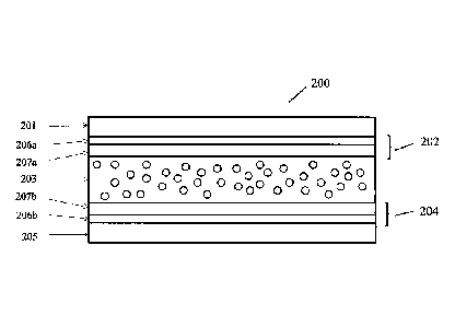
device. The use of
curved and dynamically flexing substrates enables flexible and stretchable
applications for
electrochromic films. Furthermore, the nonreactive and impermeable nature of
graphene
increases the durability of the device through increased resistance to
external impurities. In
addition, the incorporation of ferroelectric materials allows the device to
exhibit nonvolatile
usage; that is, devices can remain transparent with no external power source.
Furthermore,
Date Recue/Date Received 2021-04-06
CA 02929872 2016-05-05
WO 2015/069188
PCT/SG2014/000522
- 2 -
devices may exhibit a charging effect, permitting recovery of energy stored in
alignment of
ferroelectric dipoles within the ferroelectric material.
[0004] In accordance with one version of the invention, there is provided
an
electrochromic device. The device comprises at least one electrode including
graphene and
at least one ferroelectric material; and an active layer.
[0005] In further, related versions, the at least one electrode may
comprise two
electrodes, each of the two electrodes including graphene and at least one
ferroelectric
material. The at least one electrode may comprise at least one ferroelectric
material layer
located between a first layer of graphene and a second layer of graphene. The
at least one
electrode may comprise two electrodes, a first electrode of the two electrodes
including
graphene and at least one ferroelectric material, and a second electrode of
the two electrodes
comprising only graphene. The active layer may comprise a liquid crystal
material, such as
4-Cyano-4'-pentylbiphenyl. The active layer may comprise the liquid crystal
material
dispersed in a polymer, such as poly(methyl methacrylate), poly(vinyl alcohol)
or
poly(vinyl butyral). The active layer may comprise a suspending polymer
material, and
may include particles, such as dihydrocinchonidine bisulfite polyiodide
particles, in a
suspending fluid, such as an oligomeric ester of methacrylic acid. The
ferroelectric material
may comprise a ferroelectric polymer, such as a fluoropolymer ferroelectric
material or co-
fluoropolymer ferroelectric material, for example polyvinylidene fluoride or
polyvinylidene
fluoride co-trifluoroethylene. The ferroelectric material may comprise an
inorganic
material, such as lead zirconate titanate.
[0006] In further, related versions, the electrochromic device may comprise
a
nonvolatile electric field across the active layer such that the
electrochromic device is
configured to remain transparent with no external power source. The
electrochromic device
may be configured to permit recovery of energy stored in alignment of
ferroelectric dipoles
within the ferroelectric material. The graphene of the at least one electrode
may comprise
monolayer graphene, bi-layer graphene, multilayer graphene, an interconnected
graphene-
based mesh network or a graphene composite. The electrochromic device may
further
comprise a substrate, which may be a flexible substrate, such as polyethylene
terephthalate
or polyvinylidene fluoride co-trifluoroethylene, or may be a rigid substrate,
such as glass.
The electrochromic device may be flexible and/or stretchable. The substrate
may comprise
at least one of an air gap and a thermal insulator between at least two layers
of the substrate.
CA 02929872 2016-05-05
WO 2015/069188
PCT/SG2014/000522
- 3 -
The active layer may comprise at least one dye molecule. The device may
comprise only
one substrate, where a surface of the device comprises graphene; or the device
may
comprise two substrates. At least one substrate of the two substrates may
comprise a
second active layer, a photovoltaic cell and/or a light-emitting diode.
[0007] In further, related versions, the electrochromic device may comprise
at least a
portion of: a window, a sunroof, an electronic paper display, an electronic
reader, an
adjustable light diffuser, a privacy screen, a curtain, a textile, a wearable
item of apparel or
a projection screen. The device may comprise at least a portion of a
photovoltaic device or
an organic light-emitting display.
[0008] In another version of the invention, there is provided a method of
manufacturing
an electrochromic device. The method comprises: forming at least one layer
comprising
= graphene; forming at least one layer comprising a ferroelectric material
to be coupled to the
at least one layer comprising graphene, thereby forming at least one electrode
of the
electrochromic device; and forming at least one layer comprising an active
material
configured such that the at least one electrode can generate an electric field
across the at
least one layer comprising the active material.
[0009] In further, related versions, forming the at least one layer
comprising graphene
may comprise a process from the group consisting of: chemical vapor deposition
(CVD),
micromechanical exfoliation, liquid-phase epitaxy, printing, reduction of
graphene oxide,
unzipping of carbon nanotubes and epitaxial growth. Forming the at least one
layer
comprising graphene may comprise growing graphene directly on a substrate, or
growing
graphene on a substrate and subsequently transferring the graphene off the
substrate.
Forming the at least one layer comprising a ferroelectric material may
comprise growing a
polymeric ferroelectric material on the graphene, the growing the polymeric
ferroelectric
material comprising a process from the group consisting of: spin-coating, dip-
coating, wire
wound bar coating, blade coating, drop casting, Langmuir-Blodgett film growth,
and
extrusion from melt. Forming the at least one layer comprising an active
material may
comprise dispersing a suspended polymer material within a fluid layer, thereby
forming a
suspended polymer fluid, and depositing the suspended polymer fluid on the at
least one
electrode. Depositing the suspended polymer fluid may comprise a process from
the group
consisting of: drop casting, spray coating, spin coating, capillary filling,
wire wound bar
coating, dip-coating and blade coating. Forming the at least one layer
comprising an active
CA 02929872 2016-05-05
WO 2015/069188
PCT/SG2014/000522
- 4 -
material may comprise growing a polymer dispersed liquid crystal structure by
at least one
of: drop casting, spin coating, spray coating, printing, capillary filling,
wire wound bar
coating, dip-coating and blade coating. Forming the at least one layer
comprising an active
material may comprise growing a layered liquid crystal structure by at least
one of: drop
casting, spin coating, spray coating, capillary filling, wire wound bar
coating, dip-coating
and blade coating. The method may further comprise infiltrating the at least
one layer
comprising an active material with dye molecules.
BRIEF DESCRIPTION OF THE DRAWINGS
[0010] The foregoing will be apparent from the following more particular
description of
example embodiments of the invention, as illustrated in the accompanying
drawings in
which like reference characters refer to the same parts throughout the
different views. The
drawings are not necessarily to scale, emphasis instead being placed upon
illustrating
embodiments of the present invention.
[0011] FIG. 1 is a schematic diagram of the structure of an electrochromic
device, in
accordance with the prior art.
[0012] FIG. 2 is a schematic diagram of an electrochromic device utilizing
two
graphene-ferroelectric electrodes, in accordance with a version of the
invention.
[0013] FIG. 3 is a schematic diagram of an electrochromic device utilizing
one
graphene-ferroelectric electrode and one graphene electrode, in accordance
with a version
of the invention.
[0014] FIG. 4 is a schematic diagram of an electrochromic device utilizing
graphene-
ferroelectric sandwiched electrodes, in accordance with a version of the
invention.
[0015] FIG. 5 is a schematic diagram of a substrate of an electrochromic
device,
incorporating an air gap or thermal insulator, in accordance with a version of
the invention.
[0016] FIG. 6 is a schematic diagram of operation of an electrochromic
device in
accordance with a version of the invention, in the OFF mode, with no
orientation of the
ferroelectric dipoles.
[0017] FIG. 7 is a schematic diagram of operation of an electrochromic
device in
accordance with a version of the invention, in the ON mode, with ferroelectric
dipoles
aligned with the external field.
CA 02929872 2016-05-05
WO 2015/069188
PCT/SG2014/000522
- 5 -
[0018] FIG. 8 is a schematic diagram of operation of an electrochromic
device in
accordance with a version of the invention, once the external field is
removed, with particle
alignment maintained due to remnant field within the ferro electric layer.
[0019] FIGS. 9A and 9B are photographs showing the-operation (OFF in FIG.
9A, ON
in FIG. 9B) of a device utilizing graphene-femelectric electrodes, in
accordance with a
version of the invention.
[0020] FIG. 10 is a graph of transparency as a function of applied voltage
in
electrochromic devices in an experiment, in accordance with a version of the
invention.
DETAILED DESCRIPTION OF THE INVENTION
[0021] A description of example embodiments of the invention follows.
[0022] In accordance with a version of the invention, graphene and
ferroelectrics are
incorporated within the field of electrochromic technologies for films with
tunable
transparency levels. Processes required for manufacturing said films are
provided.
Ferroelectricity introduces a degree of non-volatile control to films with
regards to their
transparency and ergo power consumption. Films may be used for a variety of
applications
including but not limited to smart windows, heat reduction windows,
electrochromic
privacy screens, electrochromic curtains, adjustable light diffusers for
domestic and
commercial lighting, adjustable light diffusers for camera flashes, wearable
electrochromic
apparel, projection screens, solar cells, organic light-emitting displays
(OLEDs), electronic
readers, as well as flexible variants of aforementioned versions. Films may be
tinted using
dichroic or pleochroic dyes for coloration.
[0023] In accordance with a version of the invention, graphene plus
ferroelectric
polymers are used as a replacement for Indium Tin Oxide (ITO) as the
transparent electrode
material in an electrochromic device. Graphene's flexibility no longer limits
the substrate to
glass, and the use of curved and dynamically flexing substrates enable
flexible and
stretchable applications for electrochromic films. Furthermore, the
nonreactive and
impermeable nature of graphene increases the durability of the device through
increased
resistance to external impurities.
[0024] In accordance with a version of the invention, the incorporation of
ferro electric
materials allows the device to exhibit nonvolatile usage; that is, devices can
remain
transparent with no external power source. Furthermore, devices may exhibit a
charging
CA 02929872 2016-05-05
WO 2015/069188
PCT/SG2014/000522
- 6 -
effect, allowing energy dissipated within the device during the initial 'ON'
state to be
recovered once the device is turned 'OFF'. These features allow the
electrochromic device
to be more energy efficient when compared to existing commercially available
devices.
Ferroelectric polymers are also known to reduce the sheet resistance of
graphene, further
improving the power consumption of these devices. When fluoropolymer
ferroelectrics are
utilized the superhydrophobic property of the composite imparts a self-
cleaning
functionality to the device.
[0025] The terms "electrochromic device" and "electrochromic panel," as
they are used
herein include, but are not limited to, the following device or panel
structures: suspended
particle devices (SPD), polymer dispersed liquid crystal (PDLC) or layered
liquid crystal
(LLC) structures. Such devices switch between opaque and transparent states
via the
application of an electric field between two transparent electrical
conductors. The active
layer sandwiched between the conductors is responsible for the optical
switching observed.
[0026] FIG. 1 is a schematic diagram of the structure of an electrochromic
device 100,
in accordance with the prior art. The device 100 includes a substrate 101, a
transparent
conductor 102, an active layer 103, a second transparent conductor 104 and a
second
substrate 105. The two transparent conductors 102 and 104 act as electrodes.
- Commercially available electrochromic devices currently utilize Indium
Tin Oxide (ITO) as
the transparent conductors 102 and 104. These devices require between 2 and 10
Watts of
uninterrupted power per square meter of panel area in order to maintain a
transparent state.
Power is typically dissipated while the device is in operation and cannot be
recovered when
the device is turned off. Furthermore, the devices are inflexible, limiting
the range of
structures on which they can be applied. In contrast, a version in accordance
with the
present invention aims to rectify the shortcomings of existing electrochromic
devices
mentioned above by making use of Graphene-Ferroelectric composite electrodes
as a
replacement for Indium Tin Oxide (ITO) electrodes.
[0027] In accordance with a version of the invention, ferroelectric
materials are capable
of lowering the sheet resistance of graphene, in turn lowering resistive
losses and thus
power consumption of devices that utilize electrodes with such structures.
Electrodes
fashioned out of graphene-ferroelectric composite materials can also be
flexible without
deteriorating electrical performance. In such cases the inclusion of
ferroelectric materials
may protect the graphene from structural damage during flexing. The
ferroelectric also
CA 02929872 2016-05-05
WO 2015/069188 PCT/SG2014/000522
- 7 -
increases the longevity of the device by protecting it from failures due to
short circuits
through the active layer. Most importantly, upon application of an external
field the
ferroelectric layer may polarize, and the resultant realignment of dipoles
within the
ferroelectric layer will generate a nonvolatile electric field across the
active layer. It is
expected that this nonvolatile field may enable devices that are able to
operate, i.e., remain
transparent, without the need for a continuous power supply, thereby further
lowering
power consumption. Additionally, the remnant energy stored due to the
alignment of the
dipoles may be recoverable when switching the device back to its opaque state.
[0028] FIG. 2 is a schematic diagram of an electrochromic device 200, such
as an
electrochromic panel, which utilizes two graphene-ferroelectric electrodes, in
accordance
with a version of the invention. The device 200 includes a substrate 201, a
first electrode
202, an active layer 203, a second electrode 204 and a second substrate 205.
Each of the
electrodes 202 and 204 includes two layers: a graphene layer 206a/206b, and a
ferroelectric
layer 207a/207b.
[0029] FIG, 3 is a schematic diagram of an electrochromic device 300
utilizing one
graphene-ferroelectric electrode and one graphene-only electrode, in
accordance with a
version of the invention. In this version, the device 300 includes a substrate
301, a first
electrode 302, an active layer 303, a second electrode 304 and a second
substrate 305.
Whereas, the first electrode 302 includes two layers, i.e., a graphene layer
306a and a
ferroelectric layer 307a, the second electrode is a graphene-only layer 306b.
[0030] FIG. 4 is a schematic diagram of an electrochromic device utilizing
graphene-
ferroelectric sandwiched electrodes, in accordance with a version of the
invention. Such a
structure allows greater control over the polarization of the ferroelectric
layers. The device
400 includes a substrate 401, a first electrode 402, an active layer 403, a
second electrode
404 and a second substrate 405. Each of the electrodes 402 and 404 includes
three layers:
two graphene layers 406a/406b are positioned on either side of a ferroelectric
layer 407a,
and in the other electrode, two graphene layers 406c/406d are positioned on
either side of a
ferroelectric layer 407b.
[0031] FIG. 5 is a schematic diagram of a substrate 501 of an
electrochromic device,
. incorporating an air gap or thermal insulator, in accordance with a version
of the invention.
In this version, it can be seen that the substrate 501 (shown here in
isolation from the rest of
the electrochromic device, such as that of FIGS. 2-4), may feature an air gap
or thermal
CA 02929872 2016-05-05
WO 2015/069188
PCT/SG2014/000522
- 8 -
insulator in area 508, which is interposed between two substrate layers
501a/501b. Such an
air gap or thermal insulator 508 may assist with thermal stability of the
device.
[0032] Below there are provided three separate sections, each relating to
either one of a)
manufacturing processes and description of materials used in the graphene-
ferroelectric
electrodes, b) manufacturing processes and description of materials used in
the active layer
or c) methods for assembling the device and preferred modes of operation, in
accordance
with a version of the invention.
[0033]
[0034] a) Manufacturing processes and description of materials used in
Graphene-
ferroelectric electrodes
[0035]
[0036] In accordance with a version of the invention, benefits in device
performance
and efficiency arise from the specific usage and construction of the graphene-
ferroelectric
electrodes. As used herein, the use of the term "graphene" can refer to mono-
layer, bi-layer
or multilayer graphene, as well as to interconnected graphene-based mesh
networks such as
graphene foam. The production process for such graphene can include but are
not limited to:
chemical vapor deposition (CVD), micromechanical exfoliation, liquid-phase
epitaxy,
printing, reduction of graphene oxide, unzipping of carbon nanotubes,
epitaxial growth on
silicon carbide and others. In some cases, graphene composites can be used.
[0037] In accordance with a version of the invention, in the context of
growth-based
processes, graphene may be directly grown on the substrate or can be
transferred from the
substrate that the graphene is originally grown on. The substrate may be
either flexible in
nature, such as the polymer polyethylene terephthalate (PET) or the
ferroelectric
polyvinylidene fluoride co-trifluoroethylene (PVDF-TrFE), or rigid, such as
glass. The
second substrate may also be another active layer or device such as a
photovoltaic cell or an
organic light-emitting diode. In some cases there may not be a second
substrate and the
graphene surface of the device may be exposed. If additional thermal isolation
is desired,
each substrate may consist of two sheets of either a flexible or rigid
material with an air gap
or thermal insulator in between (as shown in FIG. 5, above).
[0038] In accordance with a version of the invention, the ferroelectric
layer may utilize
polymer materials including but not limited to fluoropolymers and co-
fluoropolymers such
as polyvinylidene fluoride (PVDF) and polyvinylidene fluoride co-
trifluoroethylene
CA 02929872 2016-05-05
WO 2015/069188
PCT/SG2014/000522
- 9 -
(PVDF-TrFE), or inorganic compounds such as lead zirconate titanate (PZT). In
a version
pertaining to the use of polymeric ferroelectrics, the layers may be grown on
the graphene
substrates either before or after the transfer process, using processes
including but not
limited to: spin-coating, dip-coating, wire wound bar coating, blade coating,
drop casting,
Langmuir-Blodgett (LB) film growth or extrusion from melt. The composite
structure
described herein is also referred to herein as a graphene ferroelectric
electrode.
[0039]
[0040] b) Manufacturing processes and description of materials used in the
active layer
[0041]
[0042] In accordance with a version of the invention, the active layer may
consist of
varying structures depending on the nature of technology utilized for the
electrochromic
film ¨ namely, suspended particle devices (SPDs), polymer dispersed liquid
crystals
(PDLCs) or layered liquid crystal (LLC) structures.
[0043] In the case of SPDs, in accordance with a version of the invention,
the active
layer consists of a suspending polymer material in either an organic or
inorganic fluid. The
suspending polymer material may be polarizing at a molecular level and consist
of particles
such as herapathite, (dihydrocinchonidine bisulfite polyiodide) or others. The
suspending
fluid may comprise of an organic liquid or gel such as an oligomeric ester of
methacrylic
acid. Suspended polymer material can be dispersed within the fluid layer by a
mixing
process and deposited on electrodes by drop casting, spray coating, spin
coating, capillary
filling, wire wound bar coating, dip-coating, blade coating, or others.
[0044] In the case of the device consisting of a PDLC structure, in
accordance with a
version of the invention, the active layer consists of liquid crystal
materials, such as 4-
Cyano-4'-pentylbiphenyl (5CB), in a polymeric matrix, such as poly(methyl
methacrylate),
poly(vinyl alcohol), poly(vinyl butyral) or others. Materials can be dissolved
in a common
solvent and later separated using either one of polymerization induced phase
separation
(PIPS), thermally induced phase separation (TIPS), solvent induced phase
separation
(SIPS), or others. The active layer can be assembled either directly on the
electrode or on a
different substrate and later transferred. Growth processes include but are
not limited to:
drop casting, spin coating, spray coating, printing, capillary filling, wire
wound bar coating,
dip-coating, blade coating, or others. Where active layers are grown directly
on the surface
of the graphene-ferroelectric electrode and an organic ferroelectric is used,
the film may be
CA 02929872 2016-05-05
WO 2015/069188
PCT/SG2014/000522
- 10 -
more uniform due to improved surface attraction / wetting. Instead of
comprising of
separate ferroelectric and active layers in a polymer dispersed liquid crystal
(PDLC)
structure, the material used for encapsulating the liquid crystal can itself
be ferroelectric.
Thus, it will be appreciated that, as used herein, a ferroelectric material
may comprise at
least a portion of an active layer, while the active layer may include the
ferroelectric
material; that is, the ferroelectric material of the electrode need not be in
an entirely separate
layer from the active layer.
[0045] In the case of LLC devices, in accordance with a version of the
invention, the
active layer consists of solely liquid crystal materials such as 4-Cyano-4'-
pentylbiphenyl
(5CB) encapsulated between two graphene-ferroelectric electrodes. The active
layer can be
sealed using a sealant such as acryl, or others, to prevent leakage. Examples
of deposition
process that may be used include but are not limited to: drop casting, spin
coating, spray
coating, capillary filling, wire wound bar coating, dip-coating, blade
coating, or others.
[0046] In accordance with a version of the invention, the active layer may
also be
infiltrated with dichroic or pleochroic dye molecules that may or may not be
of azo or
anthraquinone type, which allow the device to be colored in its opaque state.
In such
instances, the device switches between a colored and a transparent condition
in its OFF and
ON state respectively.
[0047]
[0048] c) Methods for assembling the device and preferred modes of
operation
[0049]
[0050] In accordance with a version of the invention, assembly of the final
device
consists of joining/interfacing the products discussed in parts a) and b)
above. More
specifically, the active layers described in part b) can be either directly
grown on the
ferroelectric surface of one or both graphene-ferroelectric electrode
structures described in
a) using methods described in part b) and then these electrodes assembled, or
can be grown
separately using methods described in part b) and later assembled to the
ferroelectric surface
of the graphene-ferroelectric electrodes. Methods for the assembly include but
are not
limited to: direct contacting, heat based lamination, lamination with the
assistance of an
optically clear adhesive, or others.
[0051]
CA 02929872 2016-05-05
WO 2015/069188
PCT/SG2014/000522
- 11 -
[0052] Regarding the operation of devices, in accordance with a version of
the
invention, electrical contacts can be connected to either an alternating
current (AC) or direct
current (DC) source. On application of an electric field, the (initially)
randomly oriented
molecules within the active layer align with the field, allowing light to pass
through without
scattering. Visually, this is apparent as a switching between opaque and
transparent states.
[0053] Without wishing to be bound by theory, it is expected that under the
application
of a direct current source, the scattered dipoles of the ferroelectric layer
shall align with the
electric field, resulting in a nonvolatile electric field throughout the
active layer. This is
analogous to the operation of a parallel plate capacitor. Once the external
source has been
removed, the nonvolatile field within the ferroelectric may remain, the
magnitude of which
can be estimated as below.
[0054] Prior to estimating the magnitude of the nonvolatile field, the
voltage drop across
the ferroelectric layer or layers needs to be calculated, in order to confirm
whether the
ferroelectric can be polarized. In order to do so, the system can be modeled
as dielectrics in
series, with the relative parameters being the dielectric constants and
thicknesses of both the
active and ferroelectric layers. For one version of the invention, in which
the ferroelectric
layer comprises of PVDF-TrFE (relative dielectric constant of 10.12) and the
active layer
consists of a PMMA matrix with liquid crystals (relative dielectric constant
measured to be
13.5), the voltage dropped across the ferroelectric for a 200V external bias
is calculated as:
[0055]
[0056] V = V041+(cF*tAL)I(gAL*tp)] =-- 80.23V
[0057]
[0058] where cF, and EAL are the relative dielectric constants of the
ferroelectric and
active layers respectively, tF and tAL are the relative thicknesses of the
ferroelectric and
active layers respectively, and Vo is the 200V applied DC voltage. The
thicknesses of the
ferroelectric and active layers have been assumed to be 800nm and 1.6 m
respectively.
Using this thickness, the voltage across the ferroelectric thus corresponds to
an electric field
of 100.29V/1.1m, which is higher than the 100V/ m required to polarize it.
[0059] In accordance with a version of the invention, it has been found
that the typical
charge carrier density that can be introduced to the surface of the graphene
due to
ferroelectric doping, assuming that the ferroelectric material is PVDF-TrFE
and that the
ferroelectric has been completely polarized, is n = 4x10¹³/cm2. Treating the
system as a
CA 02929872 2016-05-05
WO 2015/069188
PCT/SG2014/000522
- 12 -
parallel plate capacitor, the nonvolatile field due to these charge carriers
can be obtained
using:
[0060]
[0061] E = Q/cA = nq/c
[0062]
[0063] where E is the electric field that remains when the power is
switched off, n is the
charge carrier density on each plate, q is the electron charge and c is the
dielectric constant
of the active layer. For one version of the invention, in which the active
layer comprises of a
PMMA matrix embedded with liquid crystals, the dielectric constant has been
measured to
be 1.2x10⁻¹⁰F/m. Using this, the field across the active layer can be
calculated to be
53V/pm.
[0064] As typical electrochromic panels require greater than 2V/pm in order
to switch
ON, it is expected that the nonvolatile field shall allow the particles within
the active layer
to remain in an aligned (i.e. transparent) state without an external power
supply. An
illustration of the process is provided in FIGS. 6, 7 and 8.
[0065] FIG. 6 is a schematic diagram of operation of an electrochromic
device in
accordance with a version of the invention, in the OFF mode, with no
orientation of the
ferroelectric dipoles 609.
[0066] FIG. 7 is a schematic diagram of operation of an electrochromic
device in
accordance with a version of the invention, in the ON mode, with ferroelectric
dipoles 709
aligned with the external field.
[0067] FIG. 8 is a schematic diagram of operation of an electrochromic
device in
accordance with a version of the invention, once the external field is
removed, with particle
alignment 810 maintained due to remnant field 811 within the ferroelectric
layer.
[0068] In accordance with a version of the invention, the opaque state of
the device may
be re-obtained by forcing the dipoles within the ferroelectric to return to
their original
scattered alignment. The energy stored in the alignment of the ferroelectric
dipoles may be
recovered and used to power other devices or stored and used in subsequent
operations of
the same device.
[0069] FIGS. 9A and 9B are photographs showing the operation (OFF in FIG.
9A, ON
in FIG. 9B) of a prototype device utilizing graphene-ferroelectric electrodes,
in accordance
CA 02929872 2016-05-05
WO 2015/069188
PCT/SG2014/000522
- 13 -
with a version of the invention. The device is a PDLC structure with two
graphene-
ferroelectric electrodes. The size of the device is approximately 5cm by 5cm.
[0070] The expected benefits of graphene-ferroelectric electrochromic
devices in
accordance with a version of the invention, as compared with commercially
available
devices, include the following:
[0071] Battery effect: Commercial devices require continuous power in order
to remain
transparent. In contrast, the ability of the ferroelectric layer to be
polarized, permits
graphene-ferroelectric electrochromic devices to operate without external
power, once the
ferroelectric layer has been charged. The charging / discharging of the
ferroelectric may
also allow the device to store and recover the energy used to switch between
the transparent
and opaque states.
[0072] Lower power consumption: The theoretical limit for the sheet
resistance of
graphene doped with ferroelectric materials is less than its ITO counterpart,
hence power
lost due to resistive losses at the electrodes should be less with graphene-
ferroelectric
devices. This will result in an increase in energy efficiency as compared to
standard devices.
[0073] Self-cleaning: In the instance where the graphene-ferroelectric
electrode is
exposed to air, the superhydrophobic nature of these materials enables devices
to be highly
repellant to dust and other sources of contamination.
[0074] Flexibility: Commercially available devices typically make use of
Indium Tin
Oxide (ITO) as the electrode. The replacement of ITO with graphene-
ferroelectric
electrodes allows devices to be flexible.
[0075] Increased device lifetime: The ferroelectric layer may increase the
life of the
device by protecting it from short circuits between the two conducting
graphene sheets as
the active layer degrades over time.
[0076] Thermal stability: As a result of graphene's high thermal
conductivity, the
graphene-ferroelectric electrodes based devices will dissipate localized point
thermal
sources better than their ITO counterparts and will protect the device from
degradation
making device operation more reliable.
[0077]
[0078] Industrial applications of an electrochromic device in accordance
with a version
of the invention include, but are not limited to:
CA 02929872 2016-05-05
WO 2015/069188 PCT/SG2014/000522
- 14 -
[0079] -As-built or retrofitted electrochromic panels for windows in
residential /
commercial buildings
[0080] -As-built or retrofitted electrochromic panels for windshields,
windows and
sunroofs for automobiles
[0081] -Flexible black-and-white or color displays for use as electronic
paper either
standalone or in electronic readers
[0082] -Adjustable diffusers for residential and commercial lighting
installations
[0083] -Adjustable diffusers for camera flashes
[0084] -Heat reduction windows
[0085] -Privacy screens
[0086] -Flexible electrochromic textiles for curtains, lampshades,
furniture and
coverings etc.
[0087] -Wearable electrochromic apparel
[0088] -Projection screens
[0089] -Integrated with photovoltaic devices
[0090] -Organic light-emitting displays (OLEDs)
[0091]
[0092] Table 1 is a comparison of a prior art panel with an electrochromic
panel in
accordance with a version of the invention.
Table 1
Prior Art Prototype
Metric Commercial Flexible Privacy Glass, Ferroelectric
Electrochromic Model
Panel
Power Consumption 6000 3.5
(mW/sqm)
Transparency ON state 75 > 75
(%)
= Transparency OFF state 7 0.5
cyo
UV Transmission (at 1% 0.1%
CA 02929872 2016-05-05
WO 2015/069188
PCT/SG2014/000522
- 15 -
250 nm)
Controlled dimming No Tunable Opacity
Non-volatile operation No Yes
Flexibility Twice as flexible as Completely flexible
glass
[0093]
[0094] It can be seen in Table 1 that a version of the invention has a
lower power
consumption (on the order of 0.5% of control); a higher contrast ratio; and is
on the order of
100 times more flexible than glass. Initial non-volatile operation testing
shows a delay of 2-
3 seconds in return to 'OFF' state for the graphene-ferroelectric electrode.
Tunable opacity
has been demonstrated.
[0095] FIG. 10 is a graph of transparency as a function of applied voltage
in
electrochromic devices in an experiment, in accordance with a version of the
invention. In
the experiment, a UV-Vis spectrometer was set to 550 nm (green light). It can
be seen that
transparency varies with applied voltage. The demonstration was performed on a
thinner
active layer on a low quality substrate, and thus had unoptimized transparency
levels.
[0096] While this invention has been particularly shown and described with
references
to example embodiments thereof, it will be understood by those skilled in the
art that
various changes in form and details may be made therein without departing from
the scope
of the invention encompassed by the appended claims.