Note : Les descriptions sont présentées dans la langue officielle dans laquelle elles ont été soumises.
CA 02931399 2016-05-20
WO 2015/077472
PCT/US2014/066657
SAGNAC LOOP MIRROR BASED LASER CAVITY ON SILICON PHOTONICS
PLATFORM
CROSS-REFERENCE TO RELATED APPLICATIONS
[0001] This application claims priority to and the benefit of co-pending
U.S.
provisional patent application Serial No. 61/906,529, filed November 20, 2013,
which
application is incorporated herein by reference in its entirety.
FIELD OF THE INVENTION
[0002] The invention relates to optical cavities in general and
particularly to an optical
cavity that can be used with lasers.
BACKGROUND OF THE INVENTION
[0003] Semiconductor lasers and optical amplifiers are preferred in
transceivers
because they are efficiently electrically pumped and the die size is small.
Lasing is a radiative
recombination process in semiconductors, where an electron in the conduction
recombines
with a hole in the valance band and a photon is emitted. The reverse process
is electron hole
pair generation through optical absorption, as occurs in such devices as
photodetectors and
solar cells.
[0004] Silicon photonics is widely seen as an enabling technology to
address the
exponentially increasing demand for data communication bandwidth. Lasers are
critical
components in data transmission systems. Two fundamental elements for a laser
are its gain
medium and resonating cavity. Due to the indirect bandgap of silicon, several
approaches of
introducing gain medium into the photonic integration material system has been
reported,
including edge coupled bonding (see, for example A. J. Zilkie, P. Seddighian,
B. J. Bijlani, W.
Qian, D. C. Lee, S. Fathololoumi, J. Fong, R. Shafiiha, D. Feng, B. J. Luff,
X. Zheng, J. E.
Cunningham, A. V. Krishnamoorthy, and M. Asghari, "Power-efficient III-
V/Silicon external
cavity DBR lasers," Optics Express, Vol. 20, pp. 23456-23462, 2012; S. Tanaka,
S. H. Jeong,
S. S., T. Kurahashi, Y. Tanaka, and K. Morito, "High-output-power, single-
wavelength silicon
hybrid laser using precise flip-chip bonding technology," Optics Express, Vol.
20, pp. 28057-
1
CA 02931399 2016-05-20
WO 2015/077472
PCT/US2014/066657
28069, 2012), direct bonding (see, for example A. W. Fang, H. Park, 0. Cohen,
R. Jones, M. J.
Paniccia, and J. E. Bowers, "Electrically pumped hybrid AlGaInAs-silicon
evanescent laser,"
Optics Express, Vol. 14, pp. 9203-9210, 2006; S. Keyvaninia, G. Roelkens, D.
Van Thourhout,
C. Jany, M. Lamponi, A. Le Liepvre, F. Lelarge, D. Make, G. H. Duan, D.
Bordel, and J. M.
Fedeli, "Demonstration of a heterogeneously integrated III-V/SOI single
wavelength tunable
laser," Optics Express, Vol. 21, pp. 3784-3792, 2012; T. Creazzo, E. Marchena,
S. B.
Krasulick, P. Yu, D. Van Orden, J. Y. Spann, C. C. Blivin, L. He, H. Cai, J.
M. Dallesasse, R.
J. Stone, and A. Mizrahi, "Integrated tunable CMOS laser," Optics Express,
Vol. 21, pp.
28048-28053, 2013), heavily N-doped germanium (see, for example R. E. Camacho-
Aguilera,
Y. Cai, N. Patel, J. T. Bessette, M. Romagnoli, L. C. Kimerling, and J.
Michel, "An electrically
pumped germanium laser," Optics Express, Vol. 20, pp. 11316-11320, 2012), and
quantum dot
structures (see, for example T. Wang, H. Liu, A. Lee, F. Pozzi, and A. Seeds,
"1.3- m
InAs/GaAs quantum-dot lasers monolithically grown on Si substrates," Optics
Express, Vol.
19, Issue 12, pp. 11381-11386 (2011)). Laser cavities are usually built using
Distributed Bragg
Reflectors (DBRs), or DBRs together with ring resonator filters, which require
high
lithography resolution and are sensitive to fabrication variations.
[0005] Conservation of both energy and momentum are required in the lasing
process.
Energy conservation is satisfied because the emitted photon's energy is equal
to the bandgap of
the semiconductor. However, a photon's momentum is negligible compared to that
of an
electron or a hole. To meet the momentum conservation requirement, the top of
the valence
band and the bottom of the conduction band need to be aligned. In other words,
the
semiconductor needs to be a direct bandgap material. A number of III-V
compound materials
such as gallium arsenide (GaAs) and indium phosphide (InP) are direct bandgap
semiconductors. However, silicon is an indirect bandgap semiconductor.
[0006] Raman silicon lasers have been demonstrated. Making an electrically
pumped
silicon laser is prohibitively difficult. Another gain material has to be
introduced into the
silicon material system in which laser action is desired. Various gain
integration approaches
have been reported, including monolithic epitaxy, wafer bonding, and SOA edge
coupling.
[0007] X. Shu, S. Jiang, and D. Huang, "Fiber grating Sagnac loop and its
multiwavelength-laser application, "IEEE Photonics Technology Letters, Vol.
12, pp. 980-
2
CA 02931399 2016-05-20
WO 2015/077472
PCT/US2014/066657
982, 2000 is said to describe a novel simple comb filter, which is based on a
Sagnac
interferometer with a fiber Bragg grating asymmetrically located in its fiber
loop. The filter
has advantages of simple design and easy fabrication, low insertion loss and
low cost. Two
filters with triple bandpasses and dual bandpasses, respectively, were
fabricated and applied to
an erbium-doped fiber ring laser. Stable triple-wavelength and dual-wavelength
laser
operations have been demonstrated.
[0008] J. Zhou, P. Yan, H. Zhang, D. Wang, and M. Gong, "All-fiber mode-
locked ring
laser with a Sagnac filter," IEEE Photonics Technology Letters, Vol. 23, pp.
1301-1303, 2011
is said to describe the following: Terbium-doped mode-locked fiber lasers are
versatile sources
of femtosecond pulses. The development of new pulse-shaping mechanisms in
fiber lasers
allows the generation of higher energy femtosecond pulses than the soliton
mode-locked lasers
which are required in the application. However the pulses from Yb-doped mode-
locked fiber
lasers are longer in width than the soliton pulses due to the normal
dispersion of the fiber. Thus
grating pairs are necessary in and out of the cavity to provide negative
dispersion. An All-
Normal-Dispersion (ANDi) Yb-doped fiber laser has been demonstrated with a
spectral filter
instead of the grating pair in the cavity. The spectral filtering of a highly-
chirped pulse in the
laser cavity is the key component of the pulse shaping in this type of mode-
locked laser. The
influence of the bandwidth of the filter on the mode-locking has been
theoretically
investigated. The bulk interference or birefringent filter is commonly used as
the spectral filter.
In order to develop the all-fiber configuration free from misalignment some
fiber-type filters
have been investigated. Recently an all-fiber Lyot filter with a section of
Polarization
Maintaining (PM) fiber has been used as the spectral filter in ANDi laser and
240 fs dechirped
pulses were obtained. According to the discussion in [2], [3] the duration of
the mode locked
pulse diminishes with the decrease of the filtering bandwidth until the mode-
locking fails. The
Lyot filter can be used as a bandwidth-tunable filter as the bandwidth depends
on the length of
the PM fiber. However the modulation depth of the Lyot filter is dominated by
the Polarization
Controllers (PCs).
[0009] There is a need for an improved external cavity for use with lasers.
3
CA 02931399 2016-05-20
WO 2015/077472
PCT/US2014/066657
SUMMARY OF THE INVENTION
[0010] According to one aspect, the invention features an optical cavity.
The
optical cavity comprises a single optical port configured to provide an
optical output beam; a
first mirror element comprising a submicron silicon waveguide, the first
mirror element having
a first transmittance and a first reflectivity, the first mirror element
forming a first optical
reflector situated at a first end of the optical cavity, the first mirror
element in optical
communication with the single optical port; a second mirror element having a
second
transmittance and a second reflectivity, the second mirror element forming a
second optical
reflector situated at a second end of the optical cavity, at least one of the
first mirror element
and the second mirror element is a Sagnac loop mirror; and situated in serial
optical
communication between the first mirror element and the second mirror element:
a filter
element configured to pass an optical beam having a selected optical
wavelength therethrough;
and a gain cavity configured to contain therein an optical gain medium.
[0011] In another embodiment, the first mirror element is a broadband
reflector.
[0012] In yet another embodiment, the first mirror element has a
reflectivity that
increases as the selected wavelength is increased.
[0013] In another embodiment, the first mirror element has a variable
reflectivity.
[0014] In still another embodiment, the filter element is a micro-ring
based filter.
[0015] In a further embodiment, the filter element is a tunable filter.
[0016] In yet a further embodiment, the filter element is a thermally
tunable filter.
[0017] In an additional embodiment, the filter element has multiple pass
bands.
[0018] In one more embodiment, the second mirror has a reflectivity defined
by a facet.
[0019] In still a further embodiment, the selected optical wavelength is a
wavelength
situated within a wavelength range used in telecommunication.
[0020] In one embodiment, the selected optical wavelength is a wavelength
situated
within the 0-Band.
[0021] In yet another embodiment, the selected optical wavelength is a
wavelength
situated within the C-Band.
[0022] In still another embodiment, the selected optical wavelength is a
wavelength
situated within a band selected from the e-Band, the S-Band, the L-Band and
the U-Band.
4
CA 02931399 2016-05-20
WO 2015/077472
PCT/US2014/066657
[0023] In yet a further embodiment, the optical gain medium is optically
coupled to the
optical cavity via at least one of a butt-coupler, a taper, an inverse taper,
a lens, and a lens
array.
[0024] In an additional embodiment, the optical cavity is configured to be
operated
without cooling.
[0025] In one more embodiment, the optical cavity is configured to be
operated without
hermetic sealing. However, it is to be understood that an individual die may
comprise hermetic
sealing.
[0026] In still a further embodiment, the facet comprises an optical
coating.
[0027] In another embodiment, the optical output beam comprises a single
optical
wavelength of interest.
[0028] In yet another embodiment, the optical output beam comprises a
plurality of
optical wavelengths of interest.
[0029] In still another embodiment, the optical output beam comprises a
narrow
linewidth optical output beam.
[0030] According to another aspect, the invention relates to a method,
comprising the
steps of: providing an optical cavity, comprising: a single optical port
configured to provide an
optical output beam; a first mirror element comprising a submicron silicon
waveguide, the first
mirror element having a first transmittance and a first reflectivity, the
first mirror element
forming a first optical reflector situated at a first end of the optical
cavity, the first mirror
element in optical communication with the single optical port; a second mirror
element having
a second transmittance and a second reflectivity, the second mirror element
forming a second
optical reflector situated at a second end of the optical cavity; at least one
of the first mirror
element and the second mirror element is a Sagnac loop mirror; and situated in
serial optical
communication between the first mirror element and the second mirror element:
a filter
element configured to pass an optical beam having a selected optical
wavelength therethrough;
and a gain cavity configured to contain therein an optical gain medium;
operating the optical
cavity to generate an optical output beam; and performing at least one of
recording the optical
output beam, transmitting the optical output beam to another device, and
displaying the optical
output beam to a user.
CA 02931399 2016-05-20
WO 2015/077472
PCT/US2014/066657
[0031] The foregoing and other objects, aspects, features, and advantages
of the
invention will become more apparent from the following description and from
the claims.
BRIEF DESCRIPTION OF THE DRAWINGS
[0032] The objects and features of the invention can be better understood
with
reference to the drawings described below, and the claims. The drawings are
not necessarily to
scale, emphasis instead generally being placed upon illustrating the
principles of the invention.
In the drawings, like numerals are used to indicate like parts throughout the
various views.
[0033] FIG. lA is a cross sectional SEM image of submicron silicon
waveguides.
[0034] FIG. 1B is a perspective view SEM image of submicron silicon
waveguides.
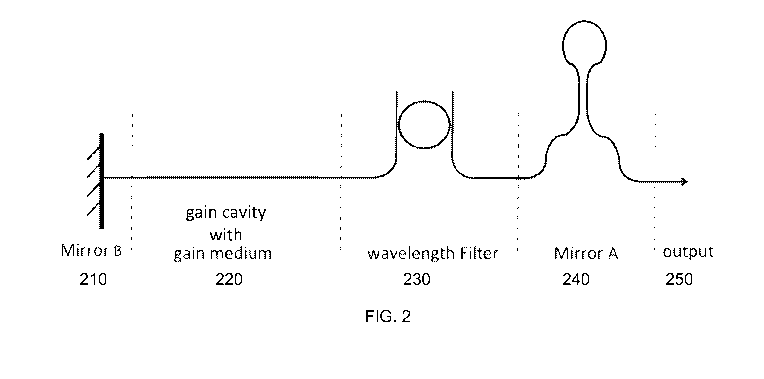
[0035] FIG. 2 is a schematic diagram of a Sagnac loop mirror based laser
cavity
configuration according to principles of the invention.
[0036] FIG. 3A is a graph of the Sagnac loop mirror transmission spectrum
measured
using a tunable laser and grating couplers.
[0037] FIG. 3B is a graph of the transmittance and reflectivity of the
Sagnac loop
mirror as a function of DC coupling length at 1550 nm wavelength.
[0038] FIG. 3C is a graph of the normalized transmittance spectrum.
[0039] FIG. 4 is a graph of a ring filter drop (solid) and through (dashed)
spectrum, and
SOA gain spectrum at 150 mA. The expected lasing wavelength (1552.3 nm) is
indicated by a
star.
[0040] FIG. SA is an image of the testing setup.
[0041] FIG. 5B is a close-up view of the SOA silicon chip interface.
[0042] FIG. SC is a graph of the laser spectrum measured using a fiber
array shows
clear fingerprints of the ring filter and 40 dB SMSR.
[0043] FIG. 6 is a graph of the heterodyne spectrum data (dots) and a
Lorentzian fit
curve with 13.27 MHz FWHM.
[0044] FIG. 7A is a graph showing the spectrum of the AMR drop (solid) and
through
(dashed) ports.
[0045] FIG. 7B is a contour plot for resonant wavelength distribution
across an 8-inch
wafer.
[0046] FIG. 7C is a bar chart of the statistics of the resonant wavelength
distribution.
6
CA 02931399 2016-05-20
WO 2015/077472
PCT/US2014/066657
[0047] FIG. 7D is a schematic of the AMR layout. In one embodiment, wl =
0.3 um,
w2 = 0.46 um, w3 = 0.76 um, and w4 = 0.2 um.
[0048] FIG. 8 is a graph that shows the AMR resonance increase as ring
radius
increases, measured on 31 reticles across an 8-inch wafer.
[0049] FIG. 9 is a schematic diagram of a silicon waveguide to silicon
nitride
waveguide coupler.
[0050] FIG. 10 is a schematic diagram illustrating the mode profile of a
silicon nitride
waveguide of size 4.25 um x 0.2 um.
[0051] FIG. 11A is a graph of the optical spectrum as a function
ofwavelength with 0.1
nm resolution.
[0052] FIG. 11B is a graph of the heterodyne spectrum (dots) as a function
of
frequency offset and a Lorentzian fit curve with 1.28 MHz FWHM.
[0053] FIG. 12A is a graph of laser bias voltage and output power as a
function of
pump current.
[0054] FIG. 12B is a graph of the optical spectrum of the QD 0-Band laser.
[0055] FIG. 13 is a screenshot of eye diagrams of laser output externally
modulated at
Gb/s.
[0056] FIG. 14A is a screenshot of eye diagrams at 40 Gb/s observed in a
control
experiment using a commercial DFB laser.
[0057] FIG. 14B is a screenshot of eye diagrams at 40 Gb/s observed using
the hybrid
silicon external cavity laser according to principles of theinvention.
DETAILED DESCRIPTION
ACRONYMS
[0058] A list of acronyms and their usual meanings in the present document
(unless
otherwise explicitly stated to denote a different thing) are presented below.
AMR Adabatic Micro-Ring
APD Avalanche Photodetector
ARM Anti-Reflection Microstructure
7
CA 02931399 2016-05-20
WO 2015/077472
PCT/US2014/066657
ASE Amplified Spontaneous Emission
BER Bit Error Rate
BOX Buried Oxide
CMOS Complementary Metal-Oxide-Semiconductor
CMP Chemical-Mechanical Planarization
DBR Distributed Bragg Reflector
DC (optics) Directional Coupler
DC (electronics) Direct Current
DCA Digital Communication Analyzer
DRC Design Rule Checking
DUT Device Under Test
ECL External Cavity Laser
FDTD Finite Difference Time Domain
FOM Figure of Merit
FSR Free Spectral Range
FWHM Full Width at Half Maximum
GaAs Gallium Arsenide
InP Indium Phosphide
LiNO3 Lithium Niobate
LIV Light intensity(L)-Current(I)-Voltage(V)
MFD Mode Field Diameter
MPW Multi Project Wafer
NRZ Non-Return to Zero
8
CA 02931399 2016-05-20
WO 2015/077472
PCT/US2014/066657
PIC Photonic Integrated Circuits
PSO Particle Swarm Optimization
ExIff.gy Storai . Emmy Sti3Wil
Q 2-zz x .............. 2, ¨ ....... j; :===
Q Quality factor Emrgy dissi.NAffi pet cycte Nwer Loss
QD Quantum Dot
RSOA Reflective Semiconductor Optical Amplifier
SOI Silicon on Insulator
SEM Scanning Electron Microscope
SMSR Single-Mode Suppression Ratio
TEC Thermal Electric Cooler
WDM Wavelength Division Multiplexing
HYBRID LASER INTEGRATION
[0059] A high quality laser is critical to the performance of any optical
data links.
Because silicon doesn't lase at optical wavelengths used for
telecommunication, external gain
material has to be integrated in a CMOS compatible manner. Silicon waveguide
distributed
Bragg gratings require sub-50 nm feature size and are difficult to
manufacture. A reliable
cavity is also needed to provide feedback for lasing operation. We describe a
novel laser
cavity configuration utilizing a Sagnac loop mirror and micro-ring resonator.
Hybrid lasers
based on such cavity are demonstrated with 1.2 MHz linewidth, 4.8 mW on-chip
output power,
and over 40 dB side mode suppression ratio.
HIGH INDEX CONTRAST SILICON WAVEGUIDES
[0060] FIG. lA is a cross sectional SEM image of submicron silicon
waveguides. Both
the silicon device layer and the buried oxide are clearly visible in FIG. 1A.
The silicon dioxide
layer 110 is 1.7 p.m thick, the silicon waveguide 120 is 0.17 p.m (170 nm)
thick and 0.507 pm
(507 nm) wide, and a lateral repeat distance between silicon structures is
2.774 p.m. The
9
CA 02931399 2016-05-20
WO 2015/077472
PCT/US2014/066657
waveguides are patterned using JBX-6300FS electron beam lithography system and
etched
using an inductively coupled plasma reactive ion etcher.
[0061] FIG. 1B is a perspective view SEM image of submicron silicon
waveguides.
SAGNAC LOOP AND MICRO-RING EXTERNAL CAVITY LASER
[0062] The device was fabricated by a foundry. The Sagnac loop mirror
transmittance
and reflectivity can be predicted analytically as it contains only a
directional coupler other than
a routing waveguide.
[0063] FIG. 2 is a schematic diagram of a Sagnac loop mirror based laser
cavity
configuration of an embodiment of the invention. The Sagnac loop mirror based
laser cavity is
a preferred embodiment. The Sagnac loop Mirror A 240 is made up of a
directional coupler
(DC) with its branches tied together on one side. It contains no ultra-fine
features other than
two parallel waveguides, and can be fabricated by a single etch step.
[0064] In FIG. 2 the filter 230 is a micro-ring that is fixed at a critical
coupling
condition for wavelength filtering, and the Sagnac loop Mirror A 240 is used
for broadband
reflection at one end of the cavity. There is only one output port 250. In
some embodiments,
port 250 can also be used as an input port. The reflectivity of Sagnac loop
Mirror A 240 can be
accurate controlled by adjusting a coupling length. In some embodiments, a
Mirror B 210
having a high reflectivity and low transmittance is used at the other end of
the cavity.
Implementation of Mirror B 210 depends on the gain medium integration
technique. It could
be either the high reflection end of a reflective SOA in the case of edge-
coupled integration or
another Sagnac loop mirror in the case of the direct bonding approach.
[0065] A gain medium is provided in a gain cavity 220. As shown in the
embodiment
of FIG. 2, the Mirror B 210 and the Sagnac loop Mirror A 240 form the ends of
an optical
cavity (or optical resonator) structure. The gain medium in the gain cavity
220 and the filter
230 are provided within the optical cavity structure in serial communication.
In different
embodiments, the gain medium in the gain cavity 220 and the filter 230 can be
provided in any
order, as long as the serial communication is preserved. In preferred
embodiments, for
purposes of convenience of manufacture, it may be helpful to have the filter
230 and the
Sagnac loop Mirror A 240 in physical proximity to each other if the filter 230
is a micro-ring
CA 02931399 2016-05-20
WO 2015/077472
PCT/US2014/066657
filter. In the embodiment illustrated in FIG. 2, the micro-ring filter 230 and
the Sagnac loop
Mirror A 240 are independent and can be optimized separately. This is a robust
device, with
low excess loss.
[0066] In the embodiment illustrated in FIG. 2, a racetrack ring resonator
230 was used
as the wavelength filter. The ring has a radius of 10 lam, and a 1.5 lam long
straight DC to
maintain critical coupling. The ring FSR is 8.7 nm, and FWHM is 0.075 nm,
corresponding to
a Q of 20 000. Because the ring resonator is a comb filter and has multiple
pass bands, the
device is expected to lase at a resonant wavelength near the top of the SOA
gain spectrum.
[0067] In some embodiments, the specific structure of the optical cavity
can include a
reflector that is situated on a silicon chip for example fabricated from an
SOT wafer and the
gain region is provided by a IIIN semiconductor material. The coupling can
include one or
more of butt-coupling, using tapers or inverse tapers for expanded beam
coupling, using lenses
for coupling or lens arrays for coupling.
[0068] In some embodiments, the optical cavity can be operated using
uncooled
operation, in which the temperature is allowed to be free-running. In some
embodiments, the
optical cavity can be operated nonhermetically. In some embodiments, one or
more
components of the optical cavity can be hermetically sealed at the die level.
[0069] In some embodiments, there are included one or more optical coatings
on an
optical facet, either on the silicon side or on the IIIN side or both.
[0070] In various embodiments, the optical cavity provides an optical
output beam that
can comprise a single wavelength of interest, or a plurality of wavelengths of
interest. In some
embodiments the optical cavity provides an optical output beam that is a
narrow linewidth
optical output beam
LASER PHYSICS
100711 An optical cavity or optical resonator comprises mirrors that form a
standing
wave cavity resonator for light waves. Optical cavities are a major component
of lasers,
surrounding the gain medium and providing feedback of the laser light They are
also used in
optical parametric oscillators and some interferometers. Light confined in the
cavity reflects
(or passes) multiple times between the mirrors, producing standing waves for
certain resonance
frequencies. The standing wave patterns produced are referred to as modes.
Longitudinal
11
CA 02931399 2016-05-20
WO 2015/077472
PCT/US2014/066657
modes differ only in frequency while transverse modes differ for different
frequencies and
have different intensity patterns across the cross section of the beam.
[0072] In a laser, there is a gain medium which amplifies light Laser
pumping
involves energy transfer from an external source into the gain medium of a
laser. Different
gain media can be pumped by various methods, which can include the provision
of energy
from electrical sources, optical sources, or even chemical sources. The gain
medium absorbs
energy and creates excited atomic states. When the number of particles in one
excited state
exceeds the number of particles in the ground state or a less-excited state,
population inversion
is achieved. When the excited atomic states relax (return to the ground state)
a photon is
emitted. In lasers, the emission from the excited states can be caused to
happen by the
presence of photons having energy that matches the energy difference between
the excited state
and the ground state. The emitted photons have the same wavelength and
direction and are in
phase with the light that stimulates the excited state to emit, which
condition is termed
coherency. The emission process in lasers is termed stimulated emission, which
is the reason
why the name LASER (Light Amplification by Stimulated Emission of Radiation)
was
selected. In order for laser operation to occur, the pump power must be higher
than the lasing
threshold of the laser.
[0073] In operation, light passes back and forth in the optical cavity
between Mirror A
240 and Mirror B 210. The gain medium in the gaiun cavity 220 amplifies the
light so that the
intensty increases each time the light passes through the gain medium. The
filter 230 filters out
the wavelengths that are not of interest, so that stimulated emissionof those
wavelengths is
suppressed. To the extent that the filter 230 can be used to select one or
nore discrete
wavelengths to pass, the wavelength of the laser light can be tuned.
[0074] Depending on the type of gain medium that is employed, the power to
pump the
gain medium can be selected from any convenient power source having the proper
characteristics (e.g., electrical power, optical power, or the like). In
various embodiments of
the invention, the gain medium can be an electrically pumped gain medium, an
optically
pumped gain medium, or even a chemically pumped gain medium. The gain medium
can be a
solid, a liquid, or a gas.
[0075] FIG. 4 shows a ring filter drop (solid) and through (dashed)
spectrum, and SOA
gain spectrum at 150 mA. The expected lasing wavelength (1552.3 nm) is
indicated by a star.
12
CA 02931399 2016-05-20
WO 2015/077472
PCT/US2014/066657
[0076] From the diagram in FIG. 2, it is straightforward to see that the
Sagnac loop
Mirror A 240 has 100% transmittance for a DC coupling ratio of either 0 or
100%. Since the
DC is symmetric, transmittance T at an arbitrary coupling length, x, can be
predicted by
TC
T = cos2(¨ X + q))
where L is the 100% coupling length, and yo represents the contribution of
coupling from
waveguide bends. Reflectivity equals to 1-T since excess loss of DC is
negligible. To
characterize the Sagnac loop mirror transmittance or reflectivity, structures
shown as Mirror A
240 in FIG. 2 with different coupling lengths, directly connected to two
grating couplers, were
measured using a tunable laser.
[0077] FIG. 3A is a graph of the Sagnac loop mirror transmission spectrum
measured
using a tunable laser and grating couplers. The parabolic line shape and
ripples are caused by
the spectral response of the grating couplers. Reduction in power indicates
decrease of
transmittance as coupling length varies from 3 i.tm to 12 i.tm.
[0078] FIG. 3B is a graph of the transmittance and reflectivity of the
Sagnac loop
mirror as a function of DC coupling length at 1550 nm wavelength. The measured
data
matches well with theory, as is seen in FIG. 3B. The mirror transmittance and
reflectivity can
be accurately controlled by choosing the corresponding coupling length.
[0079] FIG. 3C is a graph of the normalized transmittance spectrum.
Waveguide
confinement decreases as the working wavelength is red shifted, hence
evanescent coupling,
and as a result the reflectivity of the Sagnac loop mirror, is stronger at
longer wavelength, as
shown in FIG. 3C.
[0080] The diced silicon chip was first polished to create a flat and
smooth sidewall for
edge coupling. An ultra-thin edge coupler was employed to match the SOA mode
for low
coupling loss, using the methods described in S. Yang, Y. Zhang, D. W. Grund,
G. A. Ejzak,
Y. Liu, A. Novack, D. Prather, A. E-J Lim, G-Q Lo, T. Baehr-Jones, and M.
Hochberg, "A
single adiabatic microring-based laser in 220 nm silicon-on-insulator," Opt.
Express 22(1),
1172-1180(2013). A half-cavity on silicon chip was aligned to the SOA using a
six-axis stage.
[0081] An image of the testing setup is shown in FIG. 5A. As illustrated in
FIG. 5A, a
cathode probe 510 and an anode probe 560 are used to provide pump current to a
SOA 520.
13
CA 02931399 2016-05-20
WO 2015/077472
PCT/US2014/066657
The SOA was kept at 25 C by a TEC. The silicon chip 530 sat on a metal chuck
and stayed at
room temperature, 15 to 20 C. A lensed fiber 550 was used to collect light
from the high
reflection end of the SOA to monitor the intra-cavity power as a feedback
signal during
alignment. A fiber optic bundle 540 was aligned to probe the output grating
coupler.
[0082] On the silicon chip, the output grating coupler is first connected
to a y-junction,
which has 3 dB intrinsic loss due to power splitting and 0.3 dB excess loss.
One branch of the
y-junction is connected to another grating coupler 127 [tm away, matching the
fiber pitch in the
fiber array, while the other branch lead to the output waveguide of the hybrid
laser. With the
hybrid laser turned off, the fiber array was actively aligned to the grating
coupler loop using an
Agilent laser and power meter. The grating coupler loss was simultaneously
characterized to
be 8.5 dB, which is higher than is typically seen during wafer scale testing,
because it was kept
further to the chip surface as precaution. Then the Agilent laser was turned
off and hybrid
laser turned on, a sharp threshold behavior near 60 mA was observed when
varying the pump
current.
[0083] FIG. 5B is a close-up view of the SOA silicon chip interface.
[0084] The measured spectrum at 170 mA pump current using an optical
spectrum
analyzer with 0.1 nm resolution is plotted in FIG. 5C. Fingerprints of the
ring filter spectral
response are clearly seen in the laser spectrum, with mode spacing equal to
the ring FSR. The
lasing peak appeared at 1552.3 nm, as expected from FIG. 4. The SMSR was 40
dB. On-chip
power was 1.05 mW after normalizing the grating coupler insertion loss. The
major
contributors of cavity loss were the mirror transmittance, 90% at the Sagnac
loop on silicon
chip and 10% at the SOA far-end facet, as well as the coupling loss, estimated
to be over 4 dB.
Angled waveguides were used on both silicon chip and SOA to avoid reflection
into the cavity
at the chip interface.
[0085] We performed heterodyne experiments to measure the laser linewidth.
Our
laser output from the fiber array was combined with the output of a narrow
linewidth laser
(Agilent 81600B, linewidth about 100 kHz) by a 2x2 fiber coupler. The combined
optical
signal (or combined optical beams) was converted into an electrical domain
signal by a
photodetector, whose photocurrent was fed into an RF spectrum analyzer. The
heterodyne
spectrum data is plotted in FIG. 6, together with a Lorentzian fit. The fitted
curve shows that
the FWHM of our laser is approximately 13.17 MHz.
14
CA 02931399 2016-05-20
WO 2015/077472
PCT/US2014/066657
LITHOGRAPHIC MICRO-RING RESONANT WAVELENGTH CONTROL
[0086] As shown in FIG. 5C, although with a high SMSR of 40 dB, a number of
longitudinal modes are available, up to 10 dB over the ASE noise floor. This
is because the
micro-ring is a comb filter, and the SOA gain spectrum is relatively wide and
flat. The laser is
vulnerable to perturbations and the lasing wavelength may hop to the next
cavity longitudinal
mode. It can be addressed by increasing the ring free spectral range (FSR). If
the FSR is wider
than the flat gain spectrum, all other cavity modes will be suppressed.
[0087] A potential drawback of micro-rings is their sensitivity to
fabrication variations.
For wafers processed in a commercial CMOS fab, it has been reported that the
cross-wafer
spread in resonant wavelength is as large as its FSR. If the micro-ring is
used as a WDM
modulator, the ring resonance can be thermally tuned to the nearest grid
channel, thus
mitigating the fabrication sensitivity to a certain extent. However, if the
micro-ring is used
inside a laser cavity, the non-predictability of lasing wavelength may impede
the practical
application of such a device.
[0088] The effect of waveguide geometry variation on micro-ring resonance
wavelength can be modeled as a perturbation to the waveguide effective index.
The FSR
depends on the group index of the waveguide, which is immune to fabrication
errors and can
be accurately controlled among wafers and process lots. If the FSR is
increased to be
significantly larger than the random spread of wavelengths, that spread
determines the range of
possible lasing wavelengths. The spread depends on ring waveguide design, the
SOI wafer,
and silicon processing. We chose an adiabatically widened micro-ring (AMR),
which has a
large FSR and is more robust against fabrication variations. In an AMR, the
waveguide is
narrow near the coupling region to ensure single mode operation, and then is
gradually
widened to support tight bend geometries and a possible need to form a metal
contact. For an
AMR of 2 p.m radius, the FSR is as large as 54 nm.
[0089] FIG. 7A is a graph showing the spectrum of the AMR drop (solid) and
through
(dashed) ports.
[0090] As shown in FIG. 7A, there is only one resonance peak in our testing
laser's
sweepable range, of 1500 nm to 1580 nm. The resonance FWHM is 1.38 nm,
corresponding to
a finesse of 39 or a Q-factor of 1100. We measured the same device design on
all 31 complete
CA 02931399 2016-05-20
WO 2015/077472
PCT/US2014/066657
2.5 cm x 3.2 cm reticles across an 8-inch wafer. The wafer chuck temperature
was set to 30
C, where it is most stable.
[0091] FIG. 7B is a contour plot for resonant wavelength distribution
across an 8-inch
wafer.
[0092] FIG. 7C is a bar chart of the statistics of the resonant wavelength
distribution.
[0093] The resonant wavelength distribution contours are shown in FIG. 7 B
and FIG.
7C and the statistics are listed in Table 1. The mean is 1528.76 nm and the
standard deviation
is 3.32 nm.
[0094] FIG. 7D is a schematic of the AMR layout. In one embodiment, wl =
0.3 lam,
w2 = 0.46 lam, w3 = 0.76 lam, and w4 = 0.2 lam.
[0095] To further validate the predictability of resonant wavelength, AMRs
with
slightly different radii on the same wafer were also measured, and the results
are summarized
in FIG. 8 and Table 2. The wavelength range, maximum minus minimum, falls
between 12.30
nm and 16.30 nm. The standard deviation is between 3.32 nm and 3.78 nm, with
an average of
3.6 nm. The device was patterned using 248 nm lithography on SOI wafers with
20 nm
thickness variations. Significant device uniformity improvement was observed
by switching to
193 nm, 193 nm immersion lithography, and more uniform wafers. For WDM
applications,
the target wavelength can be set as the lower bound of the wavelength spread,
and then locally
and thermally tuned to the grid wavelength and stabilized with active feedback
control. Since
the tuning range is a very small fraction of the FSR, thermal tuning power is
minimal.
Si3N4 EDGE COUPLER
[0096] In some embodiments, one may need to address the low output power
because
of the coupling loss at the chip interface as a result of mode mismatch
between the silicon
waveguide and the RSOA waveguide. The cross-section of a typical silicon
waveguide is
shown in FIG. lA and its mode profile is shown FIG. 10. The near field mode
profile of the
RSOA waveguide is not precisely known, but typical single mode lasers have
mode field
diameters (MFD) around 3 lam x 1 lam. To better match the RSOA mode and reduce
coupling
loss, one can utilize a silicon nitride waveguide edge coupler. Silicon
nitride is a CMOS
compatible material, and commonly used as a hard-mask, in backend of the line
(BEOL)
16
CA 02931399 2016-05-20
WO 2015/077472
PCT/US2014/066657
dielectrics, and as a wafer passivation layer. After the silicon waveguide is
defined, 350 nm of
oxide is deposited and then planarized to 100 nm above silicon waveguide top
surface using
chemical mechanical planarization (CMP). Thereafter 200 nm silicon nitride is
deposited and
patterned by lithography and dry etching.
[0097] FIG. 9 is a schematic diagram of a silicon waveguide to silicon
nitride
waveguide coupler, in which 910 denotes silicon and 920 denotes silicon
nitride.
17
CA 02931399 2016-05-20
WO 2015/077472
PCT/US2014/066657
Table 1
Quartiles
100% Maximum 1535.42
750/ 3rd Quartile 1531.63
50% Median 1528.36
25% 14 Quartile 1526.09
0% Minimum 5122.57
Summary Statistics
Mean 1528.7597
Standard Deviation 3.3156392
Standard Mean Error 0.5955064
31
Table 2
AR (nm) 0 15 25 35 45 55 65
Min 1522.57 1529.71 1533.52 1538.47 1543.00 1552.70 1556.80
Max 1535.42 1542.8 1548.42 1553,70 1559,30 1565.00 1570,41
Range 12.85 13.09 14.90 15.23 16.30 12.30 13.61
Std Dev. 3.32 3.38 3.59 3.75 3.78 3.47 3.62
Table 3
Band Description Wavelength range
0 Original 1260-1360 urn
Extended 1360-1460 nm
short wavelengths 1460-1530 nm
C conventional ("erbium
window") 1530-1565 nm
long wavelengths 1565-1625 nm
ultralong wavelengths 1625-1675 nm
18
CA 02931399 2016-05-20
WO 2015/077472
PCT/US2014/066657
[0098] Light is coupled from silicon waveguide to nitride waveguide using a
push-pull
coupler, as shown in FIG. 9. The silicon waveguide guide width is tapered down
from 0.5 p.m
to 0.18 p.m, while the silicon nitride waveguide width increases gradually
from 0.25 p.m to 1.0
p.m. The insertion loss of this coupler is measured to be 0.3 dB. Then the
silicon nitride
waveguide width is adiabatically tapered to 4.25 p.m. FIG. 10 is a schematic
diagram
illustrating the mode profile of a silicon nitride waveguide of size 4.25 p.m
x 0.2 p.m. The
refractive index of silicon nitride is 1.95 ¨ 2Ø With a 0.2 p.m thickness,
it is guiding, but the
confinement factor is low. In the vertical direction, a large portion of the
mode is in the oxide
cladding, as shown in FIG. 10. The MFD of this silicon nitride waveguide is
3.5 p.m x 0.7 p.m,
better matching a typical SOA mode.
[0099] The alignment and measurement procedure previously described were
repeated
with the ARM and improved edge coupler. After the SOT chip, the RSOA chip and
the fiber
array were properly aligned and the RSOA pump current was turned on. A sharp
threshold
behavior near 60 mA was observed when increasing the pump current. At 170 mA,
about 3
times the threshold current, optical power measured from the power meter is -5
dBm, which
corresponds to on-chip power of 6.8 dBm or 4.8 mW after normalizing the 8.5 dB
grating
coupler insertion loss and 3.3 dB Y-junction insertion loss. The optical
spectrum is plotted in
FIG. 11A and the heterodyne spectrum is plotted in FIG. 11B. The Lorentzian
fit of the
heterodyne spectrum has a full width half maximum (FWHM) of 1.28 MHz,
indicating the
hybrid laser linewidth is about 1.2 MHz.
QD 0-BAND LASER
[00100] One major application of silicon photonics is high-speed data
communications,
such as optical interconnect in data centers. Short reach systems have
standardized in the 0-
Band, the lowest dispersion wavelength window of standard single mode fibers.
Table 3 lists
the wavelength ranges of selected bands that are used in optical communication
systems. Thus
0-Band silicon photonics devices are of great interest. However, almost all
devices
demonstrated up to date operate at C-Band, the fiber low loss window, because
of the wider
availability of lasers, amplifiers, and other testing apparatus at this
wavelength range.
[00101] To first order, passive device geometry scales with wavelength,
free carrier
plasma effect used for modulation is not wavelength sensitive, and germanium
in
19
CA 02931399 2016-05-20
WO 2015/077472
PCT/US2014/066657
photodetectors has stronger absorption at 0-Band. The gain spectrum of typical
materials
cannot cover both wavelengths, so a different gain medium needs to be
considered.
Conventional quantum well lasers can be used, but QD lasers have better
performance in terms
of low threshold current and low thermal sensitivity.
[00102] A QD based RSOA was employed. It is based on indium arsenide
quantum dots
in gallium arsenide with aluminum gallium arsenide barriers and commercially
available off-
the-shelf, for example from Innolume GmbH, Konrad-Adenauer-Allee 11, 44263
Dortmund,
Germany. Facet reflectivity is >99% for the high reflective end and <1% for
the anti-reflective
end. The silicon chip layout and alignment procedure is similar to the
previous device. It
inherits the unique advantages of QD lasers, and maintains the maturity of a
commercial
RSOA, and the CMOS compatibility of the silicon photonics chip.
[00103] FIG. 12A is a graph of laser bias voltage and output power as a
function of
pump current.
[00104] FIG. 12B is a graph of the optical spectrum of the QD 0-Band laser.
[00105] The threshold is at 90 mA. Some kinks due to mode hopping when
current is
swept are also available, which is common to hybrid silicon photonics lasers.
The kink near
250 mA is irregular and most likely due to mechanically or thermally induced
alignment
perturbations. Lasing peak appears at 1302 nm and over 50 dB SMSR is obtained.
[00106] Data transmission experiments were performed to further verify the
viability of
the hybrid external cavity laser. The laser output is non-return to zero (NRZ)
modulated using
a Lithium Niobate (LiNO3) Mach-Zehnder modulator, and detected using an InGaAs
photodetector. The photocurrent is amplified and displayed on a digital
communication
analyzer (DCA). FIG. 13 is a screenshot of eye diagrams of laser output
externally modulated
at 10 Gb/s. A clearly open eye diagram is observed at 10 Gb/s, as shown in
FIG. 13, which is
an overall testament of the laser quality, including linewidth, relative
intensity noise, stability
and other parameters.
[00107] The data rate was then increased to 40 Gb/s. A commercial DFB laser
(Agere
Systems A1611A/B) was used as a control. Longer rise and fall time is observed
because of
system bandwidth limitation. FIG. 14A is a screenshot of eye diagrams at 40
Gb/s observed in
a control experiment using a commercial DFB laser.
CA 02931399 2016-05-20
WO 2015/077472
PCT/US2014/066657
[00108] The same tests were repeated using the hybrid silicon external
cavity laser. FIG.
14B is a screenshot of eye diagrams at 40 Gb/s observed using the hybrid
silicon external
cavity laser according to principles of theinvention. The same level of eye-
openness was
observed, which confirms the device under test is viable for use in high speed
data application
systems.
DESIGN AND FABRICATION
[00109] Methods of designing and fabricating devices having elements
similar to those
described herein are described in one or more of US. Patent Nos. 7,200,308,
7,339,724,
7,424,192, 7,480,434, 7,643,714, 7,760,970, 7,894,696, 8,031,985, 8,067,724,
8,098,965,
8,203,115, 8,237,102, 8,258,476, 8,270,778, 8,280,211, 8,311,374, 8,340,486,
8,380,016,
8,390,922, 8,798,406, and 8,818,141, each of which documents is hereby
incorporated by
reference herein in its entirety.
DEFINITIONS
[00110] As used herein, the term "optical communication channel" is
intended to denote
a single optical channel, such as light that can carry information using a
specific carrier
wavelength in a wavelength division multiplexed (WDM) system.
[00111] As used herein, the term "optical carrier" is intended to denote a
medium or a
structure through which any number of optical signals including WDM signals
can propagate,
which by way of example can include gases such as air, a void such as a vacuum
or
extraterrestrial space, and structures such as optical fibers and optical
waveguides.
[00112] As used herein, the term "optical signal" is intended to denote an
optical wave
or an optical beam having at least one wavelength. Unless otherwise
restricted, the term
"optical signal" can mean, when read in context, any of a broadband signal
spanning a range of
wavelengths, an optical signal having a very narrow wavelength range, or an
optical signal
such as a laser signal having substantially a single wavelength.
[00113] Recording the results from an operation or data acquisition, such
as for
example, recording results at a particular frequency or wavelength, is
understood to mean and
is defined herein as writing output data in a non-transitory or non-volatile
manner to a storage
element, to a machine-readable storage medium, or to a storage device. Non-
transitory or non-
21
CA 02931399 2016-05-20
WO 2015/077472
PCT/US2014/066657
volatile machine-readable storage media that can be used in the invention
include electronic,
magnetic and/or optical storage media, such as magnetic floppy disks and hard
disks; a DVD
drive, a CD drive that in some embodiments can employ DVD disks, any of CD-ROM
disks
(i.e., read-only optical storage disks), CD-R disks (i.e., write-once, read-
many optical storage
disks), and CD-RW disks (i.e., rewriteable optical storage disks); and
electronic storage media,
such as RAM, ROM, EPROM, Compact Flash cards, PCMCIA cards, or alternatively
SD or
SDIO memory; and the electronic components (e.g., floppy disk drive, DVD
drive, CD/CD-
R/CD-RW drive, or Compact Flash/PCMCIA/SD adapter) that accommodate and read
from
and/or write to the storage media. Unless otherwise explicitly recited, any
reference herein to
"record" or "recording" is understood to refer to a non-transitory or non-
volatile record or a
non-transitory or non-volatile recording.
THEORETICAL DISCUSSION
[00114] Although the theoretical description given herein is thought to be
correct, the
operation of the devices described and claimed herein does not depend upon the
accuracy or
validity of the theoretical description. That is, later theoretical
developments that may explain
the observed results on a basis different from the theory presented herein
will not detract from
the inventions described herein.
INCORPORATION BY REFERENCE
[00115] Any patent, patent application, patent application publication,
journal article,
book, published paper, or other publicly available material identified in the
specification is
hereby incorporated by reference herein in its entirety. Any material, or
portion thereof, that is
said to be incorporated by reference herein, but which conflicts with existing
definitions,
statements, or other disclosure material explicitly set forth herein is only
incorporated to the
extent that no conflict arises between that incorporated material and the
present disclosure
material. In the event of a conflict, the conflict is to be resolved in favor
of the present
disclosure as the preferred disclosure.
[00116] While the present invention has been particularly shown and
described with
reference to the preferred mode as illustrated in the drawing, it will be
understood by one
22
CA 02931399 2016-05-20
WO 2015/077472
PCT/US2014/066657
skilled in the art that various changes in detail may be affected therein
without departing from
the spirit and scope of the invention as defined by the claims.
23